 2025, Vol. 36


b Department of Physics and Electronic Engineering, Jinzhong University, Jinzhong 030606, China;
c College of Internet of Things Engineering, Wuxi Taihu University, Wuxi 214026, China;
d Innovation Laboratory for Sciences and Technologies of Energy Materials of Fujian Province (IKKEM), Xiamen 361102, China
With the advantages of outstanding brightness and contrast, excellent energy efficiency, quick short response, and long lifetime, micro-LED display technology hold great promise in wearable technology, augmented reality (AR), virtual reality (VR) head-mounted displays, and naked-eye 3D projections [1–3]. Though significant achievements have been made in recent years, micro-LED displays still exist many challenges, one of them is the realization of full-color displays with low cost. So far, two strategies are evolving, one is assembling of three-color chips onto the driving kit, and the other is color conversion strategy by using fluorescent materials [4,5]. The former utilize mass transfer technology to integrate arrays of red, green, and blue micro-LED chips onto the display backplane, which suffer from low transfer precision, low yield, and high-cost, etc. [6–8]. In contrast, color conversion scheme through conversion of blue or UV light by using red, green and blue light photoluminescent materials, offer a low-cost strategy [9–11].
Synthesis of high quality of fluorescent materials and development of reliable patterning methodology is two critical issues in color conversion approach. Perovskite nanocrystal (PNC) yield luminance with higher color purity and wider color gamut, compared with Ⅱ-Ⅵ quantum dots, such as CdSe [12–16]. Construction of high-resolution PNC structure arrays with micrometer scale dimensions are essential for color conversion based micro-LED displays. To date, researchers have developed various patterning methodology, such as inkjet printing [17–21], photolithography [22–25], electrophoretic deposition [26], microfluidic techniques [27–29], and micro-contact printing [30,31]. Among these methods, inkjet printing is of invincible advantages of high material utilization efficiency and being operated without auxiliary mask. Based on the diversity in driving force, inkjet printing can be classified into piezoelectric inkjet printing [32,33], aerosol jet printing [34,35], and electrohydrodynamic (EHD) inkjet printing [36]. Traditional EHD inkjet printing operates in the Taylor cone-jet mode and requires an external fluid supply pump, nozzle with diameters larger than 200 µm and large distances between the nozzle and substrate (Fig. S1A in Supporting information), and resulted in microstructures with diameter in tens of micrometers [37]. As a comparison, recently developed super-fine electrohydrodynamic inkjet (SIJ) printing technology operates with electrostatic suction driven ink ejection mechanism (Fig. S1B in Supporting information), which requires nozzles with diameters ranging from 0.5 µm to 20 µm and no external fluid supply pump, is capable of producing structures with diameters down to several hundred nanometers [38]. Therefore, SIJ printing is highly suitable for designing ultra-high-resolution color conversion micro-LED display pixels for applications such as AR and VR.
PNC inks for SIJ printing are categorized into precursor inks [39,40] and PNC colloid inks [41,42]. Precursor inks typically involve the dispersion of precursor molecules within polar solvents. The high polarization exhibited by polar solvents under an electric field often results in larger droplets, consequently yielding a relatively large PNC color conversion layer [43]. In contrast, PNC colloid inks involve dispersing pre-synthesized PNCs in appropriate solvents, which produce smaller droplets and enable the arrayed deposition of PNCs [44]. In the context of SIJ inkjet printing utilizing PNC colloid inks, the selection of solvent concerns not only the dispersion and stability of the PNCs but also the following processes in the SIJ printing, including droplet ejection, droplet wetting on the substrate, and solvent evaporation. However, to date, there has been a lack of systematic studies regarding the impact of solvents on SIJ printing conditions for PNC colloid ink and the morphology of the resultant PNC microstructures.
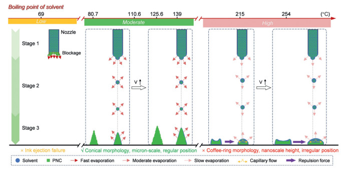
In this work, we selected different solvents to disperse CsPbBr3 PNCs for preparing PNC colloid inks, and systematically studied how the solvent affects the SIJ printing parameters and the resulting PNC microarray structures. Different solvents exhibit a wide range of boiling points, saturated vapor pressures, polarities, dielectric constants, surface tension, and viscosity. Our findings reveal that the boiling point of the solvent is crucial, and selection of non-polar solvent with boiling point within appropriate range is prerequisite for the design of single solvent PNC inks specialized for SIJ printing. Only the boiling point of the solvent falls in the optimal range, the regular positioned, micron-scaled, conical PNC microstructures can be successfully printed (Fig. 1). Below this optimal range, the ink is unable to be ejected from the nozzle; while above this range, irregular positioned microstructures with nanoscale height and coffee-ring-like morphology are produced. The above finding is significantly different from the production of micro/nanostructures using piezoelectric inkjet printing and traditional Tylor-cone mode EHD printing, for which, the ink droplets with relatively large volume were deposited on the substrate, and the surface tension and viscosity play dominant role in the printing process. For SIJ printing of PNC colloid inks, the high surface-to-volume ratio of small ink droplets enhances solvent evaporation, which dominates the formation of the deposited PNC microstructures on the substrate. We hope this work will provide guidelines for design of functional inks for construction of micro/nanostructures by SIJ printing.

|
Download:
|
| Fig. 1. Schematic illustration of the effect of boiling point of solvent on the morphology, size, and locations of the SIJ printed PNC microstructures. | |
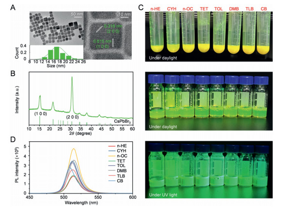
The CsPbBr3 PNCs were synthesized by hot-injection method, and PNCs colloid inks were prepared after PNCs were washed, centrifugated, and dispersed in solvent. After being filtered through 0.22 µm PTFE filter membrane, the PNC colloid inks were printed by SIJ-350 printer. The details of the experimental section are shown in supporting information. To investigate the effect of solvents on the SIJ printed PNC arrays, this study selected aliphatic and aromatic organic solvents with different boiling point, polarity, surface tension and viscosity to disperse the PNCs. Table S1 (Supporting information) shows the parameters of these solvents, and the surface tension and viscosity of the PNC inks dispersed in these solvents are shown in Fig. S2 (Supporting information). The addition of PNCs in the solvent did not induce significant changes in surface tension and viscosity. The CsPbBr3 PNC colloid ink in n-HE were utilized for characterization of PNC. Transmission electron microscope (TEM) image shows the PNCs have cubic shape with narrow size distribution (Fig. 2A). The lattice spacing of PNCs are 0.318 and 0.615 nm correspond to the crystal plane of (200) and (100) of CsPbBr3 PNCs (Fig. 2B), confirming the successful preparation of CsPbBr3 PNCs. After dispersing the same bunch of CsPbBr3 PNCs in different solvents, we conducted TEM and dynamic light scattering (DLS) measurement to study whether the solvent affect the size of PNCs. The cubic shape of PNCs remained intact in n-HE, CYH, n-OC, and DMF, whereas the cubic structure of PNCs was partially disrupted in TET, TOL, TLB, and CB to varying extents (Fig. S3 in Supporting information). DLS measurement results in Fig. S4 (Supporting information) show the average size of CsPbBr3 PNCs in different solvents is ranked as follows: TLB-PNCs > n-OC-PNCs > n-HE-PNCs > TOL-PNCs > DMB-PNCs > CYH-PNCs > TET-PNCs > CB-PNCs. The significantly large average size of the PNCs in TLB measured by DLS may result from the aggregation of apparently collapsed PNCs in TLB (Fig. S3G). Fig. 2C (top) shows the optical images of CsPbBr3 PNCs colloid inks in different solvents with PNC concentration of 225 mg/mL. The PNCs interact differently with solvents of various polarities, which affect their colloidal stability in these solvents. Based on the observation of the precipitates, the stability of CsPbBr3 PNCs in different solvents is ranked as follows: n-HE-PNCs ≈ CYH-PNCs > n-OC-PNCs > TLB-PNCs > TET-PNCs > DMB-PNCs > TOL-PNCs > CB-PNCs. CsPbBr3 PNCs in general exhibit higher colloidal stability in aliphatic solvents compared with aromatic solvents. This is attributed to the long-chain alkane structure of OA and OAm ligands, which reinforces the dispersion of CsPbBr3 PNCs in solvents with similar alkane structures according to the "like dissolves like" principle. By centrifuging the above colloids, collecting the supernatant, and dispersing it in different solvents and filtering with 0.22 µm PTFE membrane, we prepared colloidal inks suitable for SIJ printing. Photographs of these inks under daylight and UV light are shown in Fig. 2C, which shows that all the colloid inks emit bright green light.

|
Download:
|
| Fig. 2. (A) TEM images and size distribution of CsPbBr3 PNCs. (B) XRD characterization of CsPbBr3 PNCs. (C) Photographs of colloid inks with the same concentration of CsPbBr3 PNCs dispersed in different solvents under daylight (top). The centrifuged, re-dispersed, and filtered colloid inks under daylight (middle) and UV light (bottom). (D) PL spectra of the CsPbBr3 PNC colloid inks in different solvents. | |
Fig. 2D shows the PL spectra of PNC colloid inks in different solvents, with PL intensity is ranked as follows: n-OC-PNCs > DMB-PNCs > CYH-PNCs > TOL-PNCs > CB-PNCs > TLB-PNCs > TET-PNCs > n-HE-PNCs. As shown in Fig. 2D and Fig. S5A (Supporting information), PL peak wavelength of PNCs colloid inks in non-polar solvents were about 514 nm, but it exhibited a 6-nm blue shift in polar solvent CB. Increased polarity of the solvent weakens the interaction between the OA/OAm ligands and CsPbBr3 PNCs, leading to ligand detachment and disruption of the octahedral structure [45]. Figs. S5B-D (Supporting information) show the TRPL curves, average fluorescent lifetime and PLQY of PNCs colloid inks in different solvents. PNCs inks achieved the highest PLQY of 56.88% using DMB as the solvent, and PLQY is ranked as follows: DMB-PNCs > TOL-PNCs > n-OC-PNCs > CB-PNCs > CYH-PNCs > n-HE-PNCs > TET-PNCs > TLB-PNCs.
The SIJ printing of PNC colloid inks can be divided into three stages (Fig. 1). At stage 1, PNC ink droplet ejected under electric field. At stage 2, the ejected droplet moves towards the substrate. At stage 3, the ink droplet touches the substrate and forms solid phase structures. Due to the different evaporation rate of the solvents, the colloid inks show different behaviors during the three stages. In the following sections, we will discuss the SIJ printing of PNC inks in different solvents with the order of increasement in boiling point of solvents.
The CsPbBr3 PNCs colloid ink dispersed in n-HE was unable to eject ink droplets from the nozzle even at the largest voltage of 1000 V, the maximum value of the SIJ printer. n-HE has a low boiling point (69 ℃) and a high saturation vapor pressure (147.6 mmHg), resulting in a large evaporation rate. Before being ejected from the nozzle, the solvent molecules of the ink droplet evaporate completely, leading to PNC particle deposition at the nozzle tip and blockage of nozzle, demonstrating the SIJ printing of this ink failed in the first stage. Therefore, highly volatile n-HE is not suitable as a solvent for SIJ printing of CsPbBr3 PNC colloid ink.
When using non-polar solvents (CYH, TOL, n-OC, and DMB) with boiling point ranging from 80.7 ℃ to 139 ℃ for PNC colloid ink preparation, PNC microstructure arrays can be successfully printed by using the corresponding colloid inks. The morphology characterizations show the SIJ printed PNC microstructures feature conical shape and micrometer scale dimension both in diameter and height. In addition, the printed PNCs microstructures were positioned in the pre-designed locations as expected. In the following, we will take SIJ printing of PNC inks in DMB as the representative to show how non-polar solvents with boiling point within this range are appropriate.
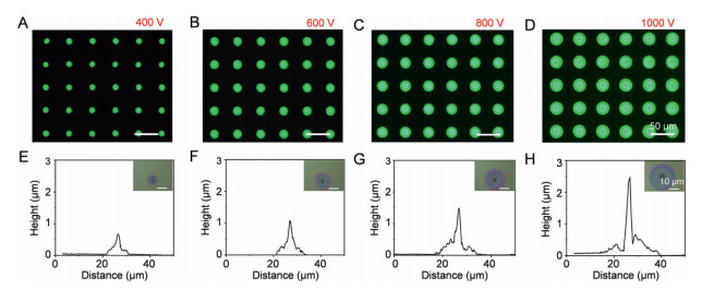
Fig. 3 shows the PNC microstructure arrays and their profile diagrams produced from CsPbBr3 colloid ink dispersed in DMB via SIJ printing under different bias voltages. The printing becomes continuous and stable when the bias voltage exceeds 400 V. Below this threshold voltage, it is failed to eject the PNC inks from the nozzle. Compared with n-HE, DMB has a higher boiling point (139 ℃), which diminishes the solvent evaporation rate and mitigates nozzle clogging, thereby facilitating continuous droplet ejection. The fluorescent images and profile diagrams reveal that the printed PNC microstructure arrays are uniformly distributed and exhibit conical shape. Upon the threshold voltage, the increases in bias voltage enhances the degree of polarization of the ink molecules, intensifying the ink injection per pulse cycle and leading to the increased diameter and height of the arrays. As the printing bias voltage increases from 400 V to 1000 V, the diameter of the microstructures expands from 13.3 µm to 27.1 µm, and the height increases from 0.64 µm to 2.48 µm.

|
Download:
|
| Fig. 3. Fluorescent images (A-D) and profile diagrams (E-H) of PNC microstructure arrays printed with CsPbBr3 colloid ink dispersed in DMB at voltage of 400, 600, 800, and 1000 V, respectively. The microstructure morphology characterized by laser microscopy is shown in the upper right corner of the profile images. | |
Figs. S6-S8 (Supporting information) show the arrays and conical morphologies of CsPbBr3 PNC microstructures printed from the PNC colloid inks in non-polar solvent CYH, TOL, and n-OC with boiling point of 81.7, 110.6, and 125.6 ℃, respectively, under different bias voltages. The threshold voltage for SIJ printing of PNC inks in CYH, TOL, and n-OC is 400, 600, and 1000 V, respectively. The variation trend in the size of the printed PNC microstructures using PNC inks in CYH and TOL under increased voltage over threshold value is similar to that of PNC ink in DMB, and the details are shown in Table S2 (Supporting information).
During the continuous ink ejection, charges are inevitably accumulating in the nozzle tip, thus the droplet are also charged when ejected onto the substrate. As the solvent evaporates, this part of charge drains out via the conducting gold layer on the substrate. If the solvent evaporation does not finish the moment neighboring droplets are ejected, the remnant charges may disturb the electric field at vicinity and cause the irregular positioning of the pixels. Based on the above experimental results, when the boiling point of non-polar solvents falls into the range of 81.7–139 ℃, the micrometer scale PNC microstructures can be printed in the pre-designed locations as expected, suggesting the solvent evaporation speed is appropriate and the accumulated charges of the pre-deposited PNC microstructures did not influence the following deposition processes. In addition, moderate evaporation rate of the droplet on the substrate outcompetes the effect of outward capillary flow, causing rapid deposition of CsPbBr3 PNCs at the center region, which resulted in conical shaped structure. The macro fluorescent images of the PNC microstructure arrays show higher brightness in the central region and decreased brightness towards the edges, which is consistent with the conical morphology of the microstructures.
When using polar solvent CB (boiling point of 132 ℃) for CsPbBr3 PNC colloid ink preparation, the threshold voltage was 800 V, and the diameter of the SIJ printed PNC microstructures increases from 81 µm to 176 µm as the bias voltage increases from 800 V to 1000 V (Fig. S9 in Supporting information). Due to the high relative dielectric constant of 5.61 for CB, the force on CB molecules under the electric field is significantly enhanced, leading to a substantial increase in ink deposition. In contrast, non-polar solvents result in reduced forces under the same electric field and smaller ink volumes. Given the poor stability of CsPbBr3 PNCs in CB and the size requirement for micro-LED display pixels (< 50 µm), polar solvent CB is not suitable for preparing PNC colloid ink for SIJ printing of microstructures for color conversion micro-LED displays.
When the boiling point of non-polar solvent far exceeds 139 ℃, the height of the printed PNC microstructures is significantly reduced, and the morphology changes from conical to coffee-ring like, and the deposited positions deviate significantly from the predetermined position. We think the low evaporation rate of these non-polar solvents is the main factor for these situations.
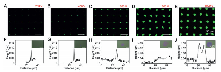
Fig. 4 shows the microstructure arrays and morphologies of CsPbBr3 PNCs printed from colloid ink dispersed in TET (with boiling point of 254 ℃) at different bias voltage. The threshold voltage for printing is 200 V. As the bias voltage increases, the diameter of the printed microstructures also increases. Specifically, when the bias voltage rises from 200 V to 1000 V, the diameter of the structures increases from 2.4 µm to 17.5 µm, but with similiar height of only about 100 nm. The characterizations of the CsPbBr3 PNC microstructure arrays printed from colloid ink dispersed in another non-polar solvent TLB (with boiling point of 215 ℃) are shown in Fig. S10 (Supporting information). At 200 V, the minimum diameters of the printed structures printed from PNC inks in TET and TLB are smaller compared with those printed from CsPbBr3 colloid inks in non-polar solvents such as CYH, TOL, n-OC, and DMB with moderate boiling point, indicating higher printable resolutions by these inks. However, the height of about 100 nm is significantly smaller than the required several micrometer scale thicknesses patterned film, and will lead to limited fluorescence conversion efficiency, luminescence of pixels and significant blue light leakage [46].

|
Download:
|
| Fig. 4. Fluorescent images (A-E) and profile images (F-J) of CsPbBr3 PNC microstructure arrays printed with colloid ink dispersed in TET at bias voltage of 200, 400, 600, 800, and 1000 V, respectively. The microstructure morphology characterized by laser microscopy is shown in the upper right corner of the profile images. | |
The microstructures printed using TET and TLB as the solvent usually exhibited pronounced coffee-ring like morphology. As the bias voltage increases, the volume of ejected ink gradually increases, and the high boiling points of TET and TLB make the deposited droplet maintain its liquid state for a long time. For deposited PNC droplets on the substrate, the solvent evaporation rate at the edges is higher than at the center, which drives the outward capillary flow of CsPbBr3 PNCs, resulting in a coffee-ring like morphology. In addition, due to the low evaporation speed of TET and TLB, the pre-deposited ink droplet cannot become uncharged in a short time, and the accumulated charges in these droplets repel the following charged droplet during the falling and deposition processes, resulting in the unexpected irregular positioned PNC arrays. At lower bias voltages, the diameter of the ink droplets on the substrate is much smaller than the distance between adjacent printing points, thus the repulsion is not sufficiently strong to affect the positioning of neighboring droplets. This deviation in locations becomes significant with the increasement of the ink volume and decrement of adjacent two droplets as the bias voltage increases to 800 V and above.
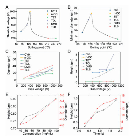
Based on the above studies, we found that the threshold voltage for SIJ printing and minimum diameter of the printed PNC microstructures initially increase and, after reach peaks at boiling point about 120 ℃, both decrease with the increasing solvent’s boiling point (Figs. 5A and B). For PNC colloid ink using the same non-polar solvent, both the diameter and height of the printed microarrays increase with the increasing bias voltage (Figs. 5C and D). To study how the concentration of the PNC influences the SIJ printed PNC microstructures, we prepared PNC ink in DMB with appropriate concentration ranging from 40 mg/mL to 100 mg/mL (Fig. S11 in Supporting information) and found the diameter and height of the printed PNC microstructures increased with the concentration at bias voltage of 600 V (Fig. 5E and Fig. S12 in Supporting information). We also conducted SIJ printing of PNC ink in DMB in different time and found both the diameter and the height of printed PNC microstructures increased with the printing duration (Fig. 5F).

|
Download:
|
| Fig. 5. The relationship between the (A) threshold voltage and (B) minimum diameter of the printed PNC microstructures and the boiling point of the selected non-polar solvent. (C) Diameter and (D) height of SIJ printed PNC microstructures from CsPbBr3 colloid inks dispersed in different solvents at varying bias voltage. The influence of (E) the concentration of PNC dispersed in DMB and (F) the printing duration on the diameter and the height of the SIJ printed PNC microstructures. | |
Comprehensively considering the performance of the PNC colloid ink, relatively low threshold voltage during printing, and the conical shape, micrometer scale and accurate positioning of the printed PNC microstructures, we think DMB is a good choice for dispersing PNCs for constructing PNC CCLs through SIJ printing technology. As a demonstration, we prepared high luminescent PNC CCLs with high printing resolution (1730 dpi), logo of "Xiamen University", and letters "CCL" by CsPbBr3 PNC colloid ink dispersed in DMB (Figs. 6A-C).

|
Download:
|
| Fig. 6. Fluorescent images of (A) high resolution dot arrays, (B) logo of "Xiamen University", and (C) letters "CCL" printed from PNC colloid ink in DMB. | |
The DMB used here is a mixed solvent of o-xylene, m-xylene, and p-xylene. The o-xylene, m-xylene, and p-xylene have similar boiling points, but different values in polarity, surface tension and viscosity. We prepared PNC inks in these three pure solvents, characterized their surface tension and viscosity (Fig. S13A in Supporting information), and printed PNC structures at same bias voltage of 800 V. As shown in Figs. S13B-F (Supporting information), the printed PNC microstructures were conical, with micrometer scale dimensions in both diameter and height. The height/diameter ratio of CsPbBr3 PNCs is ranked as follows: o-xylene-PNC > DMB-PNC > m-xylene-PNC > p-xylene-PNC.
We also prepared mixed solvent of DMB and TLB with different volume ratio to investigate further confirm the effect of the boiling point of non-polar solvent on the SIJ printing effect. As shown in Fig. S14 (Supporting information), even for PNC ink in mixed solvent with volume ratio of DMB: TLB = 1:3, the printed PNC microstructures show coffee-ring like morphology and nanometer scale thickness. For SIJ printing of this mixing solvent ink system, most of the DMB evaporated before the droplets touch the substrate, and deposition behavior of PNC ink in the mixed solvent on the substrate was similar to PNC ink in TLB.
This work focuses on the effects of solvent on the SIJ printing of PNC microstructures for color conversion applications. The boiling point of the non-polar solvent is the dominant factor for SIJ printing of PNC colloid ink, and the selection of non-polar solvent with medium boiling point is prone to obtain PNC microstructure arrays with desired morphology and size. When DMB is used as a solvent, the colloid ink possesses the highest PLQY, and the microstructures can be printed at lower bias voltages. In addition, the uniformly distributed microarrays and the micron-scale diameter and height of the printed microstructures make DMB as the best choice for preparing PNC colloid ink. In the future, solvent engineering should be integrated with ligand engineering and coating techniques of quantum dots to comprehensively enhance both the morphology and luminescent performance of SIJ printed color conversion microstructures.
Declaration of competing interestThe authors declare that they have no known competing financial interests of personal relationships that could have appeared to influence the work reported in this paper.
CRediT authorship contribution statementShuli Wang: Writing – original draft, Investigation, Funding acquisition, Formal analysis, Data curation, Conceptualization. Xuemin Kong: Methodology, Formal analysis. Siting Cai: Writing – original draft, Investigation. Yunshu Luo: Writing – review & editing. Yuxuan Gu: Visualization, Investigation. Xiaotong Fan: Writing – review & editing. Guolong Chen: Methodology. Xiao Yang: Writing – review & editing, Supervision, Methodology, Formal analysis. Zhong Chen: Writing – review & editing. Yue Lin: Writing – review & editing, Supervision, Resources, Project administration, Funding acquisition.
AcknowledgmentsThis work is supported by the National Natural Science Foundation of China (No. 62374142), Fundamental Research Funds for the Central Universities (Nos. 20720220085 and 20720240064), External Cooperation Program of Fujian (No. 2022I0004), Major Science and Technology Project of Xiamen in China (No. 3502Z20191015), Xiamen Natural Science Foundation Youth Project (No. 3502Z202471002).
Supplementary materialsSupplementary material associated with this article can be found, in the online version, at doi:10.1016/j.cclet.2025.110976.
| [1] |
W. Chang, J. Kim, M. Kim, et al., Nature 617 (2023) 287. DOI:10.1038/s41586-023-05889-w |
| [2] |
L.M. Kong, Y.Q. Sun, B. Zhao, et al., Nature 631 (2024) 73-79. DOI:10.1038/s41586-024-07531-9 |
| [3] |
K. Behrman, I. Kymissis, Nat. Electron. 5 (2022) 564-573. DOI:10.1038/s41928-022-00828-5 |
| [4] |
J.E. Ryu, S. Park, Y. Park, et al., Adv. Mater. 35 (2023) 2204947. |
| [5] |
Z. Chen, S.K. Yan, C. Danesh, J. Phys. D: Appl. Phys. 54 (2021) 123001. DOI:10.1088/1361-6463/abcfe4 |
| [6] |
Z.M. Luo, B.X. Liu, T. Zheng, et al., ACS Photonics 9 (2022) 2422-2430. DOI:10.1021/acsphotonics.2c00496 |
| [7] |
D. Peng, K. Zhang, V.S.D. Chao, et al., J. Disp. Technol. 12 (2016) 742-746. |
| [8] |
J.Z. Song, J.H. Li, X.M. Li, et al., Adv. Mater. 27 (2015) 7162. DOI:10.1002/adma.201502567 |
| [9] |
Z. Gong, E. Gu, S.R. Jin, et al., J. Phys. D: Appl. Phys. 41 (2008) 094002. DOI:10.1088/0022-3727/41/9/094002 |
| [10] |
X. Zhang, J.H. Cai, L.W. Yang, et al., ACS Energy Lett. 9 (2024) 1587-1603. DOI:10.1021/acsenergylett.3c02454 |
| [11] |
Y.Y. Wang, R.C. Wang, Y.C. Ge, et al., ACS Appl. Mater. Interfaces 16 (2024) 29132-29140. DOI:10.1021/acsami.4c01936 |
| [12] |
Y.H. Wang, Y.S. Luo, X.M. Kong, et al., Nanoscale 17 (2025) 1764-1789. DOI:10.1039/d4nr03925d |
| [13] |
B. Wang, L. Liu, Y. Zhang, et al., Chin. Chem. Lett. 31 (2020) 295-298. |
| [14] |
H. Lin, S. Zhang, D. Zhao, et al., Chin. Chem. Lett. 36 (2025) 109795. |
| [15] |
X.T. Fan, S.L. Wang, X. Yang, et al., Adv. Mater. 35 (2023) 2300834. |
| [16] |
C. Geng, S. Xu, H.Z. Zhong, et al., Angew. Chem. Int. Ed. 57 (2018) 9650-9654. DOI:10.1002/anie.201802670 |
| [17] |
S.Q. Jia, G.Y. Li, P. Liu, et al., Adv. Funct. Mater. 30 (2020) 1910817. |
| [18] |
W.H. Bai, T.T. Xuan, H.Y. Zhao, et al., Adv. Opt. Mater. 10 (2022) 2200087. |
| [19] |
J.H. Cai, W.Z. Lai, Y. Chen, et al., Laser Photonics Rev. 18 (2024) 2400298. |
| [20] |
X. Yang, S.L. Wang, Y.Q. Hou, et al., Nano Lett. 24 (2024) 3661-3669. DOI:10.1021/acs.nanolett.3c04927 |
| [21] |
C.T. Wei, W.M. Su, J.T. Li, et al., Adv. Mater. 34 (2022) 2107798. |
| [22] |
C.D. Dieleman, J. van der Burgt, N. Thakur, et al., ACS Appl. Energy Mater. 5 (2022) 1672-1680. DOI:10.1021/acsaem.1c03091 |
| [23] |
F. Palazon, Q.A. Akkerman, M. Prato, L. Manna, ACS Nano 10 (2016) 1224-1230. DOI:10.1021/acsnano.5b06536 |
| [24] |
P.P. Zhang, G.L. Yang, F. Li, et al., Nat. Commun. 13 (2022) 6713. |
| [25] |
S. Lu, Z. Fu, F. Li, et al., Angew. Chem. Int. Ed. 61 (2022) e202202633. |
| [26] |
J. Yang, D. Hahm, K. Kim, et al., Nat. Commun. 11 (2020) 1. |
| [27] |
P.Y. Li, J. Tao, Y.Z. Zhao, et al., Micromachines 13 (2022) 448. DOI:10.3390/mi13030448 |
| [28] |
Y. Li, J. Tao, Q. Wang, et al., Appl. Phys. Lett. 118 (2021) 173501. |
| [29] |
L. Zhu, J. Tao, P. Li, et al., Nanoscale Adv. 5 (2023) 2743-2747. DOI:10.1039/d2na00765g |
| [30] |
M.K. Choi, J. Yang, K. Kang, et al., Nat. Commun. 6 (2015) 7149. |
| [31] |
S.V. Makarov, V. Milichko, E.V. Ushakova, et al., ACS Photonics 4 (2017) 728-735. DOI:10.1021/acsphotonics.6b00940 |
| [32] |
F. Zhang, Z.F. Shi, S. Li, et al., ACS Appl. Mater. Inter. 11 (2019) 28013-28022. DOI:10.1021/acsami.9b07518 |
| [33] |
M.A.P. Mahmud, T. Tat, X. Xiao, et al., Exploration 1 (2021) 20210033. |
| [34] |
H.V. Han, H.Y. Lin, C.C. Lin, et al., Opt. Express 23 (2015) 32504-32515. |
| [35] |
N.J. Wilkinson, M.A.A. Smith, R.W. Kay, R.A. Harris, Int. J. Adv. Manuf. Technol. 105 (2019) 4599-4619. DOI:10.1007/s00170-019-03438-2 |
| [36] |
J. Schneider, P. Rohner, D. Thureja, et al., Adv. Funct. Mater. 26 (2016) 833-840. DOI:10.1002/adfm.201503705 |
| [37] |
M.M. Laurila, A. Soltani, M. Mäntysalo, Inkjet printed single layer high-density circuitry for a MEMS device, in: 2015 IEEE 65th Electronic Components and Technology Conference (ECTC), San Diego, U. S. A., May 26-29, 2015, pp. 968–972.
|
| [38] |
Z. Abbas, D.Z. Wang, Z.Y. Du, et al., Microelectron. Eng. 237 (2021) 11496. |
| [39] |
M.H. Zhu, Y.Q. Duan, N. Liu, et al., Adv. Funct. Mater. 29 (2019) 1903294. |
| [40] |
H.G. Li, N. Liu, Z.L. Shao, et al., J. Mater. Chem. C 7 (2019) 14867-14873. DOI:10.1039/c9tc04394b |
| [41] |
S. Yakunin, J. Chaaban, B.M. Benin, et al., Nat. Commun. 12 (2021) 981. |
| [42] |
J.Y. Liu, B. Shabbir, C.J. Wang, et al., Adv. Mater. 31 (2019) 1901644. |
| [43] |
X.T. Fan, X. Yang, X.M. Kong, et al., Next Nanotechnology 5 (2024) 100045. |
| [44] |
X.M. Kong, X.T. Fan, Y.H. Wang, et al., Nano Mater. Sci. 7 (2025) 49-64. |
| [45] |
X.Y. Jin, K.L. Ma, H.F. Gao, J. Am. Chem. Soc. 144 (2022) 20411-20420. DOI:10.1021/jacs.2c08622 |
| [46] |
Y.H. Chen, X. Yang, X.T. Fan, et al., ACS Appl. Mater. Inter. 16 (2024) 24908-24919. DOI:10.1021/acsami.4c02594 |