 2024, Vol. 35


b Shenzhen Key Laboratory of Advanced Thin Films and Applications, Key Laboratory of Optoelectronic Devices and Systems of Ministry of Education and Guangdong Province, College of Physics and Optoelectronic Engineering, Shenzhen University, Shenzhen 518060, China
Solar energy has become the most attractive renewable energy source at present, and the development of highly efficient and low-cost solar cells is essential for the realization of sustainable development. Kesterite Cu2ZnSn(S, Se)4 (CZTSSe) is regarded as an alternative for Cu(In, Ga)Se2 (CIGS) solar cells due to the abundant earth's storage and high power conversion efficiency (PCE) [1–3]. However, the PCE of CZTSSe solar cells (14.9%) is still much lower than that of the best performance of CIGS (23.6%) [1,4]. It is shown that large open-circuit voltage (VOC) deficit and low fill factor (FF) are the main limitations of CZTSSe solar cells, which arise from carrier recombination due to complex and diverse recombination centers in the device [5,6]. Potential recombination centers in the CZTSSe absorber include deep defects, voids, and grain boundary. Further improvement of the VOC and FF to increase the efficiency of CZTSSe devices is an urgent priority [7–9].
As the best thin-film photovoltaic technology for commercial application, CIGS is very worthy of reference for its efficiency enhancement process, and alkali doping is an effective strategy to significantly improve the PCE of CIGS [10–12]. Alkali doping has also been proved to improve the performance of CZTSSe devices. Light alkali metal (Li, Na) doping can increase the carrier concentration of CZTSSe, reduce the point defects, and promote the growth of absorber grain [13–15]. Heavier alkali metal (Rb, Cs) doping can enhance the charge selectivity of the CZTSSe absorber [16,17]. Normally light alkali metals tend to enter the grains and distribute inside the grains, while heavy alkali metals tend to distribute at the grain boundary [11,18]. The alkali elements in the precursor film react with Se in the early stage of selenization to form alkali metal-Se liquid intermediate phase to improve the crystallinity of the absorber and passivate the grain boundary, which is conducive to the enhancement of VOC and FF [19–21]. K atoms combine the advantages of both heavy and light bases due to the medium atomic size, and related studies have shown that K doping can enhance the (112)-optimized orientation of CZTSSe thin films, increase the grain size, and reduce the secondary phases [14]. However, the specific properties of K doping to improve device performance and the key factors to passivate grain boundary are not known, and the mechanism of K doping to improve grain growth needs further investigation.
In this work, we realized K doping by introducing a K2S layer on the absorber surface by simple spin-coating process. We explored the effect of K doping on the grain growth process, electrical and defect properties of CZTSSe thin films. K doping improves the crystallization process, reduces interface and bulk defects, and suppresses carrier recombination. At the same time, we found that carrier separation at the grain boundary of K-doped samples was enhanced, which we inferred to be due to the presence of the wide bandgap compound K2Sn2S5. This work provides a simple and economical method for fabricating highly efficient CZTSSe devices. Meanwhile, the suppression of grain boundary recombination by the wide bandgap compound K2Sn2S5 provides new insights into the enhancement of carrier separation ability.
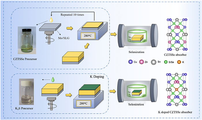
The preparation method of the precursor solution and the assembly process of the CZTSSe device are shown in detail in the previous work [2]. K2S solution was obtained by dissolving K2S powder in ethanol and the concentrations of K2S solution were 0.01, 0.05 and 0.1 mol/L respectively. K doping was realized by spin-coating K2S solution on the surface of the precursor (Fig. 1), and the K content in the absorber was regulated by controlling the concentration of K2S solution. The spin-coating speed was kept at 3000 rmp for 20 s. The temperature of the hot plate was 280 ℃.

|
Download:
|
| Fig. 1. K doping CZTSSe precursor film preparation process diagram and the crystal structure. | |
Figs. S1a–d (Supporting information) show the cross-sectional morphology measured by scanning electron microscopy (SEM) of the absorber with different K contents. The reference sample has a typical double-layer grain structure, with the thickness of the upper large grain and the bottom fine grain being about 600 nm. The thickness of the upper large grain is significantly increased by K doping, and the thickness of the upper large grains increases to 800 nm when the concentration of the K2S solution is 0.01 mol/L. When the concentration of K2S solution was 0.05 mol/L, the thickness of the large grain of the upper layer was 1 µm. Further increasing the concentration of K2S solution, the grain size of the absorber increases accompanied by a large number of voids, which may be attributed to the segregation of K-related compounds in the absorber [10]. Figs. S1e-h (Supporting information) show the efficiency box statistics of the device for samples doped with different K. K doping can significantly improve the device performance, and the optimal device efficiency is 13.04% with K2S solution concentration of 0.05 mol/L. Increasing the K2S concentration to 0.1 mol/L, the significant decrease in VOC was attributed to the creation of a large number of voids in the absorber layer due to excess K. Meanwhile, compared to the samples with 0.01 mol/L K2S, the FF of the devices decreased to a certain extent when the K2S concentration was increased to 0.05 and 0.1 mol/L, which may be caused by the segregation of K-related compounds on absorber surface due to the increase in K2S concentration (marked in red in Figs. S1c and d).
In order to investigate the intrinsic reason for the improvement of the crystallinity of the absorber due to K doping, we performed SEM measurements on the reference and optimal samples (K2S solution concentration of 0.05 mol/L) with different selenization times (0/300/600/900 s), and the results are displayed in Fig. S2 (Supporting information). In the following the reference sample is abbreviated as Reference and the sample with K2S solution concentration of 0.05 mol/L is abbreviated as K doping. The precursor films of the two samples showed similar loose and porous states, and the grains were formed at the surface and back interfaces when the selenization time was 300 s. The grain thicknesses at the surface and back interfaces of the K doping sample were larger than those of the Reference sample. When the selenization time was extended to 600 s, the two samples showed a similar three-layer structure, in which the upper and lower layers had large grains and the middle layer had fine grains (The upper and lower grains are marked in green and yellow, respectively. The middle grains are shown in blue). The thickness of the large grain of the upper and lower layers of the Reference sample is almost equal, while the thickness of the upper grain of the K doping sample is much thicker than that of the lower layer. When the selenization time is further extended to 900 s, the top and bottom grain contact each other then merge and grow, and the fine grain layer in the middle of the film was disappeared. The thickness of the large grains at the top and the fine grains at the bottom of the Reference absorber is about 600 nm, whereas the thickness of the large grains at the top of the K doping absorber is 1 µm. The improvement of the crystallinity of the absorber by K doping is very obvious, which is attributed to the formation of a series of low-melting-point K-Se phases during the selenization process due to the high chemical affinity energy of K and Se [12]:

|
(1) |

|
(2) |

|
(3) |
These liquid K-Se phases can lower the melting point and promote grain growth [22]. At the same time, the presence of K-Se phases can make the grain growth environment more Se-rich, so that selenization can proceed more fully [10,12].
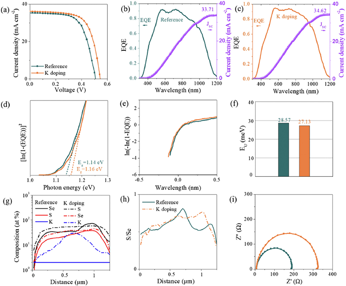
The current density-voltage (JV) curves of the Reference device and the K doping device are shown in Fig. 2a and the results are shown in Table S1 (Supporting information). The series resistance (Rs) and parallel resistance (Rsh) of the Reference and K doping devices are shown in Figs. S3 and S4 (Supporting information). The reference device has a large Rs and a small Rsh. In general, FF is inversely proportional to Rs and directly proportional to Rsh. Therefore, the smaller Rs and larger Rsh of the K doping devices favor FF. The external quantum efficiency (EQE) curves of the two samples and the integral current density calculated from the EQE curves are illustrated in Figs. 2b and c. The EQE intensity of the K doping device in the range of 500–1000 nm is significantly increased, and the higher quantum production rate suggests that K doping contributes to the enhancement of the carrier collection efficiency (Fig. S5 in Supporting information) [23]. The integral current density of the Reference device and the K doping device are in close agreement with the device's short-circuit current density (JSC), which is in agreement with the J-V test results [24,25]. Fig. 2d shows the bandgap values obtained by fitting the EQE band tails, which are slightly larger for the K doping device than for the Reference device. It may be attributed to the additional S introduced by the K2S [26,27]. Fitting the band tails to the EQE curves enables the calculation of the Urbach energy (Eu) [28]. Internal disorder and defect states in the absorber lead to the presence of band-tailed states, and Eu is a key parameter for measuring the scale of the band-tailed states in the absorber [29,30]. The smaller Eu of the K doping device (Figs. 2e and f) implies that both the defect density and the disorder level in the doped film have been suppressed.

|
Download:
|
| Fig. 2. (a) J-V characteristics of reference and K doping device. (b) EQE and the integrated current density of reference device. (c) EQE and the integrated current density of K doping device. (d) Bandgap of reference and K doping device calculated from EQE curves. (e) Eu of reference and K doping device calculated from EQE curves. (f) The calculation result of Eu. (g) S and Se elemental line scans of reference and K doping film. (h) S/Se profiles and bandgap profiles of reference and K doping films. (i) The EIS curves for the reference and K doping devices. | |
The distribution of K in CZTSSe was tested by SEM-EDS (energy dispersive spectroscopy) and the results are shown in Fig. 2g. It can be seen that K successfully diffused into the absorber of the K doping sample. The S and Se profiles of the two samples are quite different, the K doping significantly increases the S and Se content and changes their longitudinal distribution. We used K2S as the K source thus introducing additional S, the absorber of the K doping sample has higher S content, which is the reason for the larger bandgap of the K doping device. K has a higher affinity energy with Se and tends to react with Se to generate a series of K-Se compounds to promote crystallization, and the presence of these K-Se compounds as Se source enables the K doping samples to be more fully selenized [31,32]. The EDS data show that the Se content of the reference film is higher at the bottom, and the Se distribution in the K doping film is more uniform, indicating that the presence of K can optimize the Se distribution in the absorber. The S/Se profiles of the two samples were shown in Fig. 2h. The bandgap profile of the K2S sample showed a smaller variation, which implies that the K doping sample is more homogeneous.
The effect of the K doping process on the charge transfer performance of the device was tested by electrochemistry impedance spectroscopy (EIS) and the results are displayed in Fig. 2i. Fig. S6 (Supporting information) shows the equivalent circuit diagram containing the series resistance (Rs*), the recombination resistance (Rrec), and the chemical capacitance (Crec) [33,34]. The diameter of the semicircle in the EIS curve is equal to the recombination resistance of the device. Typically, a larger series resistance means better transportation performance, and a larger recombination resistance means less electron and hole recombination in the device [35]. It can be seen that the K doping devices have large recombination resistance and small series resistance, which indicates that K doping can effectively reduce the carrier recombination and improve the charge transfer performance of the devices.
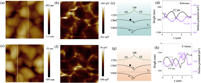
We determined the surface morphology and surface potential of the absorber by atomic force microscope (AFM) and Kelvin electrostatic force microscopy (KPFM). Fig. 3 shows the surface morphology, surface potential, and the variation curves of roughness and potential for the Reference and K doping films. It can be seen that the grain boundary potentials of both films are higher than the grain interior potentials, which is favorable for the formation of hole potential barriers at grain boundary to reduce the grain boundary carrier recombination (Figs. 3c and g show a schematic of the grain boundary and grain interior potentials) [36]. The curves in Figs. 3d and h show that the roughness of the Reference film surface has greater roughness than that of the K doping film, and the larger roughness is detrimental to the p-n junction quality and reduces the FF. The surface contact potential difference (CPD) between grain boundary and grain interior is larger in K doping film (Note 1 in Supporting information) [37,38]. Within a certain range, the larger CPD favors the formation of more effective hole barriers at grain boundary and enhances the carrier separation ability at the grain boundary. During the growth of K-doped CZTSSe films, K tends to generate compound K2Sn2S5 with Sn.

|
(4) |

|
Download:
|
| Fig. 3. AFM and KPFM of the (a, b) reference and (e, f) K doping film. The schematic of the grain boundary and grain interior potentials of (c) reference film and (g) K doping film. The potential variation of (d) reference film and (h) K doping film. | |
Theoretical calculations show very low formation energy (−7.36 eV) of this compound in K-doped CZTSSe films [39]. Since K does not have the 3d orbitals for hybridization with S 3p orbitals, the VBM of this wide band gap alkali metal compound is much smaller. K combines the properties of both light and heavy alkali metals and is able to enter the grain interior to passivate defects as well as to segregate at the grain boundary. We hypothesize that the increase in CPD at grain boundary is due to the formation and accumulation of wide bandgap compound K2Sn2S5, which contributes to the enhancement of the charge transport capability of the absorber.
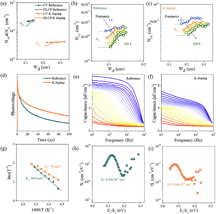
Capacitance-voltage (CV) and drive-level capacitance spectroscopy (DLCP) are one of the powerful tools for analyzing carrier concentration (Nc), depletion region width (Wd), and defect density in thin film solar cells. Fig. 4a shows the CV and DLCP curves for Reference and K doping devices. The DLCP analysis is not sensitive to the interface state, and the intercept with the y-axis at zero bias is the Nc in the absorber, and the intercept with the x-axis is the Wd [40]. The calculation results are shown in Table S2 (Supporting information). The reduced Nc in K-doped devices may be attributed to the reduction of VCu due to the occupation of Cu sites by K. The Wd of K-doped devices is larger than that of Reference devices, which is favorable for the collection and separation of carriers. Compared to DLCP, CV analysis is more sensitive to the interface state, so the difference between the CV data and the DLCP data is the interface defect density (NIT) of the device [41]. K doping reduces the NIT from 6.87 × 1015 cm−3 to 1.03 × 1015 cm−3. The lower interface state density facilitates the obtaining of a better PN junction quality and the reduction of interface recombination. In addition, DLCP measurements performed at high frequency can obtain free carrier responses, while DLCP measurements performed at low frequency can obtain both free carrier and defect responses. Thus the difference between the low and high frequency DLCP data is the bulk defect density (NT) [42]. The NT of the reference device and the K doping device are 8.52 × 10¹⁵ and 1.68 × 1015 cm−3 (Figs. 4b and c), respectively. The lower interface defect density and bulk defect density of the K doping device are attributed to the fact that the K doping device has higher S and Se content, which passivates the VSe and VS defects. Meanwhile, K atoms occupy Cu sites, which can effectively reduce the density of VCu and CuZn defects. What's more, the presence of K can promote the element diffusion and stabilize the Sn content, which is conducive to inhibiting the formation of Sn-related defects [43].

|
Download:
|
| Fig. 4. (a) The plot of CV and DLCP for devices reference and K doping. DLCP measured at frequencies from 1 kHz to 200 kHz for (b) reference and (c) K doping device. (d) TPV spectra of Reference and K doping device. Admittance spectral results for (e) reference device, (f) K doping device, from the inflection points of the AS results. (g) The Arrhenius plots of reference device and K doping device. The defect density of states (Nt) for (h) reference device, (i) K doping device. | |
The transient photovoltage (TPV) spectra is utilized to evaluate the carrier lifetime of solar cells [44]. Fig. 4d shows the TPV curves of the Reference sample and the K doping sample. The fitting results show that the TPV lifetimes (τTPV) of the reference and K doping devices are 20.72 µs and 28.43 µs, respectively. The increased TPV lifetime facilitates the photogenerated carriers to be transported to the electrodes, implying that the non-radiative recombination is suppressed [45,46]. Therefore, K doping reduces the defect concentration in the absorber and decreases the recombination chances of photogenerated carriers, which is conducive to optimizing the carrier transport performance of the device.
To investigate the effect of K doping on the defect properties in more depth, the reference device and the K doping device were examined by admittance spectroscopy (AS). The tests were performed in the temperature range of 300–110 k with a temperature interval of 10 k. The AS curves (Figs. 4e and f), Arrhenius curves (Fig. 4g), and calculated defect density (Figs. 4h and i) are illustrated in Figs. 4e-i (Note 2 in Supporting information). The capacitance of the reference device varies greatly with frequency, and this significant frequency dependence implies that there are more recombination centers in the reference absorber. The defect recombination activation energy is obtained from the inflection point corner frequency fitting of each capacitance frequency curve, and the activation energy of the K doping device (76 meV) is small compared to that of the reference device (109 meV) [47,48]. The lower activation energy is less likely to be an effective recombination center, and the lower degree of recombination in the K doping devices favors the VOC [48–50]. In addition, the defects with activation energy around 100 meV are attributed to CuZn and ionization produces hole carriers, thus the CZTSSe absorber has P-type conductivity. The K doping devices have a lower defect density, consistent with the lower carrier concentration due to K doping in DLCP.
In summary, we doped K in the CZTSSe absorber by a convenient spin-coating process, and the low-melting-point K-Se liquid phase thinned the fine grain layer and optimized the absorber crystallinity. The accumulation of wide bandgap compound K2Sn2S5 at the grain boundary facilitates the formation of more effective hole barriers and enhances charge separation. In addition, the presence of K in the absorber can passivate interface as well as bulk defects and inhibit non-radiative recombination. The improved crystallinity of the absorber, the enhanced charge transport capability and the reduction of non-radiative recombination lead to a significant increase in the device carrier lifetime enabling us to obtain an efficiency of 13.04%. This work points to a new direction for the simultaneous realization of grain boundary passivation and defect suppression in CZTSSe solar cells.
Declaration of competing interestThe authors declare that they have no known competing financial interests or personal relationships that could have appeared to influence the work reported in this paper.
AcknowledgmentsThis work was supported by the National Natural Science Foundation of China (No. 62074102), Science and Technology Plan Project of Shenzhen (No. 20220808165025003) China. Science and Technology Project of Guizhou Province (No. QKHJC-ZK[2023]YB130), The Growth Plan for Young Science and Technology Talents of Guizhou Education Department (No. QJH KY[2017]223).
| [1] |
M.A. Green, E.D. Dunlop, M. Yoshita, et al., Prog. Photovolt Res. Appl. 31 (2023) 651-663. DOI:10.1002/pip.3726 |
| [2] |
Z. Yu, C. Li, S. Chen, et al., Adv. Energy Mater. 13 (2023) 2300521. DOI:10.1002/aenm.202300521 |
| [3] |
Z. Xia, F.X. Yu, S.C. Lu, et al., Chin. Chem. Lett. 28 (2017) 881-887. DOI:10.1016/j.cclet.2017.03.003 |
| [4] |
N. Yan, C. Zhao, S. You, et al., Chin. Chem. Lett. 31 (2020) 643-653. DOI:10.1016/j.cclet.2019.08.022 |
| [5] |
G.X. Liang, C.H. Li, J. Zhao, et al., SusMat (2023) 682-696. |
| [6] |
Y. Zhao, Z. Yu, J. Hu, et al., J. Energy Chem. 75 (2022) 321-329. DOI:10.1016/j.jechem.2022.08.031 |
| [7] |
J. Lin, G. Chen, N. Ahmad, et al., J. Energy Chem. 80 (2023) 256-264. DOI:10.1016/j.jechem.2023.01.049 |
| [8] |
G. Liang, Z. Li, M. Ishaq, et al., Adv. Energy Mater. 13 (2023) 2300215. DOI:10.1002/aenm.202300215 |
| [9] |
N. Ahmad, Y. Zhao, F. Ye, et al., Adv. Sci. 10 (2023) e2302869. |
| [10] |
Y.H. Zhao, Q.Q. Gao, S.J. Yuan, et al., Chem. Eng. J. 436 (2022) 135008. DOI:10.1016/j.cej.2022.135008 |
| [11] |
M. Raghuwanshi, A. Vilalta-Clemente, C. Castro, et al., Nano Energy 60 (2019) 103-110. DOI:10.1016/j.nanoen.2019.03.028 |
| [12] |
J.H. Kim, M.K. Kim, A. Gadisa, et al., Small 16 (2020) e2003865. |
| [13] |
Y. Sun, H. Guo, P. Qiu, et al., J. Energy Chem. (2020) 618-626. |
| [14] |
Z. Tong, C. Yan, Z. Su, et al., Appl. Phys. Lett. 105 (2014) 223903. DOI:10.1063/1.4903500 |
| [15] |
H. Guo, G. Wang, R. Meng, et al., J. Mater. Chem. A 8 (2020) 22065-22074. DOI:10.1039/D0TA07268K |
| [16] |
X. Chang, J. Fu, D. Kou, et al., J. Mater. Chem. A 9 (2021) 413-422. DOI:10.1039/D0TA08224D |
| [17] |
S. Tan, J. Shi, B. Yu, et al., Adv. Funct. Mater. 31 (2021) 2010813. DOI:10.1002/adfm.202010813 |
| [18] |
Z.K. Yuan, S. Chen, Y. Xie, et al., Adv. Energy Mater. 6 (2016) 1601191. DOI:10.1002/aenm.201601191 |
| [19] |
E.H. Alruqobah, R. Agrawal, ACS Appl. Energy Mater 3 (2020) 4821-4830. DOI:10.1021/acsaem.0c00422 |
| [20] |
E. Handick, P. Reinhard, R.G. Wilks, et al., ACS Appl. Mater. Interfaces 9 (2017) 3581-3589. DOI:10.1021/acsami.6b11892 |
| [21] |
P. Reinhard, B. Bissig, F. Pianezzi, et al., Chem. Mater. 27 (2015) 5755-5764. DOI:10.1021/acs.chemmater.5b02335 |
| [22] |
T. Maeda, A. Kawabata, T. Wada, Phys. Status Solidi C 12 (2015) 631-637. DOI:10.1002/pssc.201400345 |
| [23] |
Y. Zhao, S. Yuan, D. Kou, et al., ACS Appl. Mater. Interfaces 12 (2020) 12717-12726. DOI:10.1021/acsami.9b21354 |
| [24] |
Y. Luo, G. Chen, S. Chen, et al., Adv. Funct. Mater. 33 (2023) 2213941. DOI:10.1002/adfm.202213941 |
| [25] |
Z. Zhang, Y. Qi, W. Zhao, et al., J. Alloys Compd. 910 (2022) 164665. DOI:10.1016/j.jallcom.2022.164665 |
| [26] |
H.S. Duan, W. Yang, B. Bob, et al., Adv. Funct. Mater. 23 (2013) 1466-1471. DOI:10.1002/adfm.201201732 |
| [27] |
S. Chen, A. Walsh, X.G. Gong, S.H. Wei, Adv. Mater. 25 (2013) 1522-1539. DOI:10.1002/adma.201203146 |
| [28] |
Y. Zhao, S. Yuan, Q. Chang, et al., Adv. Funct. Mater. 31 (2020) 2007928. |
| [29] |
Q. Yan, S. Cheng, X. Yu, et al., Solar RRL (2019) 1900410. |
| [30] |
Y. Gong, R. Qiu, C. Niu, et al., Adv. Funct. Mater. 31 (2021) 2101927. DOI:10.1002/adfm.202101927 |
| [31] |
C.P. Muzzillo, Sol. Energy Mater. Sol. Cells 172 (2017) 18-24. DOI:10.1016/j.solmat.2017.07.006 |
| [32] |
M. Malitckaya, H.P. Komsa, V. Havu, M.J. Puska, J. Phys. Chem. C 121 (2017) 15516-15528. DOI:10.1021/acs.jpcc.7b03083 |
| [33] |
S. Chen, Y. Fu, M. Ishaq, et al., InfoMat 5 (2023) e12400. |
| [34] |
Z. Xu, Q. Gao, C. Cui, et al., Adv. Funct. Mater. 33 (2022) 2209187. |
| [35] |
S. Yuan, H. Deng, X. Yang, et al., ACS Photonics 4 (2017) 2862-2870. DOI:10.1021/acsphotonics.7b00858 |
| [36] |
S. Yuan, X. Wang, Y. Zhao, et al., ACS Appl. Energy Mater. 3 (2020) 6785-6792. DOI:10.1021/acsaem.0c00917 |
| [37] |
Z. Shen, S. Wang, Y. Liu, et al., J. Energy Chem. 62 (2021) 637-644. DOI:10.1016/j.jechem.2021.04.018 |
| [38] |
X. Xu, L.B. Guo, J.Z. Zhou, et al., Adv. Energy Mater. 11 (2021) 2102298. DOI:10.1002/aenm.202102298 |
| [39] |
K.O. Klepp, Z. Naturforsch 47 (1992) 197-200. |
| [40] |
P. Fan, J. Lin, J. Hu, et al., Adv. Funct. Mater. 32 (2022) 2207470. DOI:10.1002/adfm.202207470 |
| [41] |
C.C. Cui, D.X. Kou, W.H. Zhou, et al., J. Energy Chem. 67 (2022) 555-562. DOI:10.1016/j.jechem.2021.10.035 |
| [42] |
L. Yin, G. Cheng, Y. Feng, et al., RSC Adv. 5 (2015) 40369-40374. DOI:10.1039/C5RA00069F |
| [43] |
S. Tao, L. Dong, J. Han, et al., J. Mater. Chem. A 11 (2023) 9085-9096. DOI:10.1039/D2TA09916K |
| [44] |
J. Fu, A.F. Zhang, D.X. Kou, et al., Chem. Eng. J. 457 (2023) 141348. DOI:10.1016/j.cej.2023.141348 |
| [45] |
K. Yang, M. Lv, Y. Chang, et al., Chin. Chem. Lett. 35 (2024) 109018. DOI:10.1016/j.cclet.2023.109018 |
| [46] |
C. Ge, P. Wang, P. Yuan, et al., Chin. Chem. Lett. 35 (2024) 109352. DOI:10.1016/j.cclet.2023.109352 |
| [47] |
Y. Zhao, J. Zhao, X. Chen, et al., Chem. Eng. J. 479 (2024) 147739. DOI:10.1016/j.cej.2023.147739 |
| [48] |
Y. Cheng, Q. Wei, N. Wang, et al., Chin. Chem. Lett. 34 (2023) 107933. DOI:10.1016/j.cclet.2022.107933 |
| [49] |
Y. Zhao, S. Chen, M. Ishaq, et al., Adv. Funct. Mater. 34 (2024) 2311992. DOI:10.1002/adfm.202311992 |
| [50] |
G. Chen, Y. Luo, M. Abbas, et al., Adv. Mater. 36 (2023) 2308522. |