 2024, Vol. 35


b School of Chemistry and Chemical Engineering, Ningxia University, Yinchuan 750021, China
Silicon-based materials including Si, SiOx and SiO2 with ultra-large theoretical capacities have been seriously considered to replace graphite-based materials as the next generation anode [1–11]. However, huge volume change and poor conductivity of silicon-based materials during lithiation/delithiation have hindered their applications [12–17]. Various nanostructured silicon-based materials including nanoparticles [12,18,19], nanowires [20], nanorods [21], nanotubes [22–24] and nanoflakes [25] have been synthesized and glued on Cu substrate mixed with polymer binders and conductive additives through a slurry coating approach [7,13], which have exhibited enhanced conductivity and tolerance to crack. Currently, commercially available silicon-based anodes consist of large portion of polymer binder and conductive additives (98–90 wt%) to accommodate volume change and build electron transportation network [26–28], such constituent constrains the specific capacity of commercial silicon-based anodes to about 450 mAh/g [13,27]. Further increase the content of silicon-based active materials usually leads to poor coulombic efficiency and increases the risk of electrode delamination owing to aggravated volume changes [9,28–30].
The idea of constructing silicon-based anode free of polymer binder and conductive additives is very attractive [6,31], maintaining chemo-mechanical stability is still a serious challenge. Recently, direct integrating silicon-based nanomaterials on Cu substrate has been accomplished through several methods including brushing [32], sputtering [33], repeated etching and sputtering [34], laser cladding and dealloying [35]. Through extensive endeavor, the cycling stability of these anodes increases from 20% after 20 cycles to 91% after 200 cycles [35,36]. However, sophisticated equipment and process hinder the scalable production, and limitations on specific capacity and cycling stability caused by anisotropic volume change have not been effectively solved [6,37].
Nanolattice is built by highly ordered nanoscale units, which can maintain exceptional properties of nanoscale unit when large amounts of them aggregate together [38]. To date, artificial nanolattice materials have exhibited superior properties in mechanical, optical and acoustic by precise manipulation of ordered architecture and unit material [39–41]. Expanding nanolattice into electrochemical applications such as battery has been attempted [42,43], yet has not reported satisfactory performances. This is mainly because the complex interplay between electrochemical reaction and mechanical response of electrode materials asks for more sophisticated combination of conductivity, chemical reactivity, mechanical stability rather than enhancement in single property, which tremendously escalates the difficulty in design and fabrication of nanolattice [41,44,45].
In this study, artificial SiO2 honeycomb nanolattice firmly bonded on Cu substrate has been successfully fabricated through self-assembly of polystyrene colloidal spheres (PS) and high temperature annealing. The nanolattice consists of numerous nanoscale spherical SiO2 cells interconnected by through-holes, and conformal coating of highly graphitic carbon on the nanolattice is achieved through in-situ catalytic graphitization. The unique structure of the honeycomb nanolattice provides fast charge transportation networks and exhibits superior tolerance to severe volume change, which gives rise to excellent electrochemical cycling stability and large reversible capacity.
Preparation of polystyrene colloidal suspension: First, a round-bottom flask was filled with 75 mL ethanol, followed by adding 0.13 mL poly(dimethyl diallyl ammonium chloride) (PDDA) aqueous (28 wt%) mixed in 4.5 mL de-ionized water. After that, 3 mL styrene was added to the flask. Then, the flask was sealed by a rubber stopper. Two syringe needles were inserted through the stopper with only one needle immersed in the solution. Nitrogen purged through the immersed needle for 30 min to deoxygenate the solution. After deoxygenation, the needles were removed and the flask was transferred to a silicone oil bath to heat the solution to 75 ℃. Then, 0.0075 g 2,2′-azobis(2-methylpropionamidine)dihydrochloride (AIBA) was dissolved in 4.5 mL de-ionized water in a glass vial and deoxygenated for 30 min by nitrogen purge. The suspension was kept at 75 ℃ and magnetically stirred (2000 rpm) for 20 h. The suspension was centrifuged and washed by de-ionized water, and then dispersed in water/ethanol (1:1, v/v) solution to form colloidal suspension.
Fabrication of SiO2 honeycomb nanolattice on Cu substrate: Hydrolyzed TEOS solution was firstly prepared by mixing TEOS (98%, Aldrich), 0.10 mol/L HCl, and ethanol in 1:1:1.5 wt ratio, and then 0.14 mL hydrolyzed TEOS solution and 1.0 mL colloidal suspension were mixed in 20 mL de-ionized water in a beaker. Then a 9-µm thick copper foil was slanted lying (~45°) in the mixed solution, which was then moved to a vibration-free oven and slowly evaporated at 60 ℃ for 48 h. At last, the copper foil was annealed at 450 ℃ for 1 h and 900 ℃ for 2 h in Ar (95%) and H2 (5%) mixed gas.
XRD data were collected (Rigaku Smartlab 3 kW) in step mode (0.01° per step). X-ray photoelectron spectroscopy (XPS, Thermo ESCALAB 250XI) measurements were conducted to collect the spectral data of all the elements on the particle surface. The Raman spectra were excited using a 532 nm line (RenishawinVia) to identify the carbon species. Deconvolution of the D and G bands was performed to distinguish the carbon species. TGA and differential scanning calorimetry analyses (METTLER TOLEDO) were carried out to determine the carbon content. The anode morphology was characterized by SEM (ZEISS EVO18) and TEM (FEI-Talos 200).
Electrochemical performance: CR2032-coin cells were assembled using Li foil as the counter electrode, SiO2 nanolattice on Cu is cut into circular as working electrode. The loading density of the active material is around 0.5 mg/cm2. The electrolyte was LiPF6 (1 mol/L) in a 1:1:1 mixture of ethylene carbonate, dimethyl carbonate, and ethyl methyl carbonate electrolyte. Cyclic voltammetry (CV) and electrochemical impedance spectroscopy (EIS) were tested using an electrochemical workstation (Auto-lab 302 N). The scan rate of the CV test was 0.2 mV/s between 0 and 2.5 V versus Li+/Li, and a fixed potential of 5 mV was applied over the frequency range of 1 × 10⁵ Hz to 10−2 Hz in the EIS test. Charge/discharge performances were evaluated using a battery tester (CT-4008T).
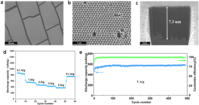
Top view observation from scanning electron microscopy (SEM) shows that blocks of SiO2 nanolattice stand on the Cu substrate, which are separated by ~5 µm width trenches (Fig. 1a). The nanolattice consists of numerous nanoscale spherical SiO2 cells, which are interconnected by through-holes and form highly ordered honeycomb architecture (Fig. 1b). From cross-sectional view, we can see about 7–10 µm thick nanolattice is intimately joined with Cu surface by filling all grooves and trenches with SiO2 cells irrespective of surface roughness (Fig. 1c).

|
Download:
|
| Fig. 1. Morphologies of the SiO2 honeycomb nanolattice and charge/discharge performances. (a) Top view of the nanolattice and (b) magnification of top view. (c) Cross-sectional view of the nanolattice and Cu substrate. (d) Discharge capacities at different rates. (e) Discharge capacity and coulombic efficiency at 1 A/g for 500 cycles. | |
Electrochemical performances were evaluated by coin-cells using lithium foil as counter electrode and the nanolattice on Cu as working electrode. As shown in Fig. 1d, the SiO2 nanolattice can discharge 1354 mAh/g under 0.1 A/g at the first cycle with initial coulombic efficiency of 70.3% (Fig. S1 in Supporting information), and it maintains above 800 mAh/g in the following cycles at 0.1 A/g. When current density increases to 5 A/g, it still can steadily offer 375 mAh/g. In 500 cycles charge/discharge at 1 A/g, the SiO2 nanolattice can steadily deliver around 575 mAh/g without obvious capacity fade, and coulombic efficiency rapidly climbs from 86% to 99% in only 16 cycles and then maintains nearly 100% to the last cycle (Fig. 1e). The typical charge/discharge profiles (Figs. 1d and e) were shown in Fig. S2 (Supporting information). Although many works on silicon-based anodes have reported excellent electrochemical performances [9], it is rare to see micron-meter thick silicon-based anode exhibit outstanding cycling stability and large reversible capacity without auxiliary of polymer binder and conductive additives. Therefore, origins of excellent electrochemical performances of the SiO2 nanolattice shall be quite different from other reported works.
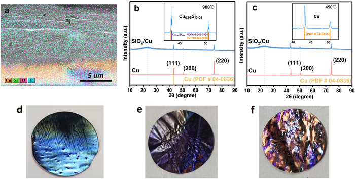
SEM-EDS mapping of the sample annealed at 900 ℃ shows that Si, Cu, O and C are heavily mixed in a region across the SiO2/Cu interface (Fig. 2a), which should be a result of vigorous interdiffusion caused by high temperature annealing. XRD pattern of the sample annealed at 900 ℃ is shown in Fig. 2b, where a small hump around 23.3° is contributed by amorphous SiO2, and there are three sharp peaks at 43.2°, 50.4°, 74.4° well match the (111), (200), (220) peaks of crystalline Cu. Interestingly, there are two additional sharp peaks adjacent to the (111) and (200) peaks of Cu (Fig. 2b inset), which perfectly match the Cu0.95Si0.05 phase. While these two peaks are absent in the sample annealed at 450 ℃ (Fig. 2c and inset). We compared interfacial adhesion force between the SiO2 nanolattice and Cu substrate by bending and rubbing the two samples 50 times. Compared to the as-prepared electrode (Fig. 2d), minor delamination presents at edge of the sample annealed at 900 ℃, while severe peeling and delamination occurs on entire surface of the sample annealed at 450 ℃ (Figs. 2e and f). Another strong evidence to confirm Cu0.95Si0.05 formation is to conduct XPS characterizations of SiO2/Cu sample (Fig. S3 in Supporting information). From the deconvolution results of Si 2p shown in Fig. S3b, three dominant peaks located at 98.8 eV, 100.6 eV and 102.7 eV can be well assigned to the Si-Cu and Si-O species, respectively [46]. Moreover, the Cu 2p XPS spectra in Fig. S3c shown two dominant peaks of 932.6 and 934.7 eV are attributed to Cu0 2p3/2 (Cu surbstrate) and CuⅡ 2p3/2 (Cu-Si) accordingly [47]. From the high-resolution XPS spectrum of O 1s, characteristic Si-O bonds can be observed at 531.4 eV. Additionally, the presence of oxygen vacancies (Ov) indicates a reduction in the valence state of Si species near the Cu0.95Si0.05 interface, consistent with the appearance of the Si2+ feature peak (Fig. S3b). Therefore, it is reasonable to conclude that the Cu0.95Si0.05 phase formed during 900 ℃ annealing firmly bonds the SiO2 nanolattice on Cu substrate, which could effectively prevent delamination of the SiO2 nanolattice from substrate under repeated stress variations.

|
Download:
|
| Fig. 2. Structure characteristics. (a) EDS mapping of the nanolattice and Cu substrate. XRD pattern of the nanolattice on Cu (b) after 900 ℃ annealing, and (c) after 450 ℃ annealing. (d) As-obtained electrode. Electrode after bending and rubbing 50 times: (e) Annealed at 900 ℃ and (f) annealed at 450 ℃. | |
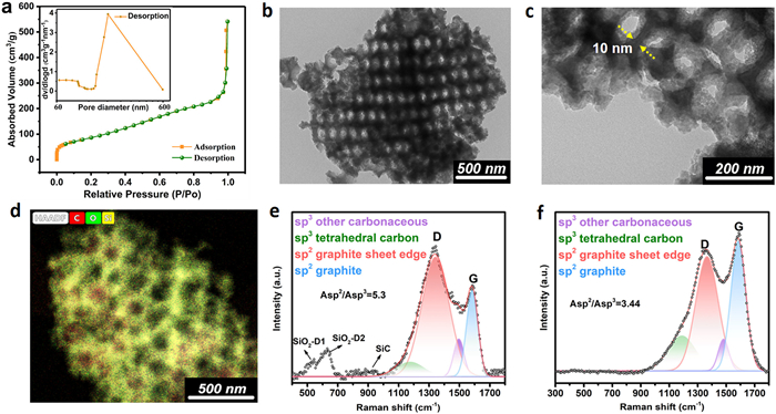
It is well-known that SiO2 shows the poorest conductivity among silicon-based anodes, and it was generally believed that large amounts of conductive additives are necessary to enhance accessible capacity of SiO2 anode [8]. While, the SiO2 honeycomb nanolattice in this work can reversibly offer more than 500 mAh/g at 1 A/g without adding additional conductive materials. To reveal origins of the large reversible capacity at high current densities, pieces of the SiO2 nanolattice were knocked off for further characterizations. Fig. 3a shows N2 adsorption-desorption isotherm of the SiO2 nanolattice, which exhibits typical H1 hysteresis loop indicating all nanoscale cells are highly uniform in size [48]. The hysteresis between adsorption and desorption is ultra-small suggesting all cells are well connected by through-holes and easy access to surrounding [48,49], which is consistent with the SEM observation (Fig. 1b). Such architecture allows facile flow of electrolyte and therefore would be benefit for homogeneous electrochemical reaction throughout the nanolattice [50].

|
Download:
|
| Fig. 3. Structure of the SiO2 honeycomb nanolattice. (a) N2 absorption/desorption curves. (b) Interconnected cells of the nanolattice. (c) Thin layer of carbon adheres on nanolattice. (d) Elements distribution shows conformal carbon coating. (e) Raman spectrum of SiO2 honeycomb nanolattice. (f) Raman spectrum of residual carbon without SiO2 honeycomb nanolattice. | |
Transmission electron microscopy (TEM) observations also show all nanoscale cells are well interconnected and each SiO2 cell is 180 nm in diameter (Figs. 3b and c), which are consistent with results of the N2 adsorption-desorption test (Fig. 3a). The wall thickness of nanoscale cell is about 10 nm, and a thin layer of carbon (5–10 nm) attaches on cell wall (Fig. 3c). The content of the carbon is only 8.7 wt% as determined by TGA test (Fig. S4 in Supporting information), which is significantly smaller than the content used in other silicon-based anodes [35]. Interestingly, high angle annular dark field (HAADF) image indicates that conformal coating of carbon on the nanolattice is achieved, which exhibits similar honeycomb pattern (Fig. 3d). Since there is no coating process involved in the synthesis, the conformal distribution of carbon hints a strong relation between the carbon and nanolattice. It has been proved that SiO2 could catalyze amorphous carbon into graphitic carbon through formation and decomposition of SiC at 900 ℃ [51–53]. Raman spectrum of the nanolattice (Fig. 3e) shows a minor hump ranging from 770 cm−1 to 970 cm−1 which is contributed by SiC [51], and D/G bands and D1/D2 bands are well-known contributed by carbon and SiO2 respectively [54]. Meanwhile, graphitization degree (Asp2/Asp3) of the carbon in the nanolattice (Fig. 3e) is much higher than that of the pyrolytic carbon derived without the nanolattice at the same annealing temperature (Fig. 3f). Therefore, it is reasonable to propose that the highly graphitic carbon is derived from catalytic graphitization occurred on the SiO2 nanolattice and maintains the similar honeycomb architecture of the nanolattice, which would greatly enhance electronic conductivity.
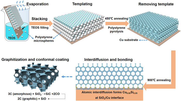
Based on above characterizations and discussions, we can draw the formation mechanism of SiO2 honeycomb nanolattice with superior mechanical stability and conductivity. As illustrated in Fig. 4, the initial honeycomb template is formed through stacking of nanosized PS balls on Cu substrate driven by evaporation of colloid suspension, and then tetraethoxysilane (TEOS) fills in and forms a reversal template. The first 450 ℃ annealing causes PS ball pyrolysis and transforms TEOS into interconnected SiO2 honeycomb nanolattice. The second 900 ℃ annealing plays two roles, on one hand vigorous interdiffusion is triggered and forms Cu0.95Si0.05 phase in the SiO2/Cu interface region; on the other hand, each SiO2 cell becomes a nanoscale reactor catalyzing pyrolytic carbon into highly graphitic carbon on cell wall. Eventually, artificial SiO2 honeycomb nanolattice with strong interfacial adhesion and superior conductivity is successfully fabricated on Cu substrate.

|
Download:
|
| Fig. 4. Illustration of fabrication process and formation mechanism of the SiO2 honeycomb nanolattice with superior conductivity and strong adhesion with Cu substrate. | |
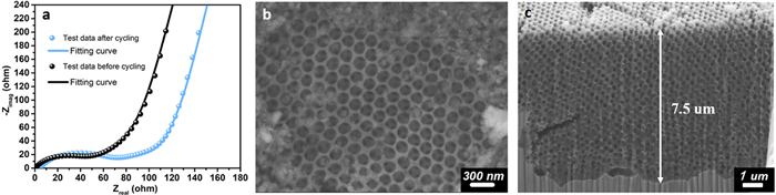
Fig. 5a displays electrochemical impedance spectra of the nanolattice anode before and after 500 cycles charge/discharge. The charge transfer resistance (Rct) is 53.9 Ω before electrochemical cycling, while it increases to 64.4 Ω after cycling. The slight increase of Rct can be ascribed to formation of stable solid electrolyte interphase (SEI) layer [31,35]. Fig. 5b shows that original spherical cells (Fig. 1b) deform significantly and become irregular oval-shaped cells, which indicates severe volume change occurred during repeated lithiation/delithiation, even so the deformed cells maintain good integrity without observable damage. From the cross-sectional view (Fig. 5c), there are two pores at the SiO2/Cu interface, and there is a crack initiated from one pore but terminated soon. Although it is unable to tell whether the crack was formed during synthesis or lithiation/delithiation, it did not cross the nanolattice after 500 cycles repeated stress variations which is a manifestation of strong crack resistance of the honeycomb architecture. Except the pores, the honeycomb nanolattice is almost seamlessly joined with the Cu substrate without distinguishable cracks after cycling, which suggests the interfacial adhesion is very stable.

|
Download:
|
| Fig. 5. Structure integrity and impedance variation. (a) Electrochemical impedance spectrum before and after cycling. (b) Top view and (c) cross-sectional view of the nanolattice after 500 cycles charge/discharge at 1 A/g. | |
This work demonstrates a facile method to fabricate SiO2 honeycomb nanolattice on Cu substrate with robust mechanical stability and excellent lithiation/delithiation performances. The initial templating process in liquid allows nanoscale SiO2 cells filling microscale grooves and trenches of Cu surface, which creates almost seamless adhesion interface irrespective of surface roughness. Furthermore, 900 ℃ annealing triggers vigorous interdiffusion and forms Cu0.95Si0.05 phase, which firmly bonds the nanolattice on Cu substrate and effectively prevents delamination under severe strain-stress variations. Inside the honeycomb nanolattice, uniform nanoscale SiO2 cells are interconnected by through-holes which allows facile flow of electrolyte throughout the 5–7 µm-meter thick anode. Moreover, conformal coating of highly graphitic carbon on the nanolattice is achieved through in situ catalytic graphitization during 900 ℃ annealing, which greatly benefits electronic conduction. This unique structure facilitates fast transportation of both Li ions and electrons and benefits homogeneous electrochemical reactions throughout the nanolattice, which results in superior reversible capacity at large current densities without auxiliary of additional binder and conductive additives. This work highlights that design and constructing artificial nanolattice can be an effective way to prevent chemo-mechanical degradation of high energy density batteries.
Declaration of competing interestThe authors declare that they have no known competing financial interests or personal relationships that could have appeared to influence the work reported in this paper.
AcknowledgmentsThis research was supported by the National Natural Science Foundation of China (Nos. 22379076, 22268033, 22108131), Natural Science Foundation of Ningxia (No. 2023AAC02009) and the Science Foundation for The Excellent Youth Scholars of Ningxia Hui Autonomous Region (Nos. 2022AAC05018, 2021AAC05002).
Supplementary materialsSupplementary material associated with this article can be found, in the online version, at doi:10.1016/j.cclet.2024.109567.
| [1] |
J. Sung, N. Kim, J. Ma, et al., Nat. Energy 6 (2021) 1164-1175. DOI:10.1038/s41560-021-00945-z |
| [2] |
B.S. Lee, S.H. Oh, Y.J. Choi, et al., Nat. Commun. 14 (2023) 150. DOI:10.1038/s41467-022-35769-2 |
| [3] |
J.D. McBrayer, M.T.F. Rodrigues, M.C. Schulze, et al., Nat. Energy 6 (2021) 866-872. DOI:10.1038/s41560-021-00883-w |
| [4] |
R. Wang, H. Li, Y. Wu, et al., Adv. Energy Mater. 12 (2022) 2202342. DOI:10.1002/aenm.202202342 |
| [5] |
Y.F. Tian, G. Li, D.X. Xu, et al., Adv. Mater. (2022) 2200672. |
| [6] |
D.H.S. Tan, Y.T. Chen, H. Yang, et al., Science 373 (2021) 1494–1499 1979.
|
| [7] |
M. Ge, C. Cao, G.M. Biesold, et al., Adv. Mater. 33 (2021) 2004577. DOI:10.1002/adma.202004577 |
| [8] |
Z. Liu, Q. Yu, Y. Zhao, et al., Chem. Soc. Rev. 48 (2019) 285-309. DOI:10.1039/C8CS00441B |
| [9] |
B. Zhu, G. Liu, G. Lv, et al., Sci. Adv. 5 (2019) eaax0651. DOI:10.1126/sciadv.aax0651 |
| [10] |
T. Wang, J. Yang, H. Wang, et al., Adv. Energy Mater. 13 (2023) 2204241. DOI:10.1002/aenm.202204241 |
| [11] |
D. Wang, T. Wang, M. He, et al., Small 17 (2021) 2103878. DOI:10.1002/smll.202103878 |
| [12] |
Z. Yan, J. Jiang, Y. Zhang, et al., Mater. Today Nano 18 (2022) 100175. DOI:10.1016/j.mtnano.2022.100175 |
| [13] |
H. Li, H. Li, Y. Lai, et al., Adv. Energy Mater. 12 (2022) 2102181. DOI:10.1002/aenm.202102181 |
| [14] |
P. Liu, B. Li, J. Zhang, et al., Chin. Chem. Lett. 34 (2023) 107946. |
| [15] |
H. Wu, P. Gao, J. Mu, et al., Chin. Chem. Lett. 33 (2022) 3236-3240. DOI:10.1016/j.cclet.2021.10.039 |
| [16] |
J. Liu, M. Ben, A. Liu, et al., Chin. Chem. Lett. 32 (2021) 2914-2918. DOI:10.1016/j.cclet.2021.02.051 |
| [17] |
T. Wang, X. Guo, H. Duan, et al., Chin. Chem. Lett. 31 (2020) 654-666. DOI:10.1016/j.cclet.2019.06.002 |
| [18] |
Q. Ouyang, G. Li, X. Liu, et al., Electrochim. Acta 426 (2022) 140772. DOI:10.1016/j.electacta.2022.140772 |
| [19] |
K. Min, K. Kim, H. An, et al., J. Power Sources 543 (2022) 231849. DOI:10.1016/j.jpowsour.2022.231849 |
| [20] |
C.B. Chang, C.Y. Tsai, K.T. Chen, et al., ACS Appl. Energy Mater. 4 (2021) 3160-3168. DOI:10.1021/acsaem.0c02932 |
| [21] |
J. Wang, J. Gao, J. Zhang, et al., Batter. Supercaps 5 (2022) e202100260. DOI:10.1002/batt.202100260 |
| [22] |
F. Wang, W. Liu, Y. Ma, et al., ACS Appl. Mater. Interfaces 12 (2021) 30668-30677. |
| [23] |
X. Liu, J. Zhu, L. Yue, et al., Small 18 (2022) 2204552. DOI:10.1002/smll.202204552 |
| [24] |
W. Weng, J. Yang, J. Zhou, et al., Adv. Sci. 7 (2020) 2001492. DOI:10.1002/advs.202001492 |
| [25] |
G. Li, Q. Shen, H. Wang, et al., ACS Appl. Energy Mater. 5 (2022) 740-749. DOI:10.1021/acsaem.1c03195 |
| [26] |
C. Wang, C. Yang, Z. Zheng, Adv. Sci. 9 (2022) 2105213. DOI:10.1002/advs.202105213 |
| [27] |
P. Li, H. Kim, S.T. Myung, et al., Energy Storage Mater. 35 (2021) 550-576. DOI:10.1016/j.ensm.2020.11.028 |
| [28] |
M. Flügel, M. Bolsinger, M. Marinaro, et al., J. Electrochem. Soc. 170 (2023) 060536. DOI:10.1149/1945-7111/acdda3 |
| [29] |
Z. Wu, Z. Wan, Z. Li, et al., Small 19 (2023) 2205065. DOI:10.1002/smll.202205065 |
| [30] |
Z. Li, G. Wu, Y. Yang, et al., Adv. Energy Mater. 12 (2022) 2201197. DOI:10.1002/aenm.202201197 |
| [31] |
H. Wu, G. Chan, J.W. Choi, et al., Nat. Nanotechnol. 7 (2012) 310-315. DOI:10.1038/nnano.2012.35 |
| [32] |
J.K. Ha, A.K. Haridas, G.B. Cho, et al., Appl. Surf. Sci. 481 (2019) 307-312. DOI:10.1016/j.apsusc.2019.03.080 |
| [33] |
J. Schlaier, S. Cangaz, S. Maletti, et al., Adv. Mater. Interfaces 9 (2022) 2200507. DOI:10.1002/admi.202200507 |
| [34] |
Z. Zhang, Z.L. Wang, X. Lu, ACS. Nano 12 (2018) 3587-3599. DOI:10.1021/acsnano.8b00703 |
| [35] |
L. Cao, T. Huang, M. Cui, et al., Small 17 (2021) 2005997. DOI:10.1002/smll.202005997 |
| [36] |
A. Mukanova, A. Jetybayeva, S.T. Myung, et al., Mater. Today Energy 9 (2018) 49-66. DOI:10.1016/j.mtener.2018.05.004 |
| [37] |
O.J. Sanumi, P.G. Ndungu, B.O. Oboirien, J. Power Sources 543 (2022) 231840. DOI:10.1016/j.jpowsour.2022.231840 |
| [38] |
J. Bauer, L.R. Meza, T.A. Schaedler, et al., Adv. Mater. 29 (2017) 1701850. DOI:10.1002/adma.201701850 |
| [39] |
H. Cheng, X. Zhu, X. Cheng, et al., Nat. Commun. 14 (2023) 1243. DOI:10.1038/s41467-023-36965-4 |
| [40] |
X. Zhang, Y. Wang, B. Ding, et al., Small 16 (2020) 1902842. DOI:10.1002/smll.201902842 |
| [41] |
X.A. Zhang, A. Bagal, E.C. Dandley, et al., Adv. Funct. Mater. 25 (2015) 6644-6649. DOI:10.1002/adfm.201502854 |
| [42] |
X. Xia, C.V. Di Leo, X.W. Gu, et al., ACS Energy Lett. 1 (2016) 492-499. DOI:10.1021/acsenergylett.6b00256 |
| [43] |
L. Baggetto, D. Danilov, P.H.L. Notten, Adv. Mater. 23 (2011) 1563-1566. DOI:10.1002/adma.201003665 |
| [44] |
E. Almog, A. Sharma, Y. Qi, J. Zimmerman, et al., Acta Mater. 225 (2022) 117552. DOI:10.1016/j.actamat.2021.117552 |
| [45] |
A.R. Garcia-Taormina, C.M. Kurpiers, R. Schwaiger, et al., Adv. Eng. Mater. 24 (2022) 2101264. DOI:10.1002/adem.202101264 |
| [46] |
J.I. Lee, Y. Ko, M. Shin, et al., Energy Environ. Sci. 8 (2015) 2075-2084. DOI:10.1039/C5EE01493J |
| [47] |
A. Shahzeydi, M. Ghiaci, H. Farrokhpour, et al., Chem. Eng. J. 370 (2019) 1310-1321. DOI:10.1016/j.cej.2019.03.227 |
| [48] |
M. Kruk, M. Jaroniec, Chem. Mater. 13 (2001) 3169-3183. DOI:10.1021/cm0101069 |
| [49] |
Q. Zhang, X.Y. Wu, K.X. Wang, et al., Chem. Eng. J. 446 (2022) 137421. DOI:10.1016/j.cej.2022.137421 |
| [50] |
S. Li, G. Tian, R. Xiong, et al., Energy Storage Mater. 46 (2022) 443-451. DOI:10.1016/j.ensm.2022.01.035 |
| [51] |
A. Bachmatiuk, F. Borrnert, M. Grobosch, et al., ACS Nano 3 (2009) 4098-4104. DOI:10.1021/nn9009278 |
| [52] |
X. Li, M. Chi, S.M. Mahurin, et al., Carbon 101 (2016) 57-61. DOI:10.1016/j.carbon.2016.01.043 |
| [53] |
H. Liu, W. Zeng, Y. Yang, et al., J. Mater. Chem. A 9 (2021) 1260-1268. DOI:10.1039/D0TA10179F |
| [54] |
T. Yamada, M. Nakajima, T. Suemoto, et al., J. Phys. Chem. C 111 (2007) 12973-12979. DOI:10.1021/jp072312v |