 2020, Vol. 31


b Hunan Key Laboratory of Super Microstructure and Ultrafast Process, School of Physics and Electronics, Central South University, Changsha 410082, China;
c Key Laboratory for Organic Electronics and Information Displays & Institute of Advanced Materials (IAM), Nanjing University of Posts & Telecommunications, Nanjing 210023, China;
d Key Laboratory of Materials Processing and Mold (Zhengzhou University), Ministry of Education, Zhengzhou University, Zhengzhou 450002, China
Hybrid organic–inorganic perovskite have recently emerged as a prospective class of materials for efficient conversion of solar energy. The typical hybrid organic–inorganic perovskite possess excellent properties as follows: (1) High absorption coefficient and broad absorption spectrum almost covering the whole visible region from 300 nm to 800 nm for MAPbI3 [1], with blue-shift after Cl/Br doping for MAPbXyI3-y (X = Br, Cl) [2], redshift for FA doping for (FA)x(MA)1-xPbI3 [3] and tin (Sn) substitution of Pb [4], especially enormous redshift for MASnI3 [5], MASnxPb1-xI3 [5], FASnI3 [6], (FA)1-x(MA)xSnI3 [7] and (FA)1-x(MA)xSnxPb1-xI3 [8] beyond 1000 nm; (2) ambipolar charge-transport capabilities with high charge carrier mobility of MAPbI3 as high as 5-12 cm2 V-1 s-1 for electrons and that for holes within 1-8 cm2 V-1 s-1 [9, 10]; (3) large and relatively balanced electron and hole diffusion lengths which can reach micrometer order for MAPbI3, MAPbClxI3-x and (FAI)x(MABr)1-xPbI2 [11-13]; (4) almost all photo-generated excitons of perovskite can be thermally dissociate under normal operating temperatures, the perovskite/electron-transporting layer interface and the perovskite/hole-transporting layer is not essential for the exciton separation in a perovskite cell [14-18]. The perovskite layer can not only function as light harvester but also as electron-transporting material or hole-transporting material at the same time. These properties enable this type of materials to be great potential light-harvesting active materials in photodetector, light-emitting diode, photovoltaic cells, photocatalysis, etc. Here, we summarize the recent progress of hybrid organic–inorganic perovskite for photodetector, light-emitting diode, photovoltaic cells, photocatalysis. The challenges and perspectives for the hybrid organic–inorganic perovskite-based photodetectors, light-emitting diodes, solar cells and photocatalysts are considered.
2. Perovskite photodetectorsIn the past few years, organic–inorganic hybrid perovskite and all inorganic perovskite have attracted enormous attention in many optoelectronic fields, including light-emitting diode (LED), photodetector (PD), solar cells, semiconductor lasers and field effect transistors, because of their excellent photoelectric and electrical properties [19-34]. Among these fields, the PDs, converting incident light into electrical signal, are critical to various scientific and industrial applications, including military, optical communications, space exploration, and bio-sensor [35-37]. Up to now, a large number of semiconductor materials have been developed for the emerging PD applications [38, 39]. Although these materials are very promising, relatively expensive synthesis methods may greatly hinder their wide applications [40]. Therefore, organic–inorganic hybrid perovskites have shown growing interests for the development of high-performance PDs due to their high absorption coefficients, long-range electron and hole transport lengths, and direct bandgaps [41]. Herein, the progresses of this hot field are introduced as bellows.
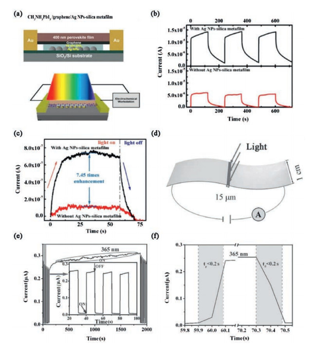
2.1. Inorganic/organic perovskite photodetectorsGraphene is a promising photoelectric material with high carrier mobility and chemical stability [42]. The combination of graphene and perovskite can obtain an excellent photoelectric detection performance [42]. A new device structure by implementing an Ag nanoparticles-embedded SiO2 (Ag NPs–silica) metafilm as the substrate of perovskite/graphene PD is reported by Liu et al. (Fig. 1a) [43]. Organic–inorganic hybrid CH3NH3PbI3 perovskite films were prepared on top of the graphene. The channel region of active devices was determined by two Au electrodes. Ag metal NPs were embedded in a 10-nm-thick SiO2 layer underneath the graphene channel. The local surface plasmon resonance on the embedded Ag NPs can generate a strong enhanced evanescent electromagnetic field to enhance the absorption of perovskite. The 10-nm thick SiO2 superlayer separates the Ag NPs below from the perovskite layer to inhibit the transfer of harmful charge and energy from perovskite to Ag NPs, so as to achieve the best effect of plasma light capture. An experimental apparatus for light response measurement can be found in bottom panel of Fig. 1a. The dynamic light response (585 nm, 1.27 × 10⁻⁶ W) measured on graphene/perovskite heterojunction PDs is shown in Fig. 1b. Black and red lines represent the light response of 120 s with and without plasmonic Ag NPs–silica metafilm, respectively. Repeatable dynamic response modes can be clearly observed for these two devices, which indicates the stable light detection of the device is obtained. An enlarged view of a 60 s on/off response period measured under 585 nm illumination with a power of 2.51 ×10⁻⁶ W is shown in Fig. 1c. Interestingly, the photo-response of perovskite/graphene PDs on the Ag NPs–silica metafilm is 7.45 times higher than that of perovskite/graphene PDs without metafilm. It is understood that this enhancement factor is the highest in all reports using an integrated NPs strategy for perovskite PDs [43]. Another important type of PD is demonstrated by Hu et al. (Fig. 1d) [44]. CH3NH3PbI3 (MAPbI3) film deposited on indium-tin oxide (ITO) electrodes with bridging-gap length of 1 cm and width of 15 μm, respectively. Fig. 1e shows photocurrent response of the PD to monochromatic light in the ultraviolet and visible range. The average photocurrent over 2000 s is about 0.25 μA, and no obvious degradation is detected, which indicates that the sensor based on MAPbI3 exhibits a good photocurrent stability. The inset of Fig. 1e is the enlarged portion of 20-100 s range. The transient photocurrent of this device with more details can be found in Fig. 1f. In general, the rise time and decay time of PDs are defined as the time for the peak current increases to 90% of the initial current, or vice versa. For this device, the decay time and rise time are both shorter than 0.2 s. Fast response speed and excellent stability of this device hold high promise for the emerging PD applications.

|
Download:
|
| Fig. 1. (a) Schematic structure of a perovskite/graphene heterojunction photodetector on the Ag NPs–silica metafilm, experimental setup for photoresponse measurement. (b) Dynamic photoresponse of perovskite/graphene heterojunction photodetectors with (black) and without (red) an Ag NPs–silica metafilm. (c) Amplified view of one cycle of photoresponse of perovskite/graphene heterojunction photodetectors. (d) Schematic illustration of the MAPbI3 film photodetector. (e) Photocurrent response of the photodetector to monochromatic light in the ultraviolet and visible range. (f) The more detailed transient photocurrent of this device. (a–c) Reproduced with permission [43]. Copyright 2019, American Chemical Society. (d–f) Reproduced with permission [44]. Copyright 2014, Wiley. (For interpretation of the references to color in this figure citation, the reader is referred to the web version of this article.) | |
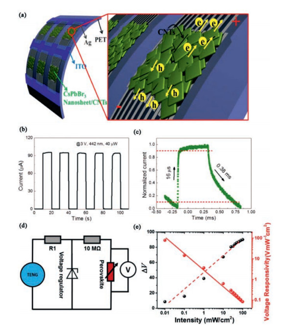
Flexible PDs are widely used in portable and wearable devices due to their low cost and weight [24, 45]. Recently, the flexible perovskite PDs based on CsPbBr3 nanosheet/carbon nanotubes (CNT) composite films are reported by Li et al. [46]. Fig. 2a shows a schematic diagram of the device structure in which an active composite film is deposited on a flexible substrate by drop casting approach. When the voltage is applied, the photo-carriers are quickly separated and transferred to the electrode as shown on the right panel. The 442 nm light was applied during the measurement to show the photo-switching behavior of the CNT-doped PDs. Fig. 2b shows I-t curve of the PD (3 V, 40 μW). When the light is turned on, the current rises sharply to be 100 μA. The current falls fast when the light is turned off, implying that the fast response of the PDs is observed. The response speed can be also measured by a continuous 442 nm laser light (Fig. 2c). From this figure, it is clearly estimated that the decay and rise times were 0.38 ms and 16 μs respectively, which are much shorter than those reported in two-dimension (2D) lead halide perovskites nanosheet based devices [47].

|
Download:
|
| Fig. 2. (a) Schematic illustration of the flexible PD and enlarged schematic illustration of the film. (b) I–t curve of the PD. (c) Rise and decay time of the device at a frequency of 500 Hz. (d) Equivalent circuit diagram of the device. (e) The change in the measured voltage (ΔV) and voltage responsivity of the device at different light intensities. (a–c) Reproduced with permission [46]. Copyright 2017, American Chemical Society. (d–e) Reproduced with permission [48]. Copyright 2017, Wiley. | |
In addition to flexible perovskite PDs, self-powered PDs are also highly desirable for applications in smart building, optical communications, and image sensing [2, 3]. Recently, a self-powered and flexible PD based on the methylammonium lead iodide (CH3NH3PbI3) perovskite is reported by He et al. [48], and the equivalent circuit diagram is shown in Fig. 2d. When the light absorbing perovskite is irradiated by light, the generated photocarriers will reduce the resistivity. Therefore, the voltage generated by triboelectric nanogenerators (TENGs) is separated by the perovskite and a 10 MΩ resistor, and the electric potential difference of perovskite decreases. It is worth noting that self-powered PD can work quantitatively and continuously even driven by irregular motion, thus avoiding the need for large motion actuators. The changes of device voltage (ΔV) and voltage response rate can be found in Fig. 2e, which are defined as 

In recent years, organic–inorganic halide perovskite materials have attracted many attentions because of their excellent properties of electronic and photoelectric properties [49-51]. The efficiency of perovskite-based solar cells has been greatly improved from 3% to 22.1% [52]. In addition to solar cells, light-emitting diodes (LED) also represents a wide range of applications of halide perovskite materials, including in optical communication, medical science and display technology [20, 21]. Therefore, it is necessary to make a brief introduction to the recent developments of perovskite-based LED.
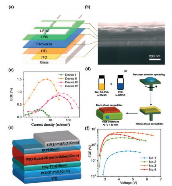
2.4. Low-dimensional perovskites light-emitting diodesThe traditional metal halide perovskite (MHP) has three-dimensional (3D) structure with a chemical formula of AMX3 (A = CH3NH3 (MA), Cs; M = Pb, Sn; X = Cl, Br, I). Recently, by separating 3D inorganic octahedral network, a quasi-2D perovskite material with reduced size domain was developed [53]. Xing et al. reports color-stable sky blue perovskite LEDs obtained by enhancing the phase monodispersity of quasi-2D perovskite films [54]. The device structure and cross-sectional scanning electron microscope (SEM) image are shown in Figs. 3a and b, respectively. In order to investigate the influence of the thickness on the device performance, the perovskite LEDs with the active layer thickness ranging from 125 nm (Device Ⅰ) to 80 nm (Device Ⅱ), 60 nm (Device Ⅲ), and 40 nm (Device Ⅳ) are fabricated. The best external quantum efficiencies (EQEs) about 1.5% (Device Ⅱ) can be found in Fig. 3c, which is governed by exciton and charge carrier dynamics. Another type of quasi-2D perovskite LED is demonstrated by Tian et al. [55]. Fig. 3d shows the preparation process of luminescent quasi-2D perovskite/PEO composite films. Blending metal halide perovskite with polymer is an effective way to improve the performance of perovskite based optoelectronic devices. The structure of the device is shown in Fig. 3e, where tris-1-phenyl- 1-H-benzimidazole (TPBi) is electron transport layer, poly(3, 4-ethylenedioxythiophene)-polystyrene sulfonate (PEDOT:PSS) is hole injection layer, and poly(4-butylphenyl-diphenyl-amine) (poly TPD) is hole electron/transport block layer, respectively. The EQEs corresponding to different composite films is shown in Fig. 3f. Interestingly, a high EQE value of 6.23% has been obtained based on the composite thin film No. 3, which is the highest value for red perovskite LEDs.

|
Download:
|
| Fig. 3. (a) Device structure of perovskite LEDs. (b) Cross-sectional SEM image of the perovskite LEDs. (c) EQE-current density. (d) Processing of quasi-2D perovskite/PEO composite thin films. (e) The structure of the LED. (f) EQE versus voltage. (a–c) Reproduced with permission [54]. Copyright 2018, Springer. (d–f) Reproduced with permission [55]. Copyright 2018, Wiley. | |
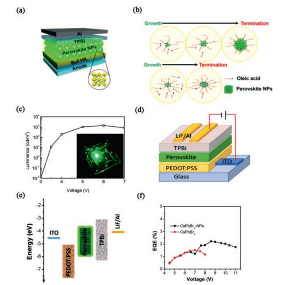
Zero dimension (0D) perovskite-based colloidal nanocrystals (NCs) CsPbX3 (X=Cl, Br and I) is another type of perovskite with good light-emitting performance [56]. Based on the colloidal perovskite NCS, high efficiency LEDs with size >DB (Bohr diameter) has been reported by Kim et al. [57]. Fig. 4a shows the device architecture of perovskite nanoparticles LEDs where Buf-HIL is a multifunctional buffer hole injection layer. The size of perovskite nanoparticles can be controlled by adjusting the amount of oleic acid (Fig. 4b). By increasing the thickness of emitting layer to ~30 nm, the luminous efficiency of NC-LEDs can be further optimized. The perovskite NC-LEDs exhibits a very bright green emission (Fig. 4c). Furthermore, a high EQE value of 5.09% has been obtained, which is the best performance in green LEDs based on colloidal organic–inorganic metal-halide perovskite nanoparticles. Another new type of perovskite LED using all-inorganic CsPbBr3 nanoparticles composite nanocrystals as emitting layer has been reported by Zhang et al. [58]. The structure of multilayer all-inorganic CsPbBr3 nanoparticles perovskite LED is shown in Fig. 4d. The flat-band energy level of device is shown in Fig. 4e, where the TPBi and PEDOT:PSS are employed as electron and hole transport layers, respectively. Compared with single CsPbBr3, the CsPbBr3 and CsPb2Br5 nanoparticle composites can further achieve a larger EQEs value of about 2.21%, as shown in Fig. 4f. Basically, the introduction of CsPb2Br5 nanoparticles can improve the ionic conductivity and emission lifetime by reducing the potential barrier of electron and ion transport. Biphasic all inorganic CsPbBr3 nanoparticle and nanocrystal composite would provide a new perovskite material path for the advanced light-emission applications.

|
Download:
|
| Fig. 4. (a) Device architecture of perovskite nanoparticles-LEDs. (b) Schematic illustration of size-controllable perovskite nanoparticles synthesis. (c) Luminance characteristics and photograph (inset) of perovskite NC-LEDs. (d) The structure of multilayer all-inorganic CsPbBr3 nanoparticles perovskite LEDs. (e) The diagram of flat-band energy level. (f) EQE as a function of voltages. (a–c) Reproduced with permission [57]. Copyright 2017, American Chemical Society. (d–f) Reproduced with permission [58]. Copyright 2016, Wiley. | |
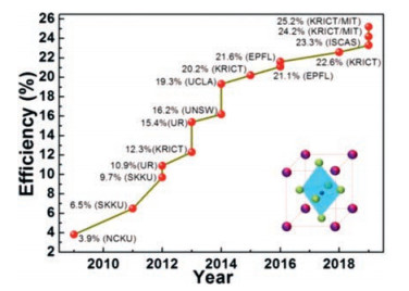
Hybrid organic–inorganic perovskite, a hybrid organic–inorganic lead (Pb) (or tin (Sn) or binary Pb/Sn) halide-based compounds with ABX3 perovskite structure [59], not only possess strong capacity of light absorption and high efficiency of photoninduced carrier generation but also excellent dual-carrier (hole and electron) transport ability. These special photoelectric characteristics endow perovskite materials with great potential as photoactive materials in photovoltaic cells. In addition, the simple chemical composition and facile fabrication processes of the perovskite layer, significantly reduces the costs of whole device fabrication and minimizes the barrier to entry of this field, exhibiting huge advantages than silicon (Si) solar cells, copper indium gallium diselenide (CIGS) solar cells and organic solar cells (OPV), etc. [4]. Therefore, many researchers have participated in this research field to explore many species of materials and technologies to advance the development of perovskite solar cells (PSCs), with most conspicuous syndrome of continuous break-through in efficiencies. As shown in Fig. 5, since 2012 [60, 61], PSCs have undergone tremendous development and power conversion efficiency (PCE) greater than 25% [62-70] has been achieved through structural evolution of device [4, 59, 71, 72], perovskite crystalline engineering [2, 13, 65, 73-79] and interfacial engineering [4, 62, 80-94], making this a fastest-advancing solar technology to date. Among these issues, the first that to be discussed is, the structural evolution of the PSC device, which has evolved from initial solid–liquid type known as dye-sensitized solar cells [95, 96], to all-solid-state type [60, 61] which is exactly referred to PSCs currently. The all-solid-state typed structure was further simplified from mesoscopic heterojunction type to planar heterojunction p-i-n type [97, 98]. On this basis of the structure modification, plenty of perovskite crystalline engineering strategies consisting of two aspects, the selection of deposition patterns and regulation of composition, were implemented to facilitate the perovskite film deposition process and quality. The deposition patterns involve single-step solution deposition including direct spin-coating [99, 100] and one-step rapid crystallization by adding anti-solvent in the early stage of spin-coating [73, 101], two-step sequential dipping (or spin coating) method [102, 103], dual source vapor deposition [97] vapor-assisted solution method [104] and acetic acid assisted crystallization method [105]. The regulation of composition was realized by adjusting the chemical element composition of perovskite materials, mainly adopting introduce of FA, Cs cation [106-108] and Br, Cl anion [2, 61] to partially substitute MA cation and I anion respectively, which produce more excellent perovskite materials with superior stability, light-absorption, charge mobility and life-time. Besides structure and perovskite material aspects, interfacial engineering has been considered as one of most effective approaches toward highly efficient PSCs, through which the carrier extraction and transport from perovskite layer to electrodes can be greatly enhanced [82, 109]. Except that used in other types of solar cell like OPV, a lot of novel and specific interfacial materials for PSCs have emerged, including hole transporting materials (HTMs) [62, 83-85], electron transporting materials (ETMs) [89-95], passivation materials of perovskite [65, 110-115], and modification materials of electrode [116-121]. Widely used HTMs fall into two categories: inorganic such as NiOx, CuOx, CuSCN, CuI, V2O5, etc. [4, 83, 85]. and organic semiconductors, which can be subdivided into small molecules and polymers [4, 62, 83, 84, 88]. Small molecules are represented by spiro-OMeTAD, pyrene-core arylamine derivatives, arylamine derivatives, and donor materials in OPV, while polymers are commercial PEDOT:PSS, P3HT, and later developed polythiophene derivatives, poly(triarylamine) derivatives, and donor material in OPV. Similar with HTMs, ETMs can also be classified into inorganic semiconductors primarily TiO2, ZnO, SnO2 and organic semiconductors subdivided into small molecules and polymers [89, 81-94]. The ETMs of small molecules include fullerene derivatives like C60, PCBM, bis-C60, and naphthalimide, perylene-bisimide, azaacene-based derivatives, as well as fused-ring electron acceptors. On the other hand, the ETMs of polymers are naphthalimide-thiophene, naphthalimide-thiophene, perylene-bisimide-based copolymer derivatives, and so on. Usually, single layer of HTM or ETM cannot function very well to achieve high efficiency, therefore bilayer or tri-layer of HTM or ETM were applied. Other desirable materials were also exploited, consisted of passivation materials inserted between perovskite layer and interfacial layer, and modification materials for electrodes, which act on identical effects, forming selective contact between perovskite layer with electrode layer for more smooth charge transfer, reducing charge recombination and thus improving device performance [122-124].

|
Download:
|
| Fig. 5. Efficiency roadmap for perovskite solar cells: efficiency values taken from publications and NREL's latest chart on record cell efficiencies. | |
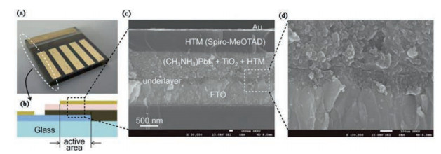
The prototype of present PSCs origins from organo-metal nanocrystals sensitized-TiO2 for solar cells reported by Tsutomu Miyasaka group in 2009 adopting structure to achieved 3.9% efficiency [96]. In 2011, Nam-Gyu Park group improved the efficient of this perovskite quantum-dot-sensitized solar cell to 6.5% [95]. However, a fatal defect of these devices was that electrolyte solution would damage the perovskite materials and lead to a rapid degradation of solar cell. To overcome this shortcoming, in 2012, Nam-Gyu Park group implemented a milestone structure innovation forPSCs [60]. Anall-solid-state mesoscopic heterojunction solarcells were constructed featuring FTO/compact-TiO2/mesoscopic-TiO2/CH3NH3PbI3/2, 2', 7, 7'-tetrakis-(N, N-di-p-methoxyphenyl-amine)- 9, 9'-spirobifluorene (spiro-MeOTAD)/Au configuration (Fig. 6) and 9.7%PCE with much better stability was obtained [60]. In 2013, Henry J. Snaith group developed the traditional mesostructured TiO2 or Al2O3, and a relatively simple planar heterojunction p-i-n solar cell was successfully constructed to give a 15.4% efficiency [61]. On basis of the regular structure of FTO/ETL/perovskite/HTM/Metal discussed above, the inverted device structure of ITO/HTM/CH3NH3PbI3/ETM/metal was first reported by Tzung-Fang Guo group in 2013 [98]. This cell of ITO/poly(3, 4-ethylenedioxythiophene)polystyrene sulfonate (PEDOT:PSS)/CH3NH3PbI3/C60(or phenyl-C61-butyric acid methyl ester (PC61BM)/ bathocuproine(BCP)/ aluminum(Al) achieved a decent efficiency of 3.9% [98].

|
Download:
|
| Fig. 6. Solid-state device and its cross-sectional meso-structure. (a) Real solid-state device. (b) Cross-sectional structure of the device. (c) Cross-sectional SEM image of the device. (d) Active layer-underlayer-FTO interfacial junction structure. (a–d) Reproduced with permission [60]. Copyright 2012, Springer. | |
In 2014, Sang Ⅱ Seok group described the compositional engineering of (FAPbI3)1-x(MAPbBr3)x for efficient PSCs [73]. Optimized perovskite composition of (FAPbI3)0.85(MAPbBr3)0.15 proves many advantages over the systems of MAPbI3, FAPbI3, and MAPb(I0.85Br0.15)3, which enhances the PCE for more than 18%. This strategy gives major implications for the subsequent research on improving PSC efficiency via adjustment of perovskite chemical components. In 2015, Sang Ⅱ Seok group reported an approach to depositing high-quality FAPbI3 films with large-grained dense microstructures and flat surfaces without residual PbI2, by the direct intramolecular exchange of dimethylsulfoxide (DMSO) molecules intercalated in PbI2 with formamidinium iodide, resulting in an efficiency greater than 20% [125]. In 2016, Michael Grätzel group added small amounts of inorganic cesium (Cs) or rubidium cation (Rb+) in a "triple cation" (Cs/MA/FA or Rb/MA/FA) configuration to obtain more pure perovskite films with highly monolithic grains [126], through which method, efficiencies up to 21.1% and 21.6% (stabilized) were achieved, respectively. In 2018, Jang won Seo group synthesized a fluorene-terminated HTM with a fine-tuned energy level and a high glass transition temperature, to realize a champion device of 23.2% efficiency (under reverse scanning) with a steady-state and certified efficiencies of 22.85% and 22.6%, respectively [62]. In 2019, Jingbi You group and Michael Grätzel group respectively reported the utilization of an organic halide salt phenethylammo-nium iodide (PEAI) or pentafluoro-phenylethylammonium (FEA) inserted between the 3D perovskite and HTM to passivate surface defect of perovskite and suppress non-radiative recombination, contributing to the enhanced efficiencies [65]. In this way, a certificated record efficiency of 23.32% (quasi-steady state) is created by You's group. In 2019, Moungi G. Bawendi group developed a selective precursor dissolution (SPD) strategy, that is employing a unique precursor/solvent combination (linear alkyl ammonium bromides/chloroform) for to build a layered perovskite (LP) onto an underlying 3D perovskite film [67]. This LP can effectively passivate interface and grain boundary defects, increase moisture resistance, and outperform state of the art single layer 3D devices, leading to a striking PCE of 22.6%. Dong Suk Kim group systematically investigated the effects of MACl addition into FAPbI3 perovskite, and the highest PCE achieved was 24.02% based on the optimal perovskite composition, certified as 23.48% [64]. These excellent efficiencies had been exceeded subsequently, reaching as high as about 25%. Current PSC performance seems to approach the limit of its single-junction solar cells, and higher efficiencies than this record is hard to achieve, which could still be expected through adjusting perovskite composition to increase the light-harvesting ability, exploring more efficient interfacial materials or constructing tandem structure. Although the efficiency is no longer an obstacle to commercial production of PSCs, however, another thorny issue about the device stability must be solved before the actual application of PSCs.
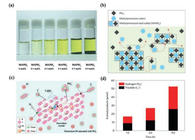
4. Hybrid organic/inorganic perovskite photocatalysts 4.1. Photocatalytic hydrogen evolution reactionThe first hybrid organic–inorganic perovskite of methylammonium lead iodide (MAPbI3) was applied in photocatalytic hydrogen evolution reaction (pHER) by Park et al. [127]. Their experimental results identified that pHER from high concentration electrolyte of hydriodic acid (HI) solution is feasible (Fig. 7a). Compared with the unstable MAPbI3 in the water, the dynamic equilibrium between HI solution and MAPbI3, leading to the stable phase of MAPbI3 (Figs. 7b and c). Peter C.K. Vesborg point out, however, the triiodide product competing in absorbing the incoming light with the proton H+ (Fig. 7d) [128]. Even so, lots of researchers have tried their best to exploit and develop the applicable HI solution methods for pHER. Wu et al. reported that the composite of MAPbI3 with reduced graphene oxide (rGO) is an outstanding visible-light pHER catalyst in saturated HI solution with MAPbI3 [129]. The specific electron transfer mechanism from MAPbI3 to rGO sites is the key to the excellent pHER performance in the HI solution than that of pristine MAPbI3. Moreover, the composites revealing the highly stability in the repeated pHER experiments. Wang et al. considered that the MAPbI3 will affect the light adsorption of the black nature of rGO. Thus, choosing a more suitable candidate with minor influence on light adsorption is important for the electron transportation. They reported the composite of Pt/TiO2 and MAPbI3 can effectively enhance charge transportation between MAPbI3 and TiO2 [130]. And the Pt anchored in the TiO2 can be as the pHER cocatalyst to improve the catalytic performance. Li et al. reported a photocatalytic H2 evolution catalyst of MAPbBr3 nanocrystals, which can be stabilized in HBr solution [131]. Further, the hybridizing MAPbBr3 with Pt/TaO5 and poly(3, 4-ethylenedioxythiophene) polystyrene sulfonate (PEDOT: PSS) can effectively enhance the H2 evolution performance under the visible light. Moreover, the mixed halide perovskite can also adjust the charge carriers to enhance the pHER. Wu et al. adopted the mixed-halide MAPbBr3-xIx/Pt to enhance photocatalytic activity for pHER under visible light. The 250 mg catalysts exhibited a photocatalytic H2 evolution rate of 651.2 μmol/L and a solar-to-chemical conversion efficiency of 1.05%. Similarly, Zhao et al. reported a stable hybrid perovskite MAPb(I1-xBrx)3 for pHER in HX solution [132]. The optimized MAPb(I1-xBrx)3 (x = 0.10) shows a highest H2 evolution rate of 1471 μmol h-1 g-1 under visible light. It is important to develop theoretical and experimental methods to reveal the mechanism of hybrid organic–inorganic perovskite in HX solution for pHER.

|
Download:
|
| Fig. 7. (a) MAPbI3 in different concentration of aqueous HI solution. (b) The dynamic equilibrium mechanism of MAPbI3 in a saturated HI solution. (c) Schematic diagram of photocatalytic hydrogen evolution reaction by using MAPbI3 in aqueous HI solution. (d) Quantitative comparison between the H2 and I3- at different reaction times. (a–c) Reproduced with permission [127]. Copyright 2017, Springer. (d) Reproduced with permission [128]. Copyright 2017, Springer. | |
It is a great challenge for hybrid organic–inorganic perovskite to catalyze H2 production in an aqueous solution under visible light. Recently, Ju et al. reported that DMASnI3 (DMA = CH3NH2CH3+) exhibit excellent water phase stability [133]. Experimental results identified that the DMASnI3 can maintain the initial phase structure in the deionized water with 16 h. The pure DNASnI3 crystals have the good recycling properties with a photocatalytic H2 evolution rate of 0.64 μmol/h. Similarly, Pisanu et al. reported the DMASnBr3 crystals have a stable phase structure in deionized water [134]. Moreover, under visible light, the DMASnBr3 exhibited an effectively H2 production performance with a rate of 6 μmol/h. Designing stable hybrid organic–inorganic perovskite and improving the H2 production rate may be needed detail and in-depth investigation.
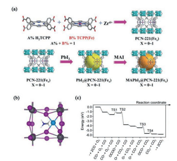
4.2. Photocatalytic CO2 reduction reactionMore recently, the hybrid organic–inorganic perovskite have been adopted in the photocatalytic CO2 reduction reaction [135-137]. Wu et al. reported that the MAPbI3 perovskite quantum dots (QDs) protected by the metal organic framework (MOF) PCN- 211(Fex) exhibiting stable phase structure in reaction systems containing water (Fig. 8a) [135]. The composite systems exhibited a high total yield of 1559 μmol/g or photocatalytic CO2 reduction, which can be ascribed to the rapidly transfer of photogenerated electrons in the QDs to the Fe active sites in the MOF. Wang et al. adopted graphene oxide (GO) wrapped MAPbBr3 perovskite QDs for photoelectrochemical CO2 reduction in nonaqueous media [136]. The perovskite QDs can be protected by the GO and serve as electron transport medium to separate photoinduced electrons and holes. Remarkably, Fu et al. predicted that the hybrid organic–inorganic perovskites can be as the substrates for Pt single-atom catalysts for CO2 reduction reaction and CO oxidation (Fig. 8b) [137]. The first principle computational results revealed that the Pt exhibits a higher adsorption energy than MA, suggested the exothermic adsorption of Pt in replacing the MA species on the surface of (110) and (001) substrates. The reaction pathway and free-energy profile of the catalytic CO oxidation at Pt1@(110) shows that the reaction rate-determining step is the adsorbed O2 and CO molecule combine into OCOO complex with an endothermic of 0.58 eV (via TS1) (Fig. 8c). The formation of CO2 has the negative charge of 0.55 e- demonstrate the activation of CO2, suggesting the applicable CO2 reduction reaction on the substrate. These findings demonstrated that the hybrid organic–inorganic perovskites have the potential application as the photocatalytic CO2 reduction catalysts. The hybrid organic–inorganic perovskites not only have the suitable band gaps for harvesting sunlight, and exhibit high optical adsorption, high charge-carrier lifetimes and long diffusion lengths. Thus, the hybrid organic–inorganic perovskite is the promising candidate as photocatalysts for HER, CO2RR, ORR, N2RR and etc.

|
Download:
|
| Fig. 8. (a) Schematic diagrams for the synthesis of PCN-221(Fex) and MAPbI3@PCN-221(Fex). (b) Optimized geometry structure of Pt1@(110). (c) free-energy diagram of CO oxidation at the Pt1@(110) substrate. (a) Reproduced with permission [135]. Copyright 2019, Wiley. (b and c) Reproduced with permission [137]. Copyright 2019, American Physical Society. | |
Up to now, a large variety of inorganic/organic perovskite PDs with impressive photoresponse performance have been realized. Flexible and self-powered perovskite PDs are widely used in portable and wearable devices. Although remarkable achievements have been made in this field, there are still some critical challenges in the future development of hybrid PDs, such as ion migration, intrinsic instability of organic–inorganic hybrid perovskite and some incorporation of toxic element etc. [138, 139]. Therefore, in the future work, more efforts are needed to understand the basic characteristics of materials and develop new process technologies for this kind of devices.
Perovskite not only has been successfully applied in photovoltaics and LEDs, but also has a broad application prospect in future display and lighting technologies due to its wide range of color tunability, high quantum yield, narrow photoluminescence and low-cost fabrication process [40, 41, 140-144]. Although the efficiency of devices has reached a competitive level, long-term solutions are still needed due to the challenges of the moisture and thermal stability, the feasibility of large-scale manufacturing, and the toxicity of Pb, etc. [36, 43, 44, 47, 145-147]. Therefore, new strategies are still needed to improve the stability of perovskite LEDs and investigate Pb-free LEDs in the next few years.
PDs have inspired tremendous attention and extensive research, due to the peculiar electronic and optical properties of perovskite semiconductor materials. PDs performance can be improved by: (ⅰ) The engineering of interface layer and device structure, (ⅱ) the synthesis of varying morphology perovskite active layers and (ⅲ) the construction of a heterojunction between perovskite materials and inorganic (or organic) materials. Despite the great progress of perovskite PDs, there is still room to further improve the PDs performance and extend its response spectrum. For example, the broadband perovskite PDs of spectral response ranging from ultraviolet to short-wave infrared can be achieved by combining perovskite materials with other semiconductor materials. Before the real applications, the challenges of toxicity and stability issues should be well addressed for the further development of perovskite PDs. These issues can be solved via the development of chemically stable leadfree perovskite materials. All in all, perovskite PDs is a promising device for various scientific and industrial applications including military, optical communications, space exploration and biosensors.
Perovskite based solar cells have achieved tremendous process in conversion efficiency, whereas their stability and toxicity stemming from lead element, still lie across the application of this photovoltaic technique since its birth. Although many methods such as designing novel interfacial materials and adding Cs element to enhance the stability of perovskite layer through preventing entering of water or the migration of iodine ions, or improvement of perovskite crystalline, have been demonstrated that can improve the stability of devices at some extent, it cannot compare with other photovoltaic techniques such as silicon, CIGS, even OPV. On the other side, lead-free perovskite solar cells, mainly Sn-based ones, develop very slowly, displaying much inferior efficiency. Therefore, better strategies are expected such as rising all-inorganic, or 2D-3D structural perovskite solar cells.
Additionally, it's in its infancy for the hybrid organic–inorganic perovskite materials as the photocatalyst. Different strategies and methods are still needed to be designed to enhance the catalytic activation and the stability of hybrid organic–inorganic perovskite materials in the further.
Declaration of competing interestThe authors declare that they have no known competing financial interests or personal relationships that could have appeared to influence the work reported in this paper.
AcknowledgmentsThis work was supported by the National Natural Science Foundation of China (Nos. 11675051, 51302079, 51702138), the Natural Science Foundation of Hunan Province (No. 2017JJ1008), and the Key Research and Development Program of Hunan Province of China (No. 2018GK2031).
| [1] |
N.G. Park, Mater. Today 18 (2015) 65-72. DOI:10.1016/j.mattod.2014.07.007 |
| [2] |
N.J. Jeon, J.H. Noh, W.S. Yang, et al., Nature 517 (2015) 476-480. DOI:10.1038/nature14133 |
| [3] |
S. Pang, H. Hu, J. Zhang, et al., Chem. Mater. 26 (2014) 1485-1491. DOI:10.1021/cm404006p |
| [4] |
W. Yan, S. Ye, Y. Li, et al., Adv. Energy Mater. 6 (2016) 1600474. DOI:10.1002/aenm.201600474 |
| [5] |
S.D. Stranks, H.J. Snaith, Nat. Nanotechnol. 10 (2015) 391-402. DOI:10.1038/nnano.2015.90 |
| [6] |
X. Meng, J. Lin, X. Liu, et al., Adv. Mater. 31 (2019) 1903721. DOI:10.1002/adma.201903721 |
| [7] |
Z. Zhao, F. Gu, Y. Li, et al., Adv. Sci. 4 (2017) 1700204. DOI:10.1002/advs.201700204 |
| [8] |
R. Lin, K. Xiao, Z. Qin, et al., Nat. Energy 4 (2019) 864-873. DOI:10.1038/s41560-019-0466-3 |
| [9] |
C.S. Ponseca Jr., T.J. Savenije, M. Abdellah, et al., J. Am. Chem. Soc. 136 (2014) 5189-5192. DOI:10.1021/ja412583t |
| [10] |
C. Wehrenfennig, G.E. Eperon, M.B. Johnston, et al., Adv. Mater. 26 (2014) 1584-1589. DOI:10.1002/adma.201305172 |
| [11] |
S.D. Stranks, G.E. Eperon, G. Grancini, et al., Science 342 (2013) 341-344. DOI:10.1126/science.1243982 |
| [12] |
Y. Li, W. Yan, Y. Li, et al., Sci. Rep. 5 (2015) 14485. DOI:10.1038/srep14485 |
| [13] |
W. Yan, H. Rao, C. Wei, et al., Nano Energy 35 (2017) 62-70. DOI:10.1016/j.nanoen.2017.03.001 |
| [14] |
D. Liu, J. Yang, T.L. Kelly, J. Am. Chem. Soc. 136 (2014) 17116-17122. DOI:10.1021/ja508758k |
| [15] |
W.A. Laban, L. Etgar, Energy Environ. Sci. 6 (2013) 3249-3253. DOI:10.1039/c3ee42282h |
| [16] |
J. Shi, J. Dong, S. Lv, et al., Appl. Phys. Lett. 104 (2014) 063901. DOI:10.1063/1.4864638 |
| [17] |
Y. Li, S. Ye, W. Sun, et al., J. Mater. Chem. A Mater. Energy Sustain. 3 (2015) 18389-18394. DOI:10.1039/C5TA05989E |
| [18] |
W. Ke, G. Fang, J. Wan, et al., Nat. Commun. 6 (2015) 6700. DOI:10.1038/ncomms7700 |
| [19] |
X.W. Tong, W.Y. Kong, Y.Y. Wang, et al., ACS Appl. Mater. Interfaces 9 (2017) 18977-18985. DOI:10.1021/acsami.7b04616 |
| [20] |
J. Xiong, B. Yang, C. Zhou, et al., Org. Electron. 15 (2014) 835-843. DOI:10.1016/j.orgel.2014.01.024 |
| [21] |
N.T. Shewmon, H. Yu, I. Constantinou, E. Klump, F. So, ACS Appl. Mater. Interfaces 8 (2016) 33273-33279. DOI:10.1021/acsami.6b10034 |
| [22] |
J. Xiong, J. Yang, B. Yang, et al., Org. Electron. 15 (2014) 1745-1752. DOI:10.1016/j.orgel.2014.04.041 |
| [23] |
J.S. Manser, P.V. Kamat, Nat. Photonics 8 (2014) 737-743. DOI:10.1038/nphoton.2014.171 |
| [24] |
W. Hu, J. Jiang, D. Xie, et al., Nanoscale 10 (2018) 14893-14901. DOI:10.1039/C8NR04136A |
| [25] |
D. Xie, W. Hu, J. Jiang, Org. Electron. 63 (2018) 120-128. DOI:10.1016/j.orgel.2018.09.007 |
| [26] |
F. Liu, J. Sun, C. Qian, et al., Appl. Phys. A 122 (2016) 841. DOI:10.1007/s00339-016-0380-5 |
| [27] |
G. Gou, G. Dai, C. Qian, et al., Nanoscale 8 (2016) 14580-14586. DOI:10.1039/C6NR02915A |
| [28] |
Q. Hu, H. Wu, J. Sun, et al., Nanoscale 8 (2016) 5350-5357. DOI:10.1039/C5NR08277C |
| [29] |
J. Xiong, B. Yang, C. Cao, et al., Org. Electron. 30 (2016) 30-35. DOI:10.1016/j.orgel.2015.12.010 |
| [30] |
R. Wu, J. Yang, J. Xiong, et al., Org. Electron. 26 (2015) 265-272. DOI:10.1016/j.orgel.2015.07.057 |
| [31] |
G. Feng, Y. Zhao, J. Jiang, Iee J. Solidstate Electron Devices 153 (2019) 16-22. |
| [32] |
M. Wang, W. Tian, F. Cao, M. Wang, L. Li, Adv. Func. Mater. 30 (2020) 1909771. DOI:10.1002/adfm.201909771 |
| [33] |
R. Liu, J. Zhang, H. Zhou, et al., Adv. Opt. Mater. 8 (2020) 1901735. DOI:10.1002/adom.201901735 |
| [34] |
J. Chaudhary, S.K. Gupta, A.S. Verma, C.M.S. Negi, J. Mater, Sci. 55 (2019) 4345-4357. |
| [35] |
F. Koppens, T. Mueller, P. Avouris, et al., Nat. Nanotechnl. 9 (2014) 780-793. DOI:10.1038/nnano.2014.215 |
| [36] |
J. Li, L. Niu, Z. Zheng, F. Yan, Adv. Mater. 26 (2014) 5239-5273. DOI:10.1002/adma.201400349 |
| [37] |
H. Chen, H. Liu, Z. Zhang, K. Hu, X. Fang, Adv. Mater. 28 (2016) 403-433. DOI:10.1002/adma.201503534 |
| [38] |
X.F. Li, Q.K. Li, J. Cheng, et al., J. Am. Chem. Soc. 138 (2016) 8706-8709. DOI:10.1021/jacs.6b04778 |
| [39] |
M.S. Arnold, J.D. Zimmerman, C.K. Renshaw, et al., Nano Lett. 9 (2009) 3354-3358. DOI:10.1021/nl901637u |
| [40] |
R.S. Devan, R.A. Patil, J.H. Lin, Y.R. Ma, Adv. Func. Mater. 22 (2012) 3326-3370. DOI:10.1002/adfm.201201008 |
| [41] |
S.A. Veldhuis, P.P. Boix, N. Yantara, et al., Adv. Mater. 28 (2016) 6804-6834. DOI:10.1002/adma.201600669 |
| [42] |
H. Tian, W. Mi, X.F. Wang, et al., Nano Lett. 15 (2015) 8013-8019. DOI:10.1021/acs.nanolett.5b03283 |
| [43] |
B. Liu, R.R. Gutha, B. Kattel, et al., ACS Appli. Mater. Interfaces 11 (2019) 32301-32309. DOI:10.1021/acsami.9b10706 |
| [44] |
X. Hu, X. Zhang, L. Liang, et al., Adv. Func. Mater. 24 (2014) 7373-7380. DOI:10.1002/adfm.201402020 |
| [45] |
C.J. Teng, D. Xie, M.X. Sun, et al., ACS Appl. Mater. Interfaces 8 (2016) 31289-31294. DOI:10.1021/acsami.6b09502 |
| [46] |
X. Li, D. Yu, J. Chen, et al., ACS Nano 11 (2017) 2015-2023. DOI:10.1021/acsnano.6b08194 |
| [47] |
P. Ramasamy, D.H. Lim, B. Kim, et al., Chem. Commun. (Camb.) 52 (2016) 2067-2070. DOI:10.1039/C5CC08643D |
| [48] |
S.F. Leung, K.T. Ho, P.K. Kung, et al., Adv. Mater. 30 (2018) 1704611. DOI:10.1002/adma.201704611 |
| [49] |
W. Faschinger, J. Nürnberger, Appli. Phys. Lett. 77 (2000) 187-189. DOI:10.1063/1.126919 |
| [50] |
T. Morgenstern, C. Lampe, T. Naujoks, et al., J. Lumin. Appl. 220 (2020) 116939. DOI:10.1016/j.jlumin.2019.116939 |
| [51] |
Q. Dong, L. Lei, J. Mendes, F. So, J. Phys. Mater. 3 (2020) 012002. DOI:10.1088/2515-7639/ab60c4 |
| [52] |
N.K. Kumawat, D. Gupta, D. Kabra, Energy Technol. 5 (2017) 1734-1749. DOI:10.1002/ente.201700356 |
| [53] |
S. Yuan, Z.K. Wang, L.X. Xiao, et al., Adv. Mater. 31 (2019) 1904319. DOI:10.1002/adma.201904319 |
| [54] |
J. Xing, Y. Zhao, M. Askerka, et al., Nat. Commun. 9 (2018) 05909-05917. |
| [55] |
Y. Tian, C. Zhou, M. Worku, et al., Adv. Mater. 30 (2018) 1707093. DOI:10.1002/adma.201707093 |
| [56] |
L.N. Quan, F.P. Garcia de Arquer, R.P. Sabatini, E.H. Sargent, Adv. Mater. 30 (2018) 1801996. DOI:10.1002/adma.201801996 |
| [57] |
Y.H. Kim, C. Wolf, Y.T. Kim, et al., ACS Nano 11 (2017) 6586-6593. DOI:10.1021/acsnano.6b07617 |
| [58] |
X. Zhang, B. Xu, J. Zhang, et al., Adv. Func. Mater. 26 (2016) 4595-4600. DOI:10.1002/adfm.201600958 |
| [59] |
M. Grätzel, Nat. Mater. 13 (2014) 838-842. DOI:10.1038/nmat4065 |
| [60] |
H.S. Kim, C.R. Lee, J.H. Im, et al., Sci. Rep. 2 (2012) 591-597. DOI:10.1038/srep00591 |
| [61] |
M.M. Lee, J. Teuscher, T. Miyasaka, T.N. Murakami, H.J. Snaith, Science 338 (2012) 643-647. DOI:10.1126/science.1228604 |
| [62] |
N.J. Jeon, H. Na, E.H. Jung, et al., Nat. Energy 3 (2018) 682-689. DOI:10.1038/s41560-018-0200-6 |
| [63] |
J.A. Christians, P. Schulz, J.S. Tinkham, et al., Nat. Energy 3 (2018) 68-74. DOI:10.1038/s41560-017-0067-y |
| [64] |
M. Kim, G.H. Kim, T.K. Lee, et al., Joule 3 (2019) 2892-2894. DOI:10.1016/j.joule.2019.11.016 |
| [65] |
Q. Jiang, Y. Zhao, X. Zhang, et al., Nat. Photon. 13 (2019) 460-466. DOI:10.1038/s41566-019-0398-2 |
| [66] |
Y. Liu, S. Akin, L. Pan, et al., Sci. Adv. 5 (2019) 2543-2551. DOI:10.1126/sciadv.aaw2543 |
| [67] |
J.J. Yoo, S. Wieghold, M. Sponseller, et al., Energy Environ. Sci. 12 (2019) 2192-2199. DOI:10.1039/C9EE00751B |
| [68] |
A.Y. Alsalloum, B. Turedi, X. Zheng, et al., ACS Energy Lett. 5 (2020) 657-662. DOI:10.1021/acsenergylett.9b02787 |
| [69] |
P. Wang, R. Li, B. Chen, et al., Adv. Mater. 32 (2020) 1905766. DOI:10.1002/adma.201905766 |
| [70] |
X. Zheng, Y. Hou, C. Bao, et al., Nat. Energy 5 (2020) 131-140. DOI:10.1038/s41560-019-0538-4 |
| [71] |
H.S. Kim, S.H. Im, N.G. Park, J. Phys. Chem. C 118 (2014) 5615-5625. |
| [72] |
Z. Shi, A.H. Jayatissa, Materials 11 (2018) 729-747. DOI:10.3390/ma11050729 |
| [73] |
N.J. Jeon, J.H. Noh, Y.C. Kim, et al., Nat. Mater. 13 (2014) 897-903. DOI:10.1038/nmat4014 |
| [74] |
T.J. Jacobsson, J.P. Correa-Baena, M. Pazoki, et al., Energy Environ. Sci. 9 (2016) 1706-1724. DOI:10.1039/C6EE00030D |
| [75] |
J.P. Correa-Baena, A. Abate, M. Saliba, et al., Energy Environ. Sci. 10 (2017) 710-727. DOI:10.1039/C6EE03397K |
| [76] |
C. Wang, D. Zhao, Y. Yu, et al., Nano Energy 35 (2017) 223-232. DOI:10.1016/j.nanoen.2017.03.048 |
| [77] |
K. Poorkazem, T.L. Kelly, Sustain. Energy Fuels 2 (2018) 1332-1341. DOI:10.1039/C8SE00127H |
| [78] |
J. Zhao, R. Tavakoli, M.M. Tavakoli, Chem. Commun. (Camb.) 55 (2019) 9196-9199. DOI:10.1039/C9CC04364K |
| [79] |
O. El-Ballouli Ala'a, O.M. Bakr, O.F. Mohammed, Chem. Mater. 31 (2019) 6387-6411. DOI:10.1021/acs.chemmater.9b01268 |
| [80] |
Y. Li, Y. Zhao, Q. Chen, et al., J. Am. Chem. Soc. 137 (2015) 15540-15547. DOI:10.1021/jacs.5b10614 |
| [81] |
C. Wang, J. Yang, Sci. China Mater. 59 (2016) 743-756. DOI:10.1007/s40843-016-5080-1 |
| [82] |
G. Niu, W. Li, J. Li, L. Wang, Sci. China Mater. 59 (2016) 728-742. DOI:10.1007/s40843-016-5094-6 |
| [83] |
L. Calio, S. Kazim, M. Grätzel, S. Ahmad, Angew. Chem. Int. Ed. 55 (2016) 14522-14545. DOI:10.1002/anie.201601757 |
| [84] |
M. Saliba, S. Orlandi, T. Matsui, et al., Nat. Energy 1 (2016) 15017. DOI:10.1038/nenergy.2015.17 |
| [85] |
Z.H. Bakr, Q. Wali, A. Fakharuddin, et al., Nano Energy 34 (2017) 271-305. DOI:10.1016/j.nanoen.2017.02.025 |
| [86] |
C.C. Boyd, R. Cheacharoen, T. Leijtens, M.D. McGehee, Chem. Rev. 119 (2018) 3418-3451. |
| [87] |
A. Agresti, A. Pazniak, S. Pescetelli, et al., Nat. Mater. 18 (2019) 1228-1234. DOI:10.1038/s41563-019-0478-1 |
| [88] |
E.H. Jung, N.J. Jeon, E.Y. Park, et al., Nature 567 (2019) 511-515. DOI:10.1038/s41586-019-1036-3 |
| [89] |
H. Liu, Z. Huang, S. Wei, et al., Nanoscale 8 (2016) 6209-6221. DOI:10.1039/C5NR05207F |
| [90] |
X. Meng, Y. Bai, S. Xiao, et al., Nano Energy 30 (2016) 341-346. DOI:10.1016/j.nanoen.2016.10.026 |
| [91] |
S.K. Jung, J.H. Heo, D.W. Lee, et al., Adv. Func. Mater. 28 (2018) 1800346. DOI:10.1002/adfm.201800346 |
| [92] |
S. Zheng, G. Wang, T. Liu, et al., Sci. China Chem. 62 (2019) 800-809. DOI:10.1007/s11426-019-9469-1 |
| [93] |
M. Zhang, X. Zhan, Adv. Energy Mater. 9 (2019) 1900860. DOI:10.1002/aenm.201900860 |
| [94] |
M. Urbani, G. de la Torre, M.K. Nazeeruddin, T. Torres, Chem. Soc. Rev. 48 (2019) 2738-2766. DOI:10.1039/C9CS00059C |
| [95] |
A. Kojima, K. Teshima, Y. Shirai, T. Miyasaka, J. Am. Chem. Soc. 131 (2009) 6050-6051. DOI:10.1021/ja809598r |
| [96] |
J.H. Im, C.R. Lee, J.W. Lee, S.W. Park, N.G. Park, Nanoscale 3 (2011) 4088-4093. DOI:10.1039/c1nr10867k |
| [97] |
M. Liu, M.B. Johnston, H.J. Snaith, Nature 501 (2013) 395-398. DOI:10.1038/nature12509 |
| [98] |
J.Y. Jeng, Y.F. Chiang, M.H. Lee, et al., Adv. Mater. 25 (2013) 3727-3732. DOI:10.1002/adma.201301327 |
| [99] |
F.K. Aldibaja, L. Badia, E. Mas-Marzá, et al., J. Mater. Chem. A:Mater. Energy Sustain. 3 (2015) 9194-9200. DOI:10.1039/C4TA06198E |
| [100] |
W. Zhang, M. Saliba, D.T. Moore, et al., Nat. Commun. 6 (2015) 7142-7152. DOI:10.1038/ncomms8142 |
| [101] |
M. Xiao, F. Huang, W. Huang, et al., Angew. Chem. Int. Ed. 53 (2014) 9898-9903. DOI:10.1002/anie.201405334 |
| [102] |
J. Burschka, N. Pellet, S.J. Moon, et al., Nature 499 (2013) 316-319. DOI:10.1038/nature12340 |
| [103] |
Z. Xiao, C. Bi, Y. Shao, et al., Energy Environ. Sci. 7 (2014) 2619-2623. DOI:10.1039/C4EE01138D |
| [104] |
Q. Chen, H. Zhou, Z. Hong, et al., J. Am. Chem. Soc. 136 (2013) 622-625. |
| [105] |
Y. Li, J. Shi, J. Zheng, et al., Adv. Sci. 7 (2020) 1903368. DOI:10.1002/advs.201903368 |
| [106] |
N. Pellet, P. Gao, G. Gregori, et al., Angew. Chem. Int. Ed. 53 (2014) 3151-3157. DOI:10.1002/anie.201309361 |
| [107] |
Z. Li, M. Yang, J.S. Park, et al., Chem. Mater. 28 (2015) 284-292. |
| [108] |
C. Yi, J. Luo, S. Meloni, et al., Energy Environ. Sci. 9 (2016) 656-662. DOI:10.1039/C5EE03255E |
| [109] |
C. Wang, P. Liu, H. Ju, et al., ACS Appli. Mater. Interfaces 10 (2018) 15933-15942. DOI:10.1021/acsami.8b02256 |
| [110] |
A. Abate, M. Saliba, D.J. Hollman, et al., Nano Lett. 14 (2014) 3247-3254. DOI:10.1021/nl500627x |
| [111] |
N.K. Noel, A. Abate, S.D. Stranks, et al., ACS Nano 8 (2014) 9815-9821. DOI:10.1021/nn5036476 |
| [112] |
F. Wang, W. Geng, Y. Zhou, et al., Adv. Mater. 28 (2016) 9986-9992. DOI:10.1002/adma.201603062 |
| [113] |
Y. Lin, L. Shen, J. Dai, et al., Adv. Mater. 29 (2017) 1604545. DOI:10.1002/adma.201604545 |
| [114] |
X. Zheng, B. Chen, J. Dai, et al., Nat. Energy 2 (2017) 17102-17111. DOI:10.1038/nenergy.2017.102 |
| [115] |
F. Cai, J. Cai, L. Yang, et al., Nano Energy 45 (2018) 28-36. DOI:10.1016/j.nanoen.2017.12.028 |
| [116] |
Q. Xue, Z. Hu, J. Liu, et al., J. Mater. Chem. A Mater. Energy Sustain. 2 (2014) 19598-19603. DOI:10.1039/C4TA05352D |
| [117] |
M. Qian, M. Li, X.B. Shi, et al., J. Mater. Chem. A Mater. Energy Sustain. 3 (2015) 13533-13539. DOI:10.1039/C5TA02265G |
| [118] |
J. Ma, G. Yang, M. Qin, et al., Adv. Sci. 4 (2017) 1700031. DOI:10.1002/advs.201700031 |
| [119] |
L. Zhu, X. Li, C. Song, et al., Org. Electron. 48 (2017) 204-210. DOI:10.1016/j.orgel.2017.06.006 |
| [120] |
X. Lin, A.S. Chesman, S.R. Raga, et al., Adv. Funct. Mater. 28 (2018) 1805098. DOI:10.1002/adfm.201805098 |
| [121] |
S. He, L. Qiu, D.Y. Son, et al., ACS Energy Lett. 4 (2019) 2032-2039. DOI:10.1021/acsenergylett.9b01294 |
| [122] |
H. Sung, N. Ahn, M.S. Jang, et al., Adv. Energy Mater. 6 (2016) 1501873. DOI:10.1002/aenm.201501873 |
| [123] |
D. Luo, W. Yang, Z. Wang, et al., Science 360 (2018) 1442-1446. DOI:10.1126/science.aap9282 |
| [124] |
P. Qin, T. Wu, Z. Wang, et al., Adv. Func. Mater. 30 (2020) 1908408. DOI:10.1002/adfm.201908408 |
| [125] |
W.S. Yang, J.H. Noh, N.J. Jeon, et al., Science 348 (2015) 1234-1237. DOI:10.1126/science.aaa9272 |
| [126] |
M. Saliba, T. Matsui, J.Y. Seo, et al., Energy Environ. Sci. 9 (2016) 1989-1997. DOI:10.1039/C5EE03874J |
| [127] |
S. Park, W.J. Chang, C.W. Lee, et al., Nat. Energy 2 (2017) 16185-16193. DOI:10.1038/nenergy.2016.185 |
| [128] |
P.C.K. Vesborg, Nat. Energy 2 (2017) 16205-16206. DOI:10.1038/nenergy.2016.205 |
| [129] |
Y. Wu, P. Wang, X. Zhu, et al., Adv. Mater. 30 (2018) 1704342. DOI:10.1002/adma.201704342 |
| [130] |
X. Wang, H. Wang, H. Zhang, et al., ACS Energy Lett. 3 (2018) 1159-1164. DOI:10.1021/acsenergylett.8b00488 |
| [131] |
H. Wang, X. Wang, R. Chen, et al., ACS Energy Lett. 4 (2019) 40-47. DOI:10.1021/acsenergylett.8b01830 |
| [132] |
Z. Zhao, J. Wu, Y.Z. Zheng, et al., Appl. Catal. B:Environ. 253 (2019) 41-48. DOI:10.1016/j.apcatb.2019.04.050 |
| [133] |
D. Ju, X. Zheng, J. Liu, et al., Angew. Chem. Int. Ed. 57 (2018) 14868-14872. DOI:10.1002/anie.201810481 |
| [134] |
A. Pisanu, A. Speltini, P. Quadrelli, et al., J. Mater. Chem. C:Mater. Opt. Electron. Devices 7 (2019) 7020-7026. DOI:10.1039/C9TC01743G |
| [135] |
L.Y. Wu, Y.F. Mu, X.X. Guo, et al., Angew. Chem. Int. Ed. 5 (2019) 9491-9495. |
| [136] |
Q. Wang, L. Tao, X. Jiang, M. Wang, Y. Shen, Appl. Surf. Sci. 465 (2019) 607-613. DOI:10.1016/j.apsusc.2018.09.215 |
| [137] |
Q. Fu, C. Draxl, Phys. Rev. Lett. 122 (2019) 046101. DOI:10.1103/PhysRevLett.122.046101 |
| [138] |
C. Xie, C.K. Liu, H.L. Loi, F. Yan, Adv. Funct. Mater. 29 (2019) 1903907. |
| [139] |
W. Tian, H. Zhou, L. Li, Small 13 (2017) 1702107. DOI:10.1002/smll.201702107 |
| [140] |
C. Wang, C. Zhang, S. Tong, et al., J. Phys. D Appl. Phys. 51 (2017) 025110. |
| [141] |
S. Li, S. Tong, J.Q. Meng, et al., Org. Electron. 52 (2018) 190-194. DOI:10.1016/j.orgel.2017.10.024 |
| [142] |
S. Abdulrahman, C. Wang, C. Cao, et al., Phys. B:Condens. Mat. 522 (2017) 43-47. DOI:10.1016/j.physb.2017.07.065 |
| [143] |
H. Wu, C. Zhang, K. Ding, et al., Org. Electron. 45 (2017) 302-307. DOI:10.1016/j.orgel.2017.03.017 |
| [144] |
C. Zhang, Q. Luo, H. Wu, et al., Org. Electron. 45 (2017) 190-197. DOI:10.1016/j.orgel.2017.03.015 |
| [145] |
L. Xu, F. Wan, Y. Rong, et al., Org. Electron. 45 (2017) 131-138. DOI:10.1016/j.orgel.2017.03.005 |
| [146] |
S. Li, B. Yang, R. Wu, et al., Org. Electron. 39 (2016) 304-310. DOI:10.1016/j.orgel.2016.10.017 |
| [147] |
J. Xiong, B. Yang, J. Yuan, et al., Org. Electron. 17 (2015) 253-261. DOI:10.1016/j.orgel.2014.12.023 |