 2018, Vol. 29


b Key Laboratory of Synthetic and Self-Assembly Chemistry for Organic Functional Molecules, Shanghai Institute of Organic Chemistry, Chinese Academy of Sciences, Shanghai 200032, China
Organic π-functional materials with tunable electrical and optical properties have attracted tremendous attention in recent decades due to their potential applications in organic field-effect transistors (OFETs) [1], organic light-emitting diodes (OLEDs) and organic photovoltaics (OPVs) [2]. Besides the molecular structure itself, the appropriate arrangement of molecules of organic semiconductors (OSCs) in the solid state is crucial for improving their device performance, but rational molecular design and synthetic concepts are difficult to control molecular solid-state assembly by weak intermolecular interactions [3]. To improve device performance, a variety of non-covalent interactions have been employed for self-assembly of π-conjugated molecules, including Coulombic interactions, van der Waals forces, hydrophobic interactions, ionic interactions, π-π stacking, H bonding and halogen bonding (XB) [4]. Among them, H bonding has been successfully used to construct supramolecular architectures due to its high directionality that provides high selectivity [5]. XB exhibits similarity in directionality and strength with H bonding and would be a new approach to control supramolecular assembly.
In 2013, the International Union of Pure and Applied Chemistry (IUPAC) issued a definition of XB, which stated that "A halogen bond occurs when there is evidence of a net attractive interaction between an electrophilic region associated with a halogen atom in a molecular entity and a nucleophilic region in another, or the same, molecular entity" [6]. XB plays an important role in natural systems, and has been effectively applied in the fields of crystal engineering, solid-state molecular recognition, materials with optical properties, supramolecular liquid crystals and so on [7]. Importantly, halogen bonding has prevailed over H bonding in a competitive recognition [8]. H bonding has been widely used in some OSCs for realizing efficient charge transport in their OFET devices [3, 9]. But so far, XB has been rarely explored for designing OSCs for OFETs [10].
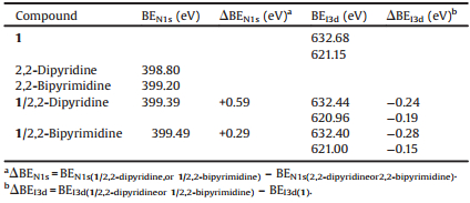
Naphthalene diimides (NDIs) are one of the most popular building blocks for constructing n-type OSCs for OFETs [11-13]. Gao and coworkers developed a series of symmetrically and unsymmetrically N-substituted core-expanded NDIs (NDI-DTYM2 derivatives) with fused sulfur heterocycles and end-capped electron-withdrawing groups [12a-d, 13], which could be synthesized by a mild and versatile one-pot synthesis [13], and exhibited high electron mobility in ambient conditions. Herein, we designed and synthesized an unsymmetrically N-substituted NDI-DTYM2 derivative (1) as an n-type OSC and also an XB donor that could form complementary XBs with 2, 2-dipyridine or 2, 2-bipyrimidine acceptor (Scheme 1). The supramolecular assembly of 1 by XBs was confirmed in some degree by thermogravimetric analysis (TGA), nuclear magnetic resonance (19F NMR, solid-state 13C NMR) and X-ray photoelectron spectroscopy (XPS). More importantly, the average electron mobilities of OFETs based on XB complexes 1/2, 2-dipyridine or 1/2, 2-bipyrimidine are higher than those of devices based on pure 1, demonstrating the important role of XB in improving device performance.

|
Download:
|
| Scheme 1. Molecular structures of compounds 1, 2, 2, 2-dipyridine, 2, 2-bipyrimidine, two XB complexes (1/2, 2-dipyridine and 1/2, 2-bipyrimidine). | |
The XB complexes 1/2, 2-dipyridine and 1/2, 2-bipyrimidine were prepared by mixing a 2:1 molar ratio of theXB-donor (1) and XB-acceptor (2, 2-dipyridine or 2, 2-bipyrimidine) in dichloro-methane (DCM), and then removed the solvent. The thin films of XB complexes were obtained through spin coating their respective DCM solution (5mg/mL, for each complex) onto octadecyltrichlorosilane (OTS)-treated SiO2/Si substrates. Gold source and drain contacts (50nm in thickness) were deposited by vacuum evaporation on the organic layer through a shadow mask, affording a bottom-gate top-contact (BGTC) device configuration. The channel length (L) and width (W) were 31 mm and 273 mm, respectively. Electrical measurements of OFET devices were carried out in air.
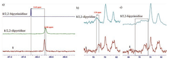
Compounds 1 and 2 were synthesized and characterized by 1H NMR, 13C NMR spectra and elemental analysis (see Supporting information for details). TGA, differential scanning calorimetry (DSC), UV-vis absorption spectra, and cyclic voltammetry (CV) were carried out to evaluate their thermal, optical, and electrochemical properties (see Supporting information for details). TGA showed that the thermolysis onset temperatures for 1 and 2 were both at about 345 ℃, (Figs. S1 and S4a in Supporting information), which indicated that 1 and 2 had good enough thermally stability. According to the DSC measurements from room temperature to 300℃, compounds 1 and 2 showed no apparent endothermic and exothermic peaks (Figs. S1b and S4b in Supporting information). UV-vis measurement was performed to estimate optical properties of 1 and 2 in solution, and their optical gaps were 1.97 eV and 2.00eV, respectively, estimated from the edges of their respective absorptions. As shown in Figs. S3 and S6 in Supporting information, compounds 1 and 2 both displayed two reversible reduction processes in DCM solution, with the first half-wave reductive potentials (Ered11/2) of 0.011eV and -0.039 eV, respectively (Table S1 in Supporting information). The LUMO energy levels of 1 and 2 were both at about -4.4 eV, which made them ideal n-type OSCs for OFETs.
OFETs based on compounds 1 and 2 were fabricated by spincoating their respective DCM solution (5 mg/mL) onto the OTS-treated SiO2/Si substrates with a BGTC device configuration. OFETs based on 1 (annealed at 120 ℃) showed an average electron mobility of 0.04 cm2 V-1 s-1, an average threshold voltage of 14.2 V, and a current on/off ratio of 104. When annealed at 80 ℃, thin-film device based on 2 gave an average mobility of 0.08 cm2 V-1 s-1, an average threshold voltage of7.6V, and a current on/off ratio of 104 (Fig. S7 in Supporting information). X-ray diffraction (XRD) and atomic force microscope (AFM) studies on thin films of 1 and 2 were showed in Figs. S8 and S9 in Supporting information, respectively. Thin films of 1 showed no diffraction peak even after high temperature thermal annealing, while those of 2 displayed a first-order diffraction peak (Fig. S9), suggesting better crystallinity of the films of 2 than that of 1, which might explain a superior FET performance of 2-based device relative to thin-film device of 1.
The formation of XBs in the complexes could be characterized by several techniques, involving Fourier transform infrared (FT-IR) and Raman spectroscopy (Raman), XPS, NMR and single crystal XRD [6, 7]. The thermal properties of the XB complexes could be investigated by DSC and TGA [14].To characterize the formation of XBs in the complexes 1/2, 2-dipyridine and 1/2, 2-bipyrimidine, TGA, XPS and NRM spectroscopy were adopted, in addition, we also performed the contrast test in this study using another NDI-DTYM2 derivative 2 (Scheme 1, 2 could not act as a XB donor and was used to form mixtures with 2, 2-dipyridine or 2, 2-bipyrimidine, respectively).
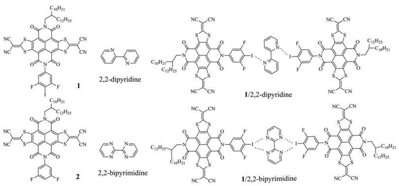
TGA measurements on 1, 2, 2-dipyridine, 2, 2-bipyrimidine, XB complexes 1/2, 2-dipyridine and 1/2, 2-bipyrimidine were carried out and showed in Fig. 1. The sublimation temperatures of 2, 2-dipyridine and 2, 2-bipyrimidine are 83 ℃ and 128 ℃, respectively. The onset decomposition temperatures of complexes 1/2, 2-dipyridine and 1/2, 2-bipyrimidine were 180℃ and 167 ℃, respectively. Therefore, the sublimation for both 2, 2-dipyridine and 2, 2-bipyrimidine in the complexes with 1 became more difficult, indicating the strong interactions between 1 and 2, 2-dipyridine or 2, 2-bipyrimidine [15]. Moreover, the temperatures for the complete sublimation of 2, 2-dipyridine and 2, 2-bipyrimidine from their respective complexes with 1 were 225 and 210 ℃, respectively. The above results suggested that an thermal annealing temperature ≤ 120 ℃ could not damage the XBs in the complexes 1/2, 2-dipyridine and 1/2, 2-bipyrimidine.

|
Download:
|
| Fig. 1. TGA plots of compounds 1, 2, 2-dipyridine and complex 1/2, 2-dipyridine (a), and the ones of compounds 1, 2, 2-bipyrimidine and complex 1/2, 2-bipyrimidine (b). | |
XPS is a spectroscopic approach to investigate intermolecular interactions (such as ionic and H bonding interactions) through the change of binding energy (BE) [8, 14-16]. The XPS spectra of spin-coated films on the clean silicon substrates were studied. As shown in Fig. S10 in Supporting information, the binding energies of the I3d doublet and N1s forXB complexes (1/2, 2-dipyridine and 1/2, 2-bipyrimidine) and XB donor (1) were studied and gathered in Table 1.
|
|
Table 1 BEN1s and BEI3d of compound 1, 2, 2-dipyridine, 2, 2-bipyrimidine, 1/2, 2-dipyridine and 1/2, 2-bipyrimidine. |
In two complexes, one shift to lower energy for the I3d doublet signal is observed (ΔBEI3d: from -0.15eV to -0.28eV), and the other shift to higher energy for N1s (ΔBEN1s: from 0.29eV to 0.59 eV) relative to the BEI3d values of the 1 and the BEN1s values of 2, 2-dipyridine or 2, 2-bipyrimidine, respectively. According to the literature [16b], when the iodine and nitrogen atoms were involved in XB, the electron density of the iodine atom would increase while that of the nitrogen atom would decrease, resulting in downshift of BEI3d and upshift of BEN1s. These changes ofbinding energies of I3d and N 1s in the complexes of 1/2, 2-dipyridine and 1/2, 2-bipyrimidine relative to the corresponding pure samples demonstrated that N…I-Rf halogen-bonding interactions existed between compound 1 and 2, 2-dipyridine or 2, 2-bipyrimidine in the thin films [14].
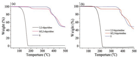
NMRs are useful analytical techniques for studying noncovalent interactions in solution and solid state, of which 19F NMR is a simple, sensitive and convenient tool to evaluate the interactions involving in electron donor-acceptor in the liquid phase [17]. To further characterize the existence of the halogenbonding interactions in the complexes, 19F NMR spectra of 1/2, 2-bipyrimidine in CDCl3 showed a high field shift of about 0.60ppm for the signal of Ar-F relative to that of compound 1 (Fig. 2a). While 19F NMR signal of 1/2, 2-dipyridine had no obvious change, which is probably because the C-I -N halogen bonds of 1/2, 2-dipyridine are weaker than the bifurcated C-I…NN halogen bonds of 1/2, 2-dipyrimidine (Scheme 1) [18].
Solid-state NMR spectroscopy can provide valuable information for subsequent characterization of systems where single crystals and long-range-order crystalline are absent [19]. CP-MAS (Cross Polarization, Magic Angle Spinning) 13C NMR experiments on compound 1, complexes of 1/2, 2-dipyridine and 1/2, 2-bipyrimi-dine revealed that the resonances of the carbon atom bonded with iodine atom undergo change from 1 to its complexes. As shown in Fig. 2b, the peak of 13C-I of 1/2, 2-dipyridine shifted about 1.56 ppm to downfield compared to that of compound 1 (from 74.15 to 75.71 ppm). For 1/2, 2-bipyrimidine, the signal of 13C-I showed wide and weak peaks due to there were fewer hydrogen atoms around C-I…NN than those around C-I…N of 1/2, 2-dipyridine (Fig. 2c), and thus there was not enough magnetization vector of1H was transferred to 13C bonded with iodine atom, leading to the weak and wide peaks [15]. The NMR data indicated the formation of XBs between compound 1 and 2, 2-dipridine or 2, 2-bipyrimidine.

|
Download:
|
| Fig. 2. a) 19FNMR spectra of 1, 1/2, 2-dipyridine and 1/2, 2-bipyrimidine in the CDCI3; b) Solid-state 13C NMR spectra of 1 and 1/2, 2-dipyridine; c) Solid-state 13C NMR spectra of 1 and 1/2, 2-bipyrimidine. | |
To explore the impact of XBs on FET performance of compound 1, OFETs based on 1, 1/2, 2-dipyridine and 1/2, 2 bipyrimidine were fabricated by spin-coating methods, affording the bottom-gate top-contact (BGTC) device configuration. Compound 2 was unable to form XBs, and was used to compare with 1. OFET devices based on 2, 2/2, 2-dipyridine and 2/2, 2-bipyrimidine mixtures both with a 2:1 molar ratio were fabricated and tested as contrasts. All the devices exhibited stable electron transport in air, with well-defined linear and saturation regimes (Fig. 3 and Fig. S7 in Supporting information).

|
Download:
|
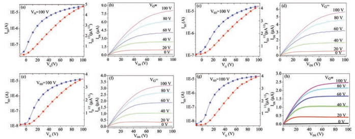
| Fig. 3. Transfer and output characteristics of as-spun OFETs based on active layers of 1/2, 2-dipyridine (a, b), 1/2, 2-bipyrimidine (c, d), 2/2, 2-dipyridine (e, f) and 2/2, 2-bipyrimidine (g, h), respectively. | |
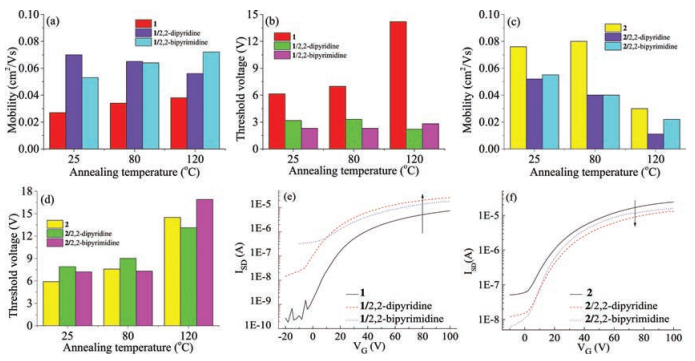
OFETs based on 1/2, 2-dipyridine and 1/2, 2-bipyrimidine displayed better device performance relative to that of devices based on 1, while OFETs based on the mixtures of compound 2 with 2, 2-dipyridine or 2, 2-bipyrimidine exhibited even worse device performance than that of devices based on 2. The measured average electrical parameters of all OFET devices are summarized in Tables S2 and S3 in Supporting information. The electron mobilities of OFET devices based on 1/2, 2-dipyridine or 1/2, 2-bipyrimidine were higher than those of devices based on 1 (Fig. 4a), with a two-fold or even higher increase for electron mobility from 0.027 cm2 V-1 s-1 to 0.070 cm2 V-1 s-1 and 0.053cm2V-1s-1, for devices based on 1, 1/2, 2-dipyridine and 1/ 2, 2-bipyrimidine, respectively (Table S2). The transfer characteristics of as-spun OFETs based on 1, 1/2, 2-dipyridine and 1/2, 2-bipyrimidine (Fig. 4e), demonstrated an obvious electron mobility increase when 1 was mixed with 2, 2-dipyridine or 2, 2-bipyrimidine. Meanwhile, the threshold voltages of OFETs based on 1/2, 2-dipyridine or 1/2, 2-bipyrimidine decreased in comparison with that of corresponding devices based on 1 (Table S2 in Supporting information, Fig. 4b). On the contrary, the electron mobilities of OFET based on 2/2, 2-dipyridine or 2/2, 2-bipyrimidine were all lower than those of device based on 2, with the optimized average electron mobilities decreased from 0.08cm2V-1 s-1 (for 2-based devices annealed at 80 ℃) to 0.04 cm2 V-1 s-1 (for 2/2, 2-dipyridine or 2/2, 2-bipyrimidine based devices annealed at 80 ℃) (Table S3 in Supporting information, Figs. 4c and f). As shown in Fig. 4d, the threshold voltages of OFETs based on 2/2, 2-dipyridine or 2/2, 2-bipyrimidine slightly increased relative to those of device based on 2. The results demonstrate that devices based on XB complexes of 1 show superior mobilities in general relative to those of 1-based OFETs owing to the XB interactions in controlling molecular packing of 1 and thus favour charge transport in the thin-film, while OFETs based on 2/2, 2-dipyridine or 2/2, 2-bipyrimidine exhibit worse performance compared to that of devices based on 2 due to the doped impurity of active layer of 2 by 2, 2-dipyridine or 2.2-bipyrimidine.

|
Download:
|
| Fig. 4. The column images for electron mobility of OFETs based on active layers of compound 1 (red), 1/2, 2-dipyridine (purple) and 1/2, 2-bipyrimidine (blue) (a), and of compound 2 (yellow), 2/2, 2-dipyridine (purple) and 2/2, 2-bipyrimidine (blue) (c) as a function of annealing temperature; The column images for the threshold voltage (absolute value) of OFETs based on active layers of compound 1 (red), 1/2, 2-dipyridine (green) and 1/2, 2-bipyrimidine (prunosus) (b), and of compound 2 (yellow), 2/2, 2-dipyridine (green) and 2/2, 2-bipyrimidine (prunosus) (d) as a function of annealing temperature; transfer characteristics of OFETs based on active layers of: compound 1, 1/ 2, 2-dipyridine and 1/2, 2-bipyrimidine (e), and of compound 2, 2/2, 2-dipyridine and 2/2, 2-bipyrimidine (f), respectively. | |
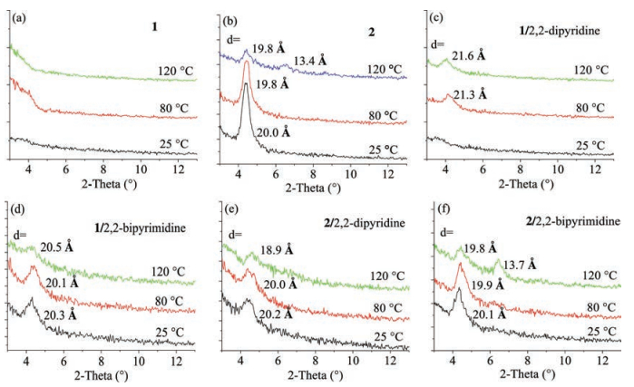
XRD measurements on thin films of compounds 1, 2, 1/2, 2-dipyridine, 1/2, 2-bipyrimidine, 2/2, 2-dipyridine and 2/2, 2-bipyr-imidine were performed to investigate their crystallinity. As shown in Fig. 5a, XRD patterns of thin films of 1 did not show any obvious Bragg reflections even at high annealing temperature, implying a less-ordered microstructure. XRD images of films of 2 all showed first order peaks with similar d-spacing distances at different annealing temperature (Fig. 5b). As shown in Figs. 5c and d, the thermal annealed films of 1/2, 2-dipyridine exhibited obvious peaks at 2θ = 4.10° with d-spacing distances of about 2.1 nm. In the case of the thin films of 1/2, 2-bipyrimidine, the XRD patterns showed sharp Bragg peaks for as-spun and thermal annealed thin films, with the d-spacing values of about 2.0nm. The AFM images of thin films of XB complexes also possessed larger domain size relative to those of 1 (Fig. S11 in Supporting information). A slightly different for d-spacing between 1/2, 2-dipyridine and 1/2, 2-bipyrimidine might suggest the different molecular arrangement in thin films and thus their different device performance. As shown in Figs. 5b, e and f, thin films of 2/2, 2-dipyridine and 2/2, 2-bipyrimidine both showed weaker Bragg reflections relative to those of 2 with d-spacing distances of 1.9-2.0nm, indicating that the mixtures of 2 did not form better ordered microstructure in solid-state than that of 2. In addition, the films of 2/2, 2-dipyridine showed a similar morphology with those of 2, yet the AFM images of the films of 2/2, 2-bipyrimidine exhibited some defects (Fig. S12 in Supporting information). Therefore, mixing 2, 2-dipyridine or 2.2-bipyrimidine with 1 can efficiently increase the crystallinity of the active layer and obtain better device performance than that of pure 1, due to the formation of XBs between 1 and 2, 2-pyridine or 2.2-bipyrimidine. While the films of 2/2, 2-dipyridine and 2/2, 2-bipyrimidine showed inferior crystallinity relative to that of 2, because of doped impurity (2, 2-dipyridine or 2, 2-biprimidine) in active layer of 2.

|
Download:
|
| Fig. 5. XRD patterns of spin-coated thin films of compound 1 (a); compound 2 (b); 1/2, 2-dipyridine (c); 1/2, 2-bipyrimidine (d); 2/2, 2-dipyridine (e); and 2/2, 2-bipyrimidine (f) after thermal annealing at different temperatures. | |
In this study, we carried out some experimental studies involving TGA, XPS, 19F NMR, solid-state 13C NMR, and preliminarily confirmed the formation of C-I-…N XB between compound 1 and 2, 2-dipyridine or 2, 2-bipyrimidine, and successfully utilized the blended active layers of 1 with 2, 2-dipyridine or 2, 2-bipyrimidine in OFETs, and the XBs in the blended thin films obviously promoted OFET performance with much increased electron mobility and slightly decreased threshold voltage. This improved device performance could be attributed to the improved molecular stack-ordering and thin-film crystallinity through XBs in the active layers of 1. On the contrary, OFET performance of devices based on 2/2, 2-dipyridine or 2/2, 2-bipyrimidine were lower than that of devices based on pure 2 due to the doped impurity of active layer of 2 by 2, 2-dipyridine or 2, 2-bipyrimidine. The results show that molecular design in consideration of the formation of XBs is a promising strategy to obtain high performance OSCs for OFETs, and may also pave a way for structural control of π-conjugated molecules in a variety of organic electronic devices.
AcknowledgmentsThis study was supported financially by the National Natural Science Foundation of China (Nos. 21502218 and 21522209) and the "Strategic Priority Research Program"(No. XDB12010100).
Appendix A. Supplementary dataSupplementary data associated with this article can be found, in the online version, at http://dx.doi.org/10.1016/j.cclet.2017.06.008.
| [1] |
(a) A. R. Murphy, J. M. J. Frechet, Chem. Rev. 107(2007) 1066-1096; (b) C. Wang, H. Dong, W. Hu, et al., Chem. Rev. 112(2012) 2208-2267. |
| [2] |
(a) R. W. Friend, R. W. Gymer, A. B. Holmes, et al., Nature 397(1999) 121-128; (b) C. L. Chochos, N. Tagmatarchis, V. G. Gregoriou, RSC Adv. 3(2013) 7160-7181; (c) L. Lu, T. Zheng, Q. Wu, et al., Chem. Rev 115(2015) 12666-12731; (d) Z. Y. Luo, Z. Y. Lu, Y. Huang, Chin. Chem. Lett. 27(2016) 1223-1230; (e) H. W. Luo, Z. T. Liu, Chin. Chem. Lett. 27(2016) 1283-1292. |
| [3] |
H.T. Black, D.F. Perepichka, Angew. Chem. Int. Ed. 53 (2014) 2138-2142. DOI:10.1002/anie.201310902 |
| [4] |
F.J.M. Hoeben, P. Jonkheijm, E.W. Meijer, et al., Chem. Rev. 105 (2005) 1491-1546. DOI:10.1021/cr030070z |
| [5] |
(a) M. Chang, D. Choi, B. Fu, et al., ACS Nano 7(2013) 5402-5413; (b) J. Lee, J. H. Park, Y. T. Lee, et al., ACS Appl. Mater. Interfaces 6(2014) 4965-4973; (c) Y. Lin, Q. Wei, G. Qian, et al., Macromolecules 45(2012) 8665-8673; (d) K. H. Lam, T. R. B. Foong, Z. E. Ooi, et al., Interfaces 5(2013) 13265-13274; (e) F. Wang, X. Zhang, L. Wang, et al., ACS Appl. Mater. Interfaces 6(2014) 15098-15104. |
| [6] |
G.R. Desiraju, P.S. Ho, L. Kloo, et al., Pure Appl. Chem. 85 (2013) 1711-1713. DOI:10.1351/PAC-REC-12-05-10 |
| [7] |
(a) L. C. Gilday, S. W. Robinson, T. A. Barendt, et al., Chem. Rev. 115(2015) 7118-7195; (b) G. Cavallo, P. Metrangolo, R. Milani, et al., Chem. Rev. 116(2016) 2478-2601. |
| [8] |
F. Wang, N. Ma, Q. Chen, et al., Langmuir 23 (2007) 9540-9542. DOI:10.1021/la701969q |
| [9] |
(a) H. L. Yip, H. Ma, A. K. Y. Jen, et al., J. Am. Chem. Soc. 128(2006) 5672-5679; (b) P. Jonkheijm, N. Stutzmann, Z. Chen, et al., J. Am. Chem. Soc. 128(2006) 9535-9540; (c) M. Gsänger, J. H. Oh, M. Könemann, et al., Angew. Chem. Int. Ed. 49(2010) 740-743; (d) M. Bonini, L. Zalewski, E. Orgiu, et al., J. Phys. Chem. C 115(2011) 9753-9759. |
| [10] |
(a) Y. Kumar, S. Kumar, S. K. Keshri, et al., Org. Lett. 18(2016) 472-475; (b) A. Abate, M. Saliba, D. J. Hollman, et al., Nano Lett. 14(2014) 3247-3254. |
| [11] |
M.A. Kobaisi, S.V. Bhosale, K. Latham, et al., Chem. Rev. 116 (2016) 11685-11796. DOI:10.1021/acs.chemrev.6b00160 |
| [12] |
(a) X. Gao, C. Di, Y. Hu, et al., J. Am. Chem. Soc. 132(2010) 3697-3699; (b) X. Hu, X. Gao, C. Di, et al., Chem. Mater. 23(2011) 1204-1215; (c) F. Zhang, Y. Hu, T. Schuettfort, et al., J. Am. Chem. Soc. 135(2013) 2338-2349; (d) X. Gao, Y. Hu, J. Mater. Chem. C 2(2014) 3099-3117; (e) D. Lu, X. C. Yang, B. Leng, et al., Chin. Chem. Lett. 27(2016) 1022-1026. |
| [13] |
Y. Hu, Y. Qin, X. Gao, et al., Org. Lett. 14 (2012) 292-295. DOI:10.1021/ol203059r |
| [14] |
L. Gonzalez, N. Gimeno, R.M. Tejedor, et al., Chem. Mater. 25 (2013) 4503-4510. DOI:10.1021/cm401849f |
| [15] |
R. Bertani, P. Metrangolo, A. Moiana, et al., Adv. Mater. 14 (2002) 1197-1201. DOI:10.1002/1521-4095(20020903)14:17<1197::AID-ADMA1197>3.0.CO;2-V |
| [16] |
(a) X. Zhou, S. H. Goh, S. Y. Lee, et al., Appl. Surf. Sci. 119(1997) 60-66; (b) J. Xu, X. Liu, J. K. P. Ng, et al., J. Mater. Chem. 16(2006) 3540-3545. |
| [17] |
(a) M. T. Messina, P. Metrangolo, W. Panzeri, et al., Tetrahedron Lett. 39(1998) 9069-9072; (b)M. T. Messina, P. Metrangolo, W. Panzeri, et al., Tetrahedron 57(2001)8543-8550; (c) M. T. Messina, P. Metrangolo, W. Navarrini, et al., J. Mol. Struct. 524(2000) 87-94. |
| [18] |
B. Ji, W. Wang, D. Deng, et al., Cryst. Growth Des. 11 (2011) 3622-3628. DOI:10.1021/cg200603z |
| [19] |
(a) K. Bouchmella, S. G. Dutremez, B. Alonso, et al., Cryst. Growth Des. 8(2008) 3941-3950; (b) D. L. Bryce, J. Viger-Gravel, Top. Curr. Chem. 358(2015) 183-203. |