 2013, Vol. 1
The article information
- Bin-Shi Xu
- Carbon nanotubes for electronics manufacturing and packaging:from growth to integration
- Advances in Manufacturing, 2013, 1(1): 13-27
- http://dx.doi.org/10.1007/s40436-013-0007-4
-
Article history
- Received: 2012-03-10
- Accepted: 2012-06-25
- Published online: 2013-03-13


Ever since the electronic products shifted from vacuum tubes to transistors and integrated circuits (ICs),manufacturing and packaging technology is becoming increasingly important. Besides the size and cost consideration, manufacturing and packaging technology,to a great extent, also determines the performance and lifetime of a microsystem. Manufacturing and packaging technology bridges different parts in a microsystem to realize desired functions and meanwhile provide mechanical and chemical protection, to make the microsystem work as a whole.
While it becomes increasingly difficult and expensive to further shrink the size of transistors in ICs,the future miniaturization of electronics to keep the Moore’s Law is expected to be mainly driven by the advances of the manufacturing and packaging technologies,which aim at increasing the density of integration at a system level. One of the most important trends in the technology development during recent years is the integration in a three-dimensional (3D) manner. The utilization of the vertical dimension is expected to dramatically promote the integration density.
However,higher integration density will also cause a variety of problems in manufacturing processes,in long term reliability,and in thermal management. To meet these challenges,one key research area is the utilization of novel materials,especially the nano-structured materials. Among these materials,carbon nanotubes (CNTs) have attracted extensive interest due to their unique mechanical,thermal, and electrical properties.
The application of CNTs in the manufacturing and packaging field has at least three scenarios,i.e.,integrating CNTs into thermal interface materials (TIMs),applying CNTs for interconnection and using CNTs as cooling fins. It should be pointed out that electronics manufacturing is a highly multi-disciplinary field,involving so much scientific and engineering knowledge,that it is not possible to cover all the aspects of such a complex system. This paper reviews the use of CNTs for electronics manufacturing purposes with the focus on the growth method and integration technology. 2 Growth methods of CNTs
The physical properties of CNTs are very much dependent on how they are grown. Commonly there are three mostly used methods to grow CNTs,namely arc discharge,laser ablation and chemical vapor deposition (CVD). Each method requires carbon feedstock and a certain temperature condition. On one hand,the arc discharge and laser ablation methods produce CNTs at higher temperatures which lead to better controlled qualities and in large quantities in their nature. On the other hand,although giving CNTs of relatively lower quality and quantity,CVD grown CNTs have the flexibility of defining specific grown regions by patterning the catalyst fiµms which is very much desired in many electronics applications. The following sections will overview these methods briefly. 2.1 Arc discharge
This method utilizes two graphite electrodes facing each other in a sub-atmosphere environment [1]. A current of tens of amperes is applied to generate electrical discharge which leads to a local high temperature of around 2,000 °C. The graphite will sublimate at the high temperature and carbon atoms are ejected from the electrode to form plasma. As these carbon atoms move towards colder area,CNTs are synthesized. Most CNTs synthesized in this way are multi-walled. Introducing transition metals such as iron (Fe),cobalt (Co),nickel (Ni) and yttrium (Y) into the graphite electrode,single-walled carbon nanotubes (SWNTs) will be dominant in the product [2].
The synthesis is commonly processed in an inert environment such as helium and argon to prevent carbon feedstock and CNTs from oxidation. Nevertheless,synthesis in other environments has also been reported. For instance,Zhao et al. [3] found that the CNT synthesis by arc discharge method in hydrogen atmosphere generated less carbon smoke than that in methane and helium. In addition,the quality of the CNTs is also higher. Shimotani et al. [4] found that the synthesis in organic gases such as ethanol,acetone and hexane produced more multi-walled carbon nanotubes (MWNTs) than the synthesis in helium.
The CNTs grown by arc discharge method show few structural defects but contain a lot of impurities which are mainly carbon nano-particles [5]. This method also has poor control on the alignment of synthesized CNTs which is required in many electronics and microsystems applications. 2.2 Laser ablation
Laser ablationmethod is firstly applied to synthesizeCNTs by Smalley’s group in 1995 [6]. The setup configuration is very similar to that in arc discharge method. The difference is that the energy used to vaporize graphite is provided by laser other than arc discharge. The CNT synthesis process is also similar to the one in arc discharge method,with vaporized carbon species cooled down to form CNTs. The temperature during the synthesis is around 1,200 °C. Pure graphite electrodes are favored for MWNT syntheses whereas catalysts (such as Fe, Co,Ni,Y,etc.) mixed graphite electrodes are preferable to SWNT synthesis [7]. In contrast to the arc discharge method, laser ablation synthesizes CNTs with higher purity [8]. 2.3 Chemical vapor deposition
CVD is a catalytic process to grow CNTs. CVD method possesses advantages such as easily defined pattern,low impurity level,controllable morphology,large tube length, easy to scale up for industrial production,etc.,thus, attracting more interests than the other methods.
The catalyst is normally a metal,mostly a transition metal such as Fe,Ni,Co,or a metal alloy. There are two major ways to provide the catalyst for theCVDprocess. One method is to deliver the catalyst particles through the gas flow,namely floating catalyst [9] or fluidized bed catalyst method [10]. A more widely used approach is called supported catalyst method. The catalyst layer is deposited onto the substrate by physical vapor deposition processes prior to the CNT synthesis. A thin barrier layer,normally composed of several nanometers of oxides or nitrides,is usually deposited in between the catalyst and the underlying silicon,or metal substrate. The purpose of the barrier layer is to prevent the catalyst from diffusing into the substrate during the high temperature growth. A great advantage of this method is that by standard lithography process the patterns of the catalyst fiµm can be easily defined,naturally leading to any desired patterns of the synthesized CNT fiµms which are necessary for many applications. CNTs synthesized in this way are normally well aligned,vertical to the substrate. The deposited catalyst layer is often annealed first to form discrete nano-sized particles,which later catalyze the CNT synthesis. During the CVD of CNTs,carbon is usually provided through the flow of a hydrocarbon gas,such as C2H2 or CH4. The mechanism of catalytic CNT synthesis is a central topic of CNT research and still not fully understood. It has been widely accepted that it involves decomposition of hydrocarbon molecules on the surface of the metal particles,dissolution and diffusion of the carbon atoms in the particles, and precipitation of the carbon atoms on the surface to form nanotubes. Thus the diameters of the nanotubes are largely determined by the sizes of the metal particles,which can be varied by controlling the thickness of the deposited catalyst fiµm. From a macroscopic perspective,the CNTs "grow" from the seeding catalyst particles. This is probably why growth is the common term of catalytic synthesis of CNTs. CNT growth can be either a base growth,in which the metal particles stay on the substrate,or a tip growth,where the particles are lifted and stay at the tips of the CNTs. Figure 1 shows the model of a commercially available CNT CVD growth system provided by AIXTRON.
 |
| Fig. 1 Commercially available CNT CVD system,Black Magic II, by AIXTRON |
Depending on the form of supplying energy to the reaction, CVDofCNTfalls into twomain categories,i.e.,thermalCVD (TCVD) and plasma-enhancedCVD(PECVD). The theory of how plasma affects the CVD process of CNTs is still lacking. But it is a widely adopted approach to use the Ni catalyst and plasma to obtain thick (diameter[50 nm) and short (length <2 µm) fiber-like nanotubes,while Fe catalyst is generally used in TCVD processes for the generation of thinner (diameter<40 nm) and longer (length>10 µm) single and multi-walled nanotubes. There are a variety of reactor designs for both types. For example,a PECVD system for CNT growth may be equipped with direct-current (DC),hot-filament direct-current (HF-DC),or microwave plasma source, etc. [11] The length of the grown CNTs can be controlled by adjusting the growth parameters such as gas flow,temperature, and growth time. The resulting tube length ranges froma few microns up to several millimeters [12, 13].
Figure 2 is the illustration of a typical TCVD process and the scanning electron microscopy (SEM) picture of its resulting CNT bundles. Figure 3 is the SEM picture of the typical growth results of PECVD using Ni as catalyst. Comparing these two figures,it can be easily found that the Fe catalyzed TCVD generates very different growth results from Ni catalyzed PECVD growth.
 |
| Fig. 2 a Illustration of the TCVD CNT growth technology and b SEM image of thermally grown CNT forest structures using Fe as catalyst with Al2O3 underlayer (Inset side view zoom-in of the CNT walls) |
 |
| Fig. 3 a SEM picture of the PECVD-grown CNTs using a thin fiµm of Ni as catalyst and b SEM picture of the PECVD-grown CNTs using pre-patterned Ni catalyst lines as catalyst |
As the growth condition of CNTs usually involves high temperature (>700 °C),long time heating (>5 min),and corrosive environment (H2/NH3 and plasma),it is very difficult to directly grow CNTs on the target surface for any electronics application. In addition,as-grown CNTs usually have a low volume fraction,which means that the individual CNTs are spaced with huge air gaps. Therefore,it is highly necessary to figure out a way to take the as-grown CNTs off the original growth substrate and put it onto the target surface in a condensed manner. These processes are generally referred to as transfer and densification for the post processing of CNTs. In the following sections,we will give a brief summary of the available post processing methodologies developed for CNTs. 3.1 Transfer of CNTs
In order to integrate CNTs into microsystems,their compatibility with current materials,devices,and manufacturing processes is a critical concern. One major problem with growing CNTs by CVD is the high growth temperature, which exceeds the tolerance of many materials and devices, for example the CMOS circuitries. While significant progresses have been made in low temperature CNT growth, there is always a dilemma of trading off CNT quality for lower growth temperature. To solve this problem,one approach is to grow CNTs at a high temperature and then to transfer them to the target substrate at a low temperature using a transfer medium,e.g.,solders or conductive adhesives (CAs). This transfer strategy also provides a solution to the problem of CNTs’ selective growth on different underlayer materials. Transferring CNTs after growth brings the freedom to choose any substrate and growth parameters that generate CNTs of high quality. Furthermore,this transfer strategy makes it possible to apply post-growth treatment such as doping and high temperature annealing,before CNTs are assembled to devices not allowing such processes.
Table 1 summarizes the previous work on low temperature transfer of CNT structures. This summary is limited to those work in which the CNTs are vertically aligned both before and after the transfer process. It should be noted that there are many other papers on transferring randomly or horizontally aligned CNTs for applications such as transistors or interconnects as well.
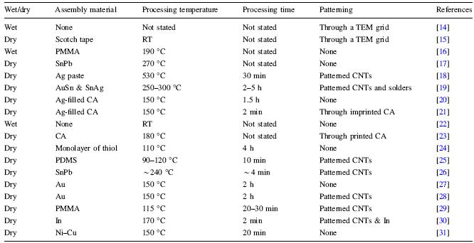
Regarding the transfer of CNTs,this process falls into two major categories. One category,denoted "wet" method herein,involves a lift-off step to separate the CNTs and the growth substrate by etching away the barrier layer,commonly done in hydrofluoride (HF). After that,the stand-alone CNT fiµms are placed onto the target substrate. Because this method requires handling of entire stand-alone fiµms,it is difficult to employ any fine patterning or alignment during the transfer. In addition the liquids involved during the transfer process are likely to distort and change the metrology of the CNTs which makes the structures more difficult to handle. Moreover,this approach normally does not apply an assembly material between the CNTs and the target,making the adhesion between them quite weak. Therefore the applicability of this wet method is very limited.
A more widely studied and implemented route is to use an assembly material to transfer CNTs,eliminating the wet processing step. These are marked as "dry" methods in Table 1. A variety of materials has been used for the transfer purpose,including pure polymeric materials,conductive adhesives,and metals,etc. If the electrical conduction from the CNTs to the substrate is needed,only conductive materials can be used. The processing temperature of these dry transfer methods varies from room temperature to higher than 500 °C. The processing time ranges from a few minutes to a few hours. The quality of the dry-transferred CNTs are generally good compared with those done by the wet methods, as the distortions during the processing can be precisely controlled on the equipment used. An example of transferred CNT bundles using indium as assembly material is shown in Fig. 4. By carefully controlling the pressure and spacing of substrates,the distortion of CNTs can be minimized.
 |
| Fig. 4 CNT bundles transferred onto indium-coated target substrate (The CNT bundles are pre-densified using vapor densification method [32]) |
VA-CNT structures made by CVD are a highly porous material with a typical porosity above 90 % [33],i.e.,less than 10 % of the total volume of a VA-CNT forest is occupied by CNTs. The high porosity of VA-CNT structures is an important advantage in certain cases,such as in sensing applications where a large surface area is desired. It is however a drawback in some other electronics applications which require a high volume fraction of CNTs. For example,the high porosity makes VA-CNT structures ineffective in thermal and electrical transport,and also deteriorates their mechanical strength. Therefore it is essential to create VA-CNT structures in which the nanotubes are closely packed.
Attempts were made to optimize the catalyst to allow for direct growth of dense CNT forests [34, 35, 36]. However their density was still far from that of closely packed ones. An alternative approach is to densify the VA-CNT forests after their growth,as shown in Fig. 5. Futaba et al. [37] demonstrated that porous CNT forests could be densified to closely packed CNT solids by capillary force from a solvent in which they were immersed. The interactions between CNTs and liquids were actually studied earlier to generate self-assembly in CNT fiµms [35, 36, 38, 39]. This immersion-based wet densification method was applied to make CNT-polymer composites [40] and to improve the electrical performance of CNT interconnects [41, 42]. This method was later modified in diverse ways to create dualporosity CNT structures [34]. One of the modifications reported in Ref. [34] was to expose the CNTs to a solvent vapor instead of direct immersion. The vapor densification method has been further investigated to create diverse CNT structures [43].
 |
| Fig. 5 a,b Schematic of densifying CNTs using the solvent vapor method; SEM picture of c original CNT bundles and CNT bundles densified for d 20 s,e 30 s,f 40 s,g 50 s,and h 60 s (adopted from Ref [32]) |
Besides,VA-CNT structures can also be densified by dry methods in which external forces were applied to press the CNTs together [44, 45]. This approach is however not capable of densifying microscale patterned VA-CNT structures to full dense structures. 4 Integration of CNTs into microsystems
This section tries to connect the as-discussed processing technology with practical applications which is going to explore one or several excellent features of the CNTs and put them into working systems. The interconnect applications are mostly concerned with the electrical,thermal and mechanical properties of the CNTs. The TIM and cooling fins application,on the other hand,focuses more on the thermal capabilities of the CNTs. The aforementioned growth,densification,and transfer processes are all utilizable in these three kinds of applications and are tuned to accommodate specific requirements application. 4.1 CNT-based interconnections
Some of the properties of CNTs,for example,their high current carrying capacity,low electromigration and Joule heating,high thermal conductivity,mechanical flexibility and low thermal expansion,are very attractive for interconnect application. Hence,CNTs have been proposed as promising candidate materials to build next generation interconnects in miniaturized electronics,as both on-chip and off-chip interconnects.
A series of modeling work on CNT interconnects has been done by Naeemi and Meindl [46, 47, 48]. A very simplified introduction to the basis of their work is given in this subsection.
The modeling of the capacitance and inductance components of CNT interconnects can be found in Ref. [49, 50]. A high frequency analysis of CNT interconnects has also been performed [51],in which one interesting conclusion is that the skin effect of CNT interconnects is significantly less severe than that of metal lines.
Based on the model described in the reference listed above, the resistances ofCNT off-chip interconnects,such as throughsilicon- vias (TSVs),can be estimated by straightforward calculations assuming some typical dimensions. AnMWNT with 30 nm outer diameter and 15 nm inner diameter,100 µm length,and 1 µmelectronmean free path,at room temperature has a conductance of 0.048 kΩ-1. This leads to an estimated resistance of 21 kΩ for such an MWNT if all its walls can be contacted. Note that here the electronmean free path is taken as 1 µm based on experimental observations such as in Ref. [52]. Therefore,if a loosely packed CNT forest can be densified into closely packed bundle,as illustrated in Fig. 6,the conductivity of such a structure can be greatly increased.
 |
| Fig. 6 Arrangement patterns of CNTs a loosely packed with roughly 93 % porosity and b closely packed with an inter-tube distance of around 0.34 nm (not drawn to scale) |
Based on the discussion above,the following requirements for CNT-based interconnects can be identified:
(i) High structural quality of CNTs. The structural quality of CNTs directly affects the performance of CNT-based interconnects. In general,the higher the growth temperature,the better the CNTs grow. The best quality CNTs available on the market are mostly fabricated using arc discharge and laser ablation methods,which input much more energy during the growth than the TCVD process. The quality of TCVD growth is an area requiring significant efforts.
(ii) Large fraction of metallic CNTs. It is important for applications requiring the use of SWNTs. This is however not amust ifMWNTs with large diameters are used as interconnects,because MWNTs are generally conductive due to their large number of walls.
(iii) Large volume fraction of CNTs in the structures. This requirement can be met by adopting the methods discussed in the previous densification sections. The problem of such densification methods is that they are not yet proved to be applicable in industrial manufacturing scale.
(iv) Good compatibility with existing materials,devices, and manufacturing processes. Contact of CNTs with other materials is another important subject. The contacts between CNTs and different metals have been made and compared [53, 54, 55],showing the possibility to achieve ohmic CNT-metal contacts with low resistances. Rapid thermal annealing has been used to decrease the contact resistance and to improve the contact’s long time stability [54, 56].
(v) Reasonable process time and manufacturing cost. As any practical technology,the time and cost of making CNT-based interconnects must be taken into account. No significant additional process time is expected because growth of CNTs is generally a quick and parallel process which normally lasts for a few minutes to 1 or 2 h. The subsequent processes are also standard manufacturing processes. Recent development of commercial CNT growth systems makes CNT growth very close to a standard and cost-effective manufacturing process. Figure 7 shows a typical fabrication process [57] flow of CNT based TSVs which is compatible with standard CMOS technology.
 |
| Fig. 7 a-hCMOScompatible process for fabricating CNT based TSVs and i the SEMpicture of the transferred and densified CNTs inside a via [57] |
Recent processes [21, 57, 58] in making CNT based interconnects have demonstrated the integration of CNTs into TSV and bump array structures. Figure 8 is sample results of using CNT bundles in interconnect bump applications and TSV interconnect applications. The processes used are compatible with current industrial manufacturing environment,although the resistivity of such CNT based interconnects (~10-5 Ωm) does not excel that of the metals. Processes such as transfer and densification have already been cooperated in order to achieve the compatibility issues. The next steps of the integration research should probably be focusing on how to decrease the resistivity of the CNTs so that they can compete with metals in general applications.
 |
| Fig. 8 a CNT interconnect bump in contact with Au surface (Inset zoom-in of the CNT-Au interface) and b CNT bundles interconnecting with CNT bundles in a TSV scenario (Inset zoom-in of the CNT- CNT interface) [58] |
The function of TIMs is to fill the micro-scale gaps between two contacting surfaces for an efficient thermal transport through this interface. In a component package, TIMs are typically applied between the die and the lid,also called integrated heat spreader (IHS),and also between the IHS and the cooling device. Beside the obvious significance in thermal transport,TIMs also play a critical role in maintaining the reliability of the component package by absorbing the thermomechanical strain [59, 60]. Therefore, both thermal and mechanical properties are important in selecting and developing TIMs.
The most widely used TIMs are polymeric composites filled with thermally conductive metallic or ceramic particles. Pure indium,a highly conductive and ductile metal, is also commonly used as TIM1 in high-performance applications [61, 62, 63].
Developing TIMs with better thermal and mechanical properties is one of the key measures to meet the increasingly difficult thermal management challenge. The high thermal conductivity of CNTs makes them a natural selection for developing or improving TIMs. The application of CNTs in TIMs falls into two major categories,as shown in Fig. 9 [64]. The first one is to add CNTs into polymer matrix as randomly oriented fillers. It was shown that a small filling ratio of CNTs (1 wt%) can significantly enhance the thermal conductivity of the composite (by 125 wt% at room temperature) [65]. Treatments such as magnetic field processing to introduce alignment of CNTs in the matrix can further improve the thermal transport [66]. Introducing a small amount of CNTs as extra filler into existing TIMs can also greatly promote their thermal conductivity by enhancing the heat transfer between the original filler [67]. The second approach is to use vertically aligned CNT fiµms directly,sometimes also infiltrated with a polymer,as TIMs,such as in Ref. [64, 68, 69]. The results in these references differ for a factor of 1-2 orders of magnitude,which may be due to the variations in the quality of CNT fiµms and measurement methods. In general, the measured thermal properties of most VA-CNT based TIMs are still poorer than those of typical metal systems even though the thermal conductivity of bulk VA-CNT fiµms can be quite high [70, 71].
 |
| Fig. 9 a Schematic of the idealized structure for highly anisotropic and efficient heat transport. Perfectly aligned,continuous nanotubes packed in high density completely eliminate the high thermal resistance at nanotube junctions; b schematic drawing of loose nanotube networks as found in bucky paper or chemically spun fibers comprised of short nanotubes. Thermal transport through the network in the direction of the arrow is limited by nanotube bundling,the presence of sidewall defects,and a large number of high thermal resistance nanotube junctions; c photograph of 6-mm-tall VA-CNT; d SEM photo of the top 70 µm of VA-CNT [64] |
It was found that the thermal contact resistances between the CNTs and the substrates dominate in the interfaces [55, 72, 73],thus their minimization is the key to develop efficient VA-CNT based TIMs. So far,there are three routes proposed to reduce the interfacial contact resistance. The first one is annealing or bonding of the CNTs to the metallic contacting surface [74, 75]. For example,Barako et al. [76] bonded as-grown CNTs onto solder and used it as TIM. Their measurements show that the solder bonded CNT-based TIM has a reduction of interfacial thermal resistance up to a factor of 30. The second route is creating functional group between CNTs and contacting surface,such as demonstrated by Lin et al. [77] whose results show that the thermal diffusivity of the CNT mediated interface is improved by one order of magnitude and the conductivity by aµmost two orders of magnitude after the functionalization. The third route is building up covalent bonding between CNTs in a matrix to reduce the phonon scattering on the thermal transportation path therefore reducing the total thermal resistance of the CNT based TIM. For instance,Fu et al. [78] demonstrated the synthesis of such interconnected CNT networks which could extend the excellent thermal performance of CNTs from one dimension to three dimensions using an electrospinning based template growth method. The fabrication method is illustrated in Fig. 10 and some experimental details are presented in Fig. 11.
 |
| Fig. 10 Synthesis flow chart of the covalently bonded 3D CNT networks a electrospinning of Ni(NO3)2 contained PVB nanofiber networks; b inter-connected electrospun Ni(NO3)2/PVB nanofibers in the network; c NiOx nanofiber network after the burning of PVB and decomposition of Ni(NO3)2 in O2; d pure Ni fiber network reduced from NiOx by H2; e graphitic layer growth on the inter-connected 3D Ni template; f chemical etching of Ni core in FeCl3 solution [78] |
 |
| Fig. 11 Fabrication and characterization of the covalently bonded CNT network a interconnected Ni(NO3)2 contained PVB nanofibers; b H2 reduced interconnected Ni fibers; cXRDpattern of theH2 reduced Ni fibers; d inter-connected Ni fibers with graphene layers grown on the cylindrical surfaces; e well crystallized graphene layers on the Ni fiber surface; f harvested CNT network after removing Ni template by chemical etching in FeCl3 solution; g covalently bonded,internally connected CNT multi-branched structure; h Raman spectrum of the harvested material [78] |
In the thermal management of microsystems,heat sinks or coolers consisting of arrays of cooling fins are often used to facilitate an efficient heat transfer from components to the ambient air by offering a large area of heat exchange surface. For applications where natural convection is not sufficient, fans are often attached onto the heat sinks to create more efficient forced convective cooling. Heat sinks used in both natural and forced convective cooling are mostly made of mechanically machined copper or aluminum.
CNTs in their forest form have also been used as cooling fins in both air and liquid cooling. CNTs applied in cooling systems as fin material was firstly introduced by Liu and his research group in 2004 [79, 80]. In Ref. [79, 80],a bare silicon chip was chosen as the substrate and after CVD synthesis,CNTs array was grown from the catalyst as cooling fins,as shown in Fig. 12. Finally,a lid was bonded to seal the CNTs and form the microchannels for cooling fluid. Cooling experiments were performed to test the CNT based microchannel coolers,and it was also compared with the cooler without CNTs array as cooling fins. Results showed that although the CNTs array decreased the flow rate of the fluid by 12 %,the CNT-based microchannel cooler showed much higher cooling capacity. With 23 % higher input power,the CNT-based microchannel cooler kept the transistor temperature 6 °C lower than the reference cooler (the cooler without CNT fins).
 |
| Fig. 12 Manufacturing procedure of CNT based microchannel cooler [76] |
Ekstrand et al. and Wang et al. [81, 82] further developed this module by simulation and experimental method respectively. Ekstrand et al. [81] simulated the heat transfer in the microchannel cooler by FEMLAB when water was used as coolant,then they compared the CNT-based cooler with the reference cooler. Results showed that thermal resistance of the microchannel cooler was reduced from 0.99 to 0.43 K/W when CNT fins were introduced, although pressure drop between inlet and outlet increased. On the other hand,due to the gap between the bottom of the lid and the top surface of the CNTs array,flow velocity of the water at the bottom of the channels was significantly reduced,which led to a great reduction of heat exchange between water and CNTs. Wang et al. [82] fabricated three kinds of microcoolers: CNT-based microchannel cooler, silicon-based microchannel cooler and microcooler without any fin. In their experiments,the power transferred from the heater to the cooler could not be measured precisely because there was an unknown portion of heat dissipated by natural convection. In addition,there was a considerable thermal resistance existing between the heat resistor and the cooler,which made an accurate calculation more difficult. However,because experimental conditions were well controlled,the research was meaningful to reveal the advantages and drawbacks of the CNT-based microchannel cooler. Wang et al’s experimental results indicated that the CNT-based microcooler was about 10-15 % better than silicon-based cooler. To cool the resistor to the same temperature (42 °C),CNT-based cooler needed a lower water flow rate (35.7 vs. 38.5 mL/min) under a higher power (2.13 vs. 1.95 W) loaded on heat resistor. Additionally,the bottom plate of the CNT-based cooler was much thicker than that of the silicon-based cooler because CNTs were grown on the plate while silicon-based cooler was made by etching into the plate,which meant the CNT-based cooler had a bigger thermal resistance between heat resistor and cooling fins.
Kordás et al. [83] grew MWNTs on Si/SiO2 templates from a xylene/ferrocene precursor by catalytic CVD deposited at 770 °C to form a thick CNT fiµm. Then they applied laser to etch the fiµm to get 10 9 10 fin array blocks. The structure they designed to test the CNT fins consisted of a thermometer flip chip mounted on a customized silicon substrate,and the array of the fin block itself being soldered onto the backside of the flip chip,as shown in Fig. 13. Their results presented in Fig. 14 showed that using natural convection,more 11 % power was observed to be dissipated from the chip that had the attached nanotube fin structures. While under forced N2 flow,the cooling performance with the fins was improved by 19 %. These results meant that applying the nanotube fin structure would allow the dissipation of about 30 and 100 W/cm2 more power at 100 °C from a hot chip for the cases of natural and forced convections,respectively. Because of the low density of CNTs,these results also meant an extra power dissipated per weight of added CNT structure can be as high as 1.1 and 3.7 kW/g for these two cases respectively. Korda´s et al. also compared the cooling performance of the CNT fins with copper fins,results showed that copper fins performed fairly equally to CNT fins. Computational fluid dynamics (CFD) simulation showed the heat transfer coefficient varied from 20 to 500 Wm-2 K-1 depending on the local flow rate,which agreed with published values very well.
 |
| Fig. 13 Phases of substrate/flip-chip/CNT-cooler assembling a positioning; b soldering the flip chip on the Cu landing pads of the substrate (this structure also served as a reference); c solder paste dispensing CNT array positioning; d soldering on the Cu coated backside of the chip; e field emission scanning electron microscopy image of an assembled structure (scale bar 500 µm) [83] |
 |
| Fig. 14 a Chip temperatures measured for chip-on-substrate (red plots) and for the corresponding CNT 10 × 10 fin array-on-chip-on-substrate assemblies (blue plots) under various heating powers and N2 flow rates,b results of a comparative experiment in which a finned copper cooler (10 × 10 array) was used [83] |
Zhong et al. [84, 85] carried out CFD simulation for a series of CNT microfin cooling architectures based on both one and two-dimensional (2D) fin array models. They considered the influence of microfin structures,fluid speed, heating powers and effective thermal conductivity on cooling effects,and they also compared the simulation with experiment results. The 2D CFD simulation indicated that the heat transfer capability of coolers was considerably dependent on the number of fin rows and the cooling capability of 2D CNT fin array was more efficient than that of 1D one. Simulation also showed that the fluid speed was the key factor of heat transfer,and the heat generated by the chip was removed mainly by liquid mass flowing in the channels of micro-fin architectures. The pressure drop between the inlet and outlet of the cooling device was an important factor limiting the fluid speed,and the excessive pressure drop may destroy the CNT fin structures. Maximum temperatures in fin arrays were dependent linearly on the chip heating power,and the linear relationship was corresponding to a constant thermal resistance of cooling system. Finally,they found the effective transverse thermal conductivity of CNT fins was also a crucial factor for cooling efficiency of the microfin structures,but they needed further experiments for verification.
Hu et al. [86] studied the air flowthroughCNT arrays using molecular dynamics simulations,the model is shown in Fig. 15. They found that for 1.4 nm diameter tubes separated by 25 nm,the air flow can be well described by the free molecular flow theory. They estimated for such array that the pressure gradient was about 10.1325 kPa/µm at 101.325 kPa air pressure and 5 m/s flow velocity,which indicated that the flowing air can only pass through an array of no more than about 400CNTs in series.They also gave suggestion forCNTs array design for thermal energy exchangewith air,as shown in Fig. 16. Jang and Choi investigated the cooling performance of a microchannel heat sink with nanofluids numerically [87]. The results showed that cooling performance of the microchannel heat sink was enhanced by about 10 % when nanofluids containing diamond (1 vol %,2 nm) was used. They thought nanofluids reduced both the thermal resistance and the temperature difference between the heatedmicrochannelwall and the coolant.
 |
| Fig. 15 Schematic of CNT-air system (The bar indicates mean free path of air molecules between collisions) [86] |
 |
| Fig. 16 Schematic of suggested design for nanotube arrays [86] |
Based on Mo’s results [79, 80],Fu et al. [88] redesigned the CNT cooling fin structure. Their fabrication is based on an active thermal test platform with integrated temperature sensors [89]. In order to reduce the contact resistance in the CNT-substrate interface and improve the mechanical connection between CNTs and the substrate,a metal assisted CNT transfer method is utilized to transplant the as-grown CNT microfins onto the test platform [30]. The test platform is then soldered onto a mother board and fluid channel is assembled. Finally the whole system is manufactured and packaged by PDMS,as shown in Fig. 17.
 |
| Fig. 17 Design and fabrication process of the interface enhanced CNT microfin on-chip cooling system a clean Si wafer with SiO2 layer; b fabrication of heating elements and temperature sensors on test chips; c evaporation of Ti/Au/In for CNT-substrate interface enhancement; d patterning of Al2O3/Fe catalyst layer (10/1 nm thick) for CNT growth; e growth of CNT microfins by TCVD; f metal enhanced CNT transfer onto the test chip surface acting as on-chip cooling microfins; g a plastic cover assembled onto the test chip to form microchannels; h CNT cooling fins integrated test chip soldered onto supporting substrate; i 3D structure in h; j,k coolant flow path assembled onto the test chip using adhesive; l test chip with on-chip CNT cooling fins encapsulated by PDMS [88] |
They also performed multi-scale modeling to calculate the interfacial thermal resistance between coolant and the CNT microfins in order to optimize the geometry of the fin structure. After considering the trade-off of energy saving and system reliability,a fin pitch of 100 µm is selected to fabricate the demonstrator. The cooling performance of the CNT fins is evaluated by both air and water as coolant. Compared to traditional air-fan cooperated forced convective cooling,which typically has an up limit of 50 W/cm2 cooling capability [90, 91],their device demonstrated the ability of handling heat flux of 7,000 W/cm2,as shown in Fig. 18. They attributed the high performance of the CNT cooler to three reasons,the low contact thermal resistance between CNT fins and substrate,the effective heat transport inside the CNT fins and the extremely large heat exchange area due to the high surface/volume ratio of CNT fins.
Meanwhile,the CNT based cooler also benefits from light weight,mechanical stiffness and low cost [92].
 |
| Fig. 18 a PDMS encapsulated CNT microfin on-chip cooling system connected with coolant source and power source,b CNT microfin on-chip cooling performance characterization using water and air as coolant,and c cooling efficiency comparison between the on-chip cooler with and without cooling fins [88] |
CNTs possess excellent electrical,thermal and mechanical properties. They are proposed as candidate for a lot of applications in electronics. This paper reviewed the state of the art of three particular applications: (i) CNT as TIMs, (ii) CNT as interconnect material,and (iii) CNT as cooling fins. The growth and post-growth processing of CNTs for specific applications are also briefly introduced.
The main challenge to use CNTs in TIMs is the large contact resistance at the CNT ends. Besides the methods reviewed above,further improvement can be possibly made by opening the CNT caps before mixing with polymer, thus greatly increasing the conduction along the CNTs,leading to a better use of CNTs’ excellent axial thermal conductivity.
As for the interconnect application,CNTs have been proved to have better thermal stability over traditional metals. However the obstacles are the non-ideal crystal structure of CNTs resulting from current CVD technologies, which lead to relatively high resistivity of such interconnects (at the range of 104-105 Ωm). The large number of defects associated with the thermal growth of CNTs prevented the further adoption of CNTs in the industry at the time being. Further improvement in the growth technology are needed to integrate CNT interconnect into electronics systems.
To use CNTs as cooling fins is interesting. Demonstration of dissipating heat flux up to 7,000 W/cm2 has been achieved. However the reliability of such CNT coolers is still unknown. More research is needed to fully understand the fluid dynamics of such a system in order to provide better life-time estimation.
Acknowledgments This work was supported by EU programs "Smartpower", "Nanotec", "Nanocom", "Mercure", and the Swedish National Science Foundation (VR) under the project "Onchip cooling using thermo-electrical device (Grant No. 2009-5042) and SSF program "Scalable Nanomaterials and Solution Processable Thermoelectric Generators" (Grant No. EM11-0002). This work was also carried out within the Sustainable Production Initiative and the Production Area of Advance at Chaµmers. We also acknowledge the support from the Chinese Ministry of Science and Technology for the International Science and Technology Cooperation program of China (Grant No. 2010DFA14450) and the National Natural Science Foundation of China (Grant No. 51272153).| 1. | Ebbesen TW, Ajayan PM (1992) Large-scale synthesis of carbon nanotubes. Nature 358(6383):220–222. doi:10.1038/358220a0. |
| 2. | Prasek J, Drbohlavova J, Chomoucka J et al (2011) Methods for carbon nanotubes synthesis: review. J Mater Chem 21(40):15872–15884 |
| 3. | Zhao X, Ohkohchi M, Wang M et al (1997) Preparation of highgrade carbon nanotubes by hydrogen arc discharge. Carbon 35(6):775–781 |
| 4. | Shimotani K, Anazawa K, Watanabe H et al (2001) New synthesis of multi-walled carbon nanotubes using an arc discharge technique under organic molecular atmospheres. Appl Phys A Mater Sci Process 73(4):451–454 |
| 5. | Ebbesen TW, Ajayan PM, Hiura H et al (1994) Purification of nanotubes. Nature 367(6463):519. doi:10.1038/367519a0 |
| 6. | Guo T, Nikolaev P, Thess A et al (1995) Catalytic growth of single-walled nanotubes by laser vaporization. Chem Phys Lett 243(1/2):49–54 |
| 7. | Scott CD, Arepalli S, Nikolaev P et al (2001) Growth mechanisms for single-wall carbon nanotubes in a laser-ablation process. Appl Phys A Mater Sci Process 72(5):573–580 |
| 8. | Thess A, Lee R, Nikolaev P et al (1996) Crystalline ropes of metallic carbon nanotubes. Science 273(5274):483–487 |
| 9. | Cheng HM, Li F, Su G et al (1998) Large-scale and low-cost synthesis of single-walled carbon nanotubes by the catalytic pyrolysis of hydrocarbons. Appl Phys Lett 72(25):3282–3284 |
| 10. | Danafar F, Fakhru’l-Razi A, Salleh MAM et al (2009) Fluidized bed catalytic chemical vapor deposition synthesis of carbon nanotubes: a review. Chem Eng J 155(1/2):37–48 |
| 11. | Melechko AV, Merkulov VI, McKnight TE et al (2005) Vertically aligned carbon nanofibers and related structures: controlled synthesis and directed assembly. J Appl Phys 97(4):041301 |
| 12. | Huang S, Cai X, Liu J (2003) Growth of millimeter-long and horizontally aligned single-walled carbon nanotubes on flat substrates. J Am Chem Soc 125(19):5636–5637 |
| 13. | Li X, Zhang X, Ci L et al (2008) Air-assisted growth of ultra-long carbon nanotube bundles. Nanotechnology 19(45):455609 |
| 14. | Huang S, Dai L, Mau AWH (1999) Patterned growth and contact transfer of well-aligned carbon nanotube films. J Phys Chem B 103(21):4223–4227 |
| 15. | Yang J, Dai L, Vaia RA (2003) Multicomponent interposed carbon nanotube micropatterns by region-specific contact transfer and self-assembling. J Phys Chem B 107(45):12387–12390 |
| 16. | Zhang G, Mann D, Zhang L et al (2005) Ultra-high-yield growth of vertical single-walled carbon nanotubes: hidden roles of hydrogen and oxygen. Proc Natl Acad Sci USA 102(45):16141–16145 |
| 17. | Zhu L, Sun Y, Hess DW et al (2006) Well-aligned open-ended carbon nanotube architectures: an approach for device assembly. Nano Lett 6(2):243–247 |
| 18. | Chiu CC, Tsai TY, Tai NH (2006) Field emission properties of carbon nanotube arrays through the pattern transfer process.Nanotechnology 17(12):2840–2844 |
| 19. | Kumar A, Pushparaj VL, Kar S et al (2006) Contact transfer of aligned carbon nanotube arrays onto conducting substrates. Appl Phys Lett 89(16):163120 |
| 20. | Jiang H, Zhu L, Moon KS et al (2007) Low temperature carbon nanotube film transfer via conductive polymer composites. Nanotechnology 18(12):125203 |
| 21. | Wang T, Carlberg B, Jo¨nsson M et al (2007) Low temperature transfer and formation of carbon nanotube arrays by imprinted conductive adhesive. Appl Phys Lett 91(9):093123 |
| 22. | Chai Y, Gong J, Zhang K et al (2007) Flexible transfer of aligned carbon nanotube films for integration at lower temperature. Nanotechnology 18(35):355709 |
| 23. | Soga I, Kondo D, Yamaguchi Y et al (2008) Carbon nanotube bumps for LSI interconnect. In: Electronic components and technology conference, Lake Buena Vista, FL, USA, 27–30 May 2008 |
| 24. | Lin W, Xiu Y, Jiang H (2008) Self-assembled monolayer-assisted chemical transfer of in situ functionalized carbon nanotubes. J Am Chem Soc 130(30):9636–9637 |
| 25. | Zhu Y, Lim X, Sim MC et al (2008) Versatile transfer of aligned carbon nanotubes with polydimethylsiloxane as the intermediate. Nanotechnology 19(32):325304 |
| 26. | Sun Y, Zhu L, Jiang H et al (2008) A paradigm of carbon nanotube interconnects in microelectronic packaging. J Electron Mater 37(11):1691–1697 |
| 27. | Johnson R, Bahr D, Richards C et al (2009) Thermocompression bonding of vertically aligned carbon nanotube turfs to metalized substrates. Nanotechnology 20(6):065703 |
| 28. | Hamdan A, Cho J, Johnson R et al (2010) Evaluation of a thermal interface material fabricated using thermocompression bonding of carbon nanotube turf. Nanotechnology 21(1):015702 |
| 29. | Mathur A, Roy S, McLaughlin J (2010) Transferring vertically aligned carbon nanotubes onto a polymeric substrate using a hot embossing technique for microfluidic applications. J R Soc Interface 7(48):1129–1133 |
| 30. | Fu Y, Qin Y, Wang T et al (2010) Ultrafast transfer of metalenhanced carbon nanotubes at low temperature for large-scale electronics assembly. Adv Mater 22(44):5039–5042 |
| 31. | Chen M, Song X, Gan Z et al (2011) Low temperature thermocompression bonding between aligned carbon nanotubes and metallized ubstrate. Nanotechnology 22(34):345704 |
| 32. | Wang T, Jiang D, Chen S et al (2012) Formation of threedimensional carbon nanotube structures by controllable vapor densification. Mater Lett 78:184–187 |
| 33. | Puretzky AA, Geohegan DB, Jesse S et al (2005) In situ measurements and modeling of carbon nanotube array growth kinetics during chemical vapor deposition. Appl Phys A 81(2):223–240 |
| 34. | Futaba DN, Miyake K, Murata K et al (2009) Dual porosity singlewalled carbon nanotube material. Nano Lett 9(9):3302–3307 |
| 35. | Lau KKS, Bico J, Teo KBK et al (2003) Superhydrophobic carbon nanotube forests. Nano Lett 3(12):1701–1705 |
| 36. | Liu H, Li S, Zhai J et al (2004) Self-assembly of large-scale micro-patterns on aligned carbon nanotube films. Angew Chem Int Ed 43(9):1146–1149 |
| 37. | Futaba DN, Hata K, Yamada T et al (2006) Shape-engineerable and highly densely packed single-walled carbon nanotubes and their application as super-capacitor electrodes. NatMater 5(12):987–994 |
| 38. | Chakrapani N, Wei B, Carrillo A et al (2004) Capillarity-driven assembly of two-dimensional cellular carbon nanotube foams.Proc Natl Acad Sci USA 101(12):4009–4012 |
| 39. | Correa-Duarte MA, Wagner N, Rojas-Chapana J et al (2004) Fabrication and biocompatibility of carbon nanotube-based 3D networks as scaffolds for cell seeding and growth. Nano Lett 4(11):2233–2236 |
| 40. | Garc?′a EJ, Hart AJ, Wardle BL et al (2007) Fabrication of composite microstructures by capillarity-driven wetting of aligned carbon nanotubes with polymers. Nanotechnology 18(16):165602 |
| 41. | Liu Z, Bajwa N, Ci L et al (2007) Densification of carbon nanotube bundles for interconnect application. In: International interconnect technology conference (IITC), Burlingame, CA, 4–6 June 2007 |
| 42. | Liu Z, Ci L, Kar S et al (2009) Fabrication and electrical characterization of densified carbon nanotube micropillars for IC interconnection. IEEE Trans Nanotechnol 8(2):196–203 |
| 43. | De Volder M, Tawfick SH, Park SJ et al (2010) Diverse 3D microarchitectures made by capillary forming of carbon nanotubes. Adv Mater 22(39):4384–4389 |
| 44. | Liu G, Zhao Y, Deng K et al (2008) Highly dense and perfectly aligned single-walled carbon nanotubes fabricated by diamond wire drawing dies. Nano Lett 8(4):1071–1075 |
| 45. | Tawfick S, O’Brien K, Hart A (2009) Flexible high-conductivity carbon-nanotube interconnects made by rolling and printing. Small 5(21):2467–2473 |
| 46. | Naeemi A, Meindl JD (2006) Compact physical models for multiwall carbon-nanotube interconnects. IEEE Electron Device Lett 27(5):338–340 |
| 47. | Naeemi A, Meindl JD (2007) Physical modeling of temperature coefficient of resistance for single- and multi-wall carbon nanotube interconnects. IEEE Electron Device Lett 28(2):135–138 |
| 48. | Naeemi A, Meindl JD (2008) Performance modeling for singleand multiwall carbon nanotubes as signal and power interconnects in gigascale systems. IEEE Trans Electron Devices 55(10):2574–2582 |
| 49. | Burke PJ (2002) Lu¨ttinger liquid theory as a model of the gigahertz electrical properties of carbon nanotubes. IEEE Trans Nanotechnol 1(3):129–144 |
| 50. | Anantram MP, Le′onard F (2006) Physics of carbon nanotube electronic devices. Rep Prog Phys 69(3):507–561 |
| 51. | Li H, Banerjee K (2009) High-frequency analysis of carbon nanotube interconnects and implications for on-chip inductor design. IEEE Trans Electron Devices 56(10):2202–2214 |
| 52. | Kajiura H, Nandyala A, Bezryadin A (2005) Quasi-ballistic electron transport in as-produced and annealed multiwall carbon nanotubes. Carbon 43(6):1317–1319 |
| 53. | Ngo Q, Petranovic D, Krishnan S et al (2004) Electron transport through metal-multiwall carbon nanotube interfaces. IEEE Trans Nanotechnol 3(2):311–317 |
| 54. | Liu Z, Ci L, Bajwa N et al (2008) Benchmarking of metal-tocarbon nanotube side contact resistance. In: International interconnect technology conference (IITC), Burlingame, CA, 1–4 June 2008 |
| 55. | Cola BA, Xu J, Fisher TS (2009) Contact mechanics and thermal conductance of carbon nanotube array interfaces. Int J Heat Mass Transf 52(15/16):3490–3503 |
| 56. | Lee JO, Park C, Kim JJ et al (2000) Formation of low-resistance ohmic contacts between carbon nanotube and metal electrodes by a rapid thermal annealing method. J Phys D Appl Phys 33(16):1953–1956 |
| 57. | Wang T, Jeppson K, Ye L et al (2011) Carbon-nanotube throughsilicon via interconnects for three-dimensional integration. Small 7(16):2313–2317 |
| 58. | Wang T, Chen S, Jiang D et al (2012) Through-silicon vias filled with densified and transferred carbon nanotube forests. IEEE Electron Device Lett 33(3):420–422 |
| 59. | Chaowasakoo T, Ng TH, Songninluck J et al (2009) Indium solder as a thermal interface material using fluxless bonding technology. In: 25th Annual IEEE semiconductor thermal measurement and management symposium, San Jose, CA, USA, 15–19 March 2009 |
| 60. | Deppisch C, Fitzgerald T, Raman A et al (2006) The material optimization and reliability characterization of an indium-solder thermal interface material for CPU packaging. J Management 58(6):67–74 |
| 61. | Carlberg B, Ye LL, Liu J (2012) Polymer-metal nanofibrous composite for thermal management of microsystems. Mater Lett 75:229–232 |
| 62. | Carlberg B, Wang T, Fu Y et al (2008) Nanostructured polymermetal composite for thermal interface material applications. In:The 58th Electronic components and technology conference,Lake Buena Vista, FL, 27–30 May 2008 |
| 63. | Hu Z, Carlberg B, Yue C et al (2009) Modeling of nanostructured polymer-metal composite for thermal interface material pplications.In: International conference on electronic packaging technology high density Packaging, Beijing, China, 10–13 Aug 2009 |
| 64. | Ivanov I, Puretzky A, Eres G et al (2006) Fast and highly anisotropic thermal transport through vertically aligned carbon nanotube arrays. Appl Phys Lett 89(22):223110 |
| 65. | Biercuk M, Llaguno MC, Radosavljevic M et al (2002) Carbon nanotube composites for thermal management. Appl Phys Lett80(15):2767–2769 |
| 66. | Choi ES, Brooks JS, Eaton DL et al (2003) Enhancement of thermal and electrical properties of carbon nanotube polymer composites by magnetic field processing. J Appl Phys 94(9):6034–6039 |
| 67. | Hu X, Jiang L, Goodson KE (2004) Thermal conductance enhancement of particle-filled thermal interface materials using carbon nanotube inclusions. In: The ninth intersociety conference on thermal and thermomechanical phenomena in electronic systems,Las Vegas, NV, USA, 1–4 June 2004 |
| 68. | Huang H, Liu CH, Wu Y et al (2005) Aligned carbon nanotube composite films for thermal management. Adv Mater 17(13):1652–1656 |
| 69. | Shaikh S, Li L, Lafdi K et al (2007) Thermal conductivity of an aligned carbon nanotube array. Carbon 45(13):2608–2613 |
| 70. | Hone J, Llaguno MC, Nemes NM et al (2000) Electrical and thermal transport properties of magnetically aligned single wall carbon nanotube films. Appl Phys Lett 77(5):666–668 |
| 71. | Yang DJ, Zhang Q, Chen G et al (2002) Thermal conductivity of multiwalled carbon nanotubes. Phys Rev B 66(16):165440 |
| 72. | Hu X, Padilla A, Xu J et al (2006) 3-Omega measurements of vertically oriented carbon nanotubes on silicon. J Heat Transfer 128:1109–1113 |
| 73. | Tong T, Zhao Y, Delzeit L et al (2007) Dense vertically aligned multiwalled carbon nanotube arrays as thermal interface materials. IEEE Trans Compon Packag Technol 30(1):92–100 |
| 74. | Cross R, Cola BA, Fisher T et al (2010) A metallization and bonding approach for high performance carbon nanotube thermal interface materials. Nanotechnology 21(44):445705 |
| 75. | Zhang K, Chai Y, YuenMMFet al (2008) Carbon nanotube thermal interface material for high-brightness light-emitting-diode cooling. Nanotechnology 19(21):215706 |
| 76. | Barako MT, Gao Y, Marconnet AM et al (2012) Solder-bonded carbon nanotube thermal interface materials. In: 13th IEEE intersociety conference on thermal and thermomechanical phenomena in electronic systems (ITherm), San Diego, CA, USA, 30 May–1 June 2012 |
| 77. | Lin W, Zhang R, Moon KS et al (2010) Molecular phonon couplers at carbon nanotube/substrate interface to enhance interfacial thermal transport. Carbon 48(1):107–113 |
| 78. | Fu Y, Carlberg B, Lindahl N et al (2012) Templated growth of covalently bonded three-dimensional carbon nanotube networks originated from graphene. Adv Mater 24(12):1576–1581 |
| 79. | Mo Z, Anderson J, Liu J (2004) Integrating nano carbontubes with microchannel cooler. Proceeding of the sixth IEEE CPMT conference on high density microsystem design and packaging and component failure analysis, Shanghai, China, 30 June–3 July 2004 |
| 80. | Mo Z, Morjan R, Anderson J et al (2005) Integrated nanotube microcooler for microelectronics applications. Proceedings of electronic components and technology conference, Lake Buena Vista, FL, USA, 31 May–3 June 2005 |
| 81. | Ekstrand L, Mo Z, Zhang Y et al (2005) Modelling of carbon nanotubes as heat sink fins in microchannels for microelectronics cooling. In: The 5th international conference on polymers and adhesives in microelectronics and photonics, polytronic, Wroclaw, Poland, 23–26 Oct 2005 |
| 82. | Wang T, Jonsson M, Nystrom E et al (2006) Development and characterization of microcoolers using carbon nanotubes. In: Electronics system integration technology conference, Dresden, Germany, 5–7 Sept 2006 |
| 83. | Korda′s K, To′th G, Moilanen P et al (2007) Chip cooling with integrated carbon nanotube microfin architectures. Appl Phys Lett 90(12):123105 |
| 84. | Zhong X, Fan Y, Liu J et al (2007) A study of CFD simulation for on-chip cooling with 2D CNT micro-fin array. In: International symposium on high density packaging and microsystem integration, Shanghai, China, 26–28 June 2007 |
| 85. | Zhong X, Wang T, Liu J et al (2006) Computational fluid dynamics simulation for on-chip cooling with carbon nanotube micro-fin rchitectures. In: International conference on electronic materials and packaging, Hong Kong, China, 11–14 Dec 2006 |
| 86. | Hu M, Shenogin S, Keblinski P et al (2007) Air flow through carbon nanotube arrays. Appl Phys Lett 91(13):131905 |
| 87. | Jang SP, Choi SUS (2006) Cooling performance of a microchannel heat sink with nanofluids. Appl Therm Eng 26(17/18):2457–2463 |
| 88. | Fu Y, Nabiollahi N, Wang T et al (2012) A complete carbonnano-tube-based on-chip cooling solution with very high heat dissipation capacity. Nanotechnology 23(4):045304 |
| 89. | Fu Y, Wang T, Jonsson O et al (2010) Application of through silicon via technology for in situ temperature monitoring on thermal interfaces. J Micromech Microeng 20(2):025027 |
| 90. | Chu RC, Bar-Cohen A, Edwards D et al (2003) Thermal management roadmap: Cooling electronic products from hand-held devices to supercomputers. http://hall.handle.net/1721.1/7313. Accessed May 2003 |
| 91. | Viswanath R, Wakharkar V, Watwe A et al (2000) Thermal performance challenges from silicon to systems. Intel Technology Journal |
| 92. | Fu Y, Wang T, Liu J et al (2009) Carbon nanotubes as cooling fins in microelectronic systems. In: The 9th IEEE conference on nanotechnology, Genoa, Italy, 26–30 July 2009 |