 2017, Vol. 5
The article information
- Lin Jian-Xin,Liu Xu-Ming,Cui Chuan-Wei,Bai Chuan-Yi,Lu Yu-Ming,Fan Feng,Guo Yan-Qun,Liu Zhi-Yong,Cai Chuan-Bing
- A review of thickness-induced evolutions of microstructure and superconducting performance of REBa2Cu3O7-δ coated conductor
- Advances in Manufacturing, 2017, 5(2): 165-176.
- http://dx.doi.org/10.1007/s40436-017-0173-x
-
Article history
- Received: 1 May, 2016
- Accepted: 17 April, 2017
- Published online: 10 May, 2017


The second generation high temperature superconducting (HTS) coated conductors are promising high performance practical materials that can be used at liquid nitrogen temperature (77 K). As shown in Fig. 1, the second generation superconducting wire consists of a multilayer thin film structure (substrate/buffer layer/superconducting layer/protective layer, etc.). Remarkable progress has been made in the fabrication of the second generation HTS coated conductors with excellent superconducting properties in the past several years [1–10]. Initially, researches were mainly focused on determining the characterizing material properties. The development of such practical materials has fueled global competition.

|
|
|
As shown in Fig. 2, various institutions or companies from all over the world have endeavored to promote the development of coated conductors. Coated conductors are being commercialized. However, a scale-up of the thickness is limited to about 2 μm owing to fundamental issues related to the thin film growth process using rolling assisted biaxially textured substrates (RABiTS) and ion beam assisted deposition (IBAD) [11]. The growth of a single layer REBCO film with high critical current Ic over 1 000 A/cm-width has been widely recognized to be very challenging owing to the thickness effect. To accelerate the use of REBCO HTS wires, their price should be reduced considerably by cost-effective, scalable fabrication of longlength, high Ic HTS wires.

|
|
|
The main obstacle toward achieving a higher current is that the critical current density Jc of the superconducting films drops precipitously as the film thickness is increased [13–15], as shown in Fig. 3. Superconducting films are required to carry 1 000 A/cm-width, which will require a coating thickness greater than 1 μm [16]. Hence, improvements are required in order to increase the commercial viability of HTS coated conductors. Although this limitation was first observed decades ago, the thickness effect was still one of the biggest challenges in the future.

Regarding the investigation of the mechanism of thickness dependence of the critical current density in YBCO films, much work has been reported in recent years [17–25]. In 1999, Foltyn et al. [26] considered that the possible reasons for the thickness dependence of Jc were the impurity diffusion from the substrate to contaminate the YBCO layer nearest to the interface, microstructural evolution in the form of degradation of crystallinity, increasing surface roughness and micro porosity.
In 2002, Jia et al. [27] first demonstrated a multilayer architecture to enhance the supercurrent carrying capability of thick YBCO films. Degradation of crystalline quality, change in microstructures, and decrease in the number of vortex pinning centers have been proposed as possible reasons for the problem but a consensus has not been reached yet.
Recently, the geometrical self-field effect has been theoretically analyzed and determined to be an essential factor in the ubiquitous thickness dependence of Jc [28, 29]. It is often forgotten that the self-field effect unavoidably reduces Jc as the thickness of YBCO films rises, and thereby the total current increases. It was proposed that the critical current measurements should be carried out in an external field perpendicular to the film surface such that the external field exceeded the maximum value of the perpendicular component of self-field [30].
Nevertheless, the mechanism responsible for this decay is still not entirely understood. In this paper, we review some factors related to the thickness effect of the second generation superconducting films in detail and describe the recent progress in improving the performance of superconducting thin films.
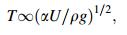
2 Fundamental issues of film thicknessIn order to investigate the thickness effect, our group also performed fundamental research related to metal organic deposition (MOD) coating process parameters, particularly on the influence of different speeds of Czochralski process on the final film thickness. Figure 4 shows the relationship between the withdraw speed and thickness. It can be observed that, with the increase of withdraw speed, the final film thickness initially exhibits an increasing trend. However, as the withdraw speed increases beyond 70 mm/ min, with the film thickness increasing further, the final film thickness undergoes a declining trend. Similarly, the relationship between the density and viscosity is shown in green in Fig. 4. Moreover, we can also observe the relationship between the density and final film thickness of different buffer layers in Fig. 4, as shown with a red line. A theoretical model between the thickness t and withdrawal speed of substrate U was reported [32],
|
(1) |

|
|
|
where α is the viscosity of the coating solution, ρ the density of the solution, and g is the gravitational acceleration. In this case, the exponent is 0.5, which is slightly larger than our case, probably owing to the effect of drying. The above relationship plays an extremely important role in achieving high current.
Furthermore, different heating rates and thicknesses of each layer have a great impact on the critical current density. From Fig. 5, it is evident that with the increase in thickness of each layer, the critical current density of the film shows a downward trend. When the heating rate is less than 5 ℃/min, the critical current density of the film shows a downward trend. When the heating rate is in the range of 5–25 ℃/min, the effect of heating rate on the critical current density is relatively small. Further increasing the heating rate will cause a decrease in the critical current density.

|
|
|
In order to obtain good transport characteristics, one of the main challenges is to maintain a well-aligned crystalline structure along the length of the superconducting film and reduce the number of film defects such as voids, cavities, and second phase as much as possible. In other words, the film must be highly homogeneous. As reported by many researchers, cuprate superconductors usually fall exponentially with the increase in film thickness, which results from the deterioration of microstructure and epitaxial texture.
As evident from Fig. 6, there are three important stages in microstructure evolution. The first stage is characterized by a rapid coarsening of both the grain and the grain boundary (the first 1.7 μm), which corresponds to the degradation of the in-plane texture. Therefore, it is possible that this rapid coarsening of grains and grain boundaries in the first few hundreds of nanometers is related to the initial drop in Jc.

|
|
|
In the second stage (1.7–5.2 μm), the coarsening of both the grain and the grain boundary slows down, which corresponds to a plateau in the deterioration curve of the inplane texture. At a film thickness of approximately 5.2 μm, the third stage begins with a gradual microstructure transition from dendritic grains, which are well connected to equiaxial grains that may have weaker grain connectivity.
Furthermore, in this stage, the effective cross-sectional area for supercurrent flow declines significantly owing to the development and coarsening of grain boundary, and possibly an increased porosity. Consequently, the evolution of microstructure is one of the factors that lead to the decrease of the critical current density. The evolution of superconducting film microstructures cannot be ignored while considering the thickness effect.
Solovyov et al. [34] studied the grain size effect of superconducting films. As shown in Fig. 7, both in physical vapor deposition (PVD) and MOD, with the increase in grain size, the critical current density declines. However, the increase in film thickness is accompanied by an increase in the grain size. In other words, it is important to control the grain size in order to achieve high critical current density.

|
|
|
As evident in Fig. 8, the root mean square (RMS) value of surface roughness of the 200 nm-thick film obtained by pulsed laser deposition (PLD) is 23.6 nm. As the film thickness increases to 1 030 nm, the RMS value of surface roughness is 64.6 nm. For further increase of the film thickness to 1 450 nm, there is a slight increase in the RMS value of surface roughness from 64.6 nm to 68.7 nm. The increase in surface roughness will result in the growth of a-axis grains. In other words, surface roughness is also an important factor resulting in the degradation of critical current density.

|
|
|
The O2+/O3-mode for YBCO films is subject to c-axis orientation and it should be strong enough for a highquality epitaxial YBCO film with a perfect orthorhombic lattice. The O4 mode for YBCO films is subject to a-axis oriented grains.
As we can see from Fig. 9, the peak intensity of the O2+/O3+ mode enhances as the thickness increases. In the case of thinner samples such as YBCO (80 nm) and YBCO (320 nm), the O2+/O3+ mode peaks are nearly absent, whereas they are distinctly perceived in thicker films, such as YBCO (2 000 nm). In other words, with the increase in film thickness, the percentage of a-axis oriented grains increases, resulting in the decrease of critical current density.

|
|
|
Residual stresses will inevitably be induced in a thin film owing to the structural variation and thermal misfit between the thin film and substrate. The structure and properties of films are, therefore, dependent on the residual stress to some degree. Many studies have shown that the residual stress may cause the film to delaminate from the substrate. The emergence of tensile stress will cause the degradation of films, resulting in microcracks, holes, and a-axis grains. It is vital to study the multilayer structure in order to reduce the degradation of the critical current density owing to increasing film thickness.
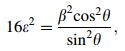
The Williamson Hall method is an old and effective method to analyze the film internal strain ε using X-ray diffraction (XRD) [37]. The relationship of the internal strain ε and the integral breadth β of each (0 0 L) peak of the GdBCO film is expressed as
|
(2) |
where θ is the Bragg angle position of each (0 0 L) peak and λ is the value of X-ray wavelength (λ = 0.154 18 nm).
Figure 10a shows β2cos2θ variation as a function of sin2θ for the GdBCO film with different thicknesses. Using the linear fit slopes obtained in Fig. 10a, the residual stresses calculated using Eq. (1) are 0.101, 0.076, 0.086, and 0.091 for the four GdBCO films, respectively. The corresponding film thicknesses are 200 nm, 1 030 nm, 1 450 nm, and 2 100 nm, respectively.

|
|
|
It is concluded that the thinnest film has the highest residual stress whereas the 1 030 nm-thick film has the lowest residual stress. With further increase in the film thickness, the film residual stresses increase.
In Fig. 10b, monolayer YBCO films thinner than t0 (approximately 1 μm) were under compressive stress [39–41], which would be relieved by the increase in film thickness. There is a tendency for the compressive stress to reduce with the increase in the thickness. For films in the range of 0.5 μm—t0 (approximately 1.0 μm), YBCO thin films have the lowest residual stress, resulting in a nearly free-standing film. As the film thickness is increased beyond t0, tensile stress appears in YBCO films. With the accumulation of tensile stress, cracks, wrinkles, and a-axis emerge, thus affecting the quality of the film. The above analysis is in accordance with Fig. 10a. Consequently, we should manipulate the residual stress in a state of compressive stress in order to reduce the thickness effect.
The 3D strong pinning is produced when vortex lines are chopped into short discontinuous segments by strong pinning defects, which enforce depinning by the bending of vortex segments into critically sized vortex loops, whose diameter is equal to the separation d between pins. The central part of Fig. 11 shows the direction of magnetic field (B), critical current (J) and lorentz force (L), respectively.

|
|
|
Thus, Jc is determined by the pin spacing d and is independent of the film thickness t when d 
It is believed that the decline of pinning force is also an important issue in the investigation of the thickness effect. In order to reduce the thickness effect, artificial pinning centers should be introduced in thick superconducting films.
The O1s spectra consist of two peaks. The main peak at binding energy EB = 528–528.5 eV is related to the O characteristic of the CuO2 plane and CuO chains in superconducting REBCO [43]. The small peak at EB = 530–530.5 eV may be associated with non-superconducting phases [44].
As shown in Fig. 12, the intensity of the two peaks decreases with an increase in the film thickness from 200 nm to 2 100 nm, which indicates that there is less oxygen content for the upper layer of the thicker film compared to the thinner films. Moreover, the curve integral area of the four samples decreases as the film thickness increases from 200 nm to 2 100 nm. This demonstrates that there is less oxygen content for the upper layers of the thicker film. The two trends are not obvious for the 200 nm-thick film and the 1 030 nm-thick film.

|
|
|
However, when the film thickness increases to 1 450 nm, the two trends become obvious. The above analysis implies that the oxygen content is insufficient for the upper layers of the thicker film, especially for a film thicker than 1 030 nm. The oxygen content is different for layers of different depths in a thick film. The oxygen content is almost unchanged for the bottom layer from 0 to approximately 1 030 nm, which is demonstrated in Fig. 12. However, the oxygen content reduces for the upper layers from 1 030 nm to 2 100 nm. The oxygen content reduction is accompanied with the emergence of a-axis grains in the upper layers of the thick film. It indicates that the oxygen deficiency in the upper layers of films beyond a thickness of 1 030 nm mainly results from the emergence of a-axis grains.
5 Copper-rich layers and segregation of elements in multilayer MOD-YBCO coated conductorThe conventional path for increasing the thickness of MOD-based YBCO films has been the deposition and decomposition of multiple thin layers, which are subsequently reacted as a single layer. The individual layers can be prepared with or without rare earth nanoparticle pinning to tune the infield anisotropy [45].
This process has been used at American Superconductor (AMSC) for growing a 2 μm (nominal thickness) film, produced by three individual coating and decomposition steps, with Ic exceeding 500 A/cm-width (77 K, self-field). However, Fig. 13 shows the presence of a copper-rich region between the individual layers.

|
|
|
Through-thickness Ic characterization of fully processed films revealed that Jc of the film above the interface was lower than that below the interface. Through-thickness X-ray texture analysis of the film determined that the decrease in Jc was associated with a reduced YBCO texture in the region above the interface, suggesting that the epitaxial growth of YBCO was partially disrupted as it crossed the copper-rich interface, which was shown in Fig. 13.
Although it has been demonstrated that high throughthickness Jc can be obtained in thick YBCO films (approximately 2 μm) built up from very thin ( < 0.2 μm) layers [47, 48], this method is not consistent with a highrate, low-cost manufacturing process. Copper-rich layers and segregation of elements are also factors resulting in the decrease of critical current density.
6 Methods to improve superconducting performanceExtensive reports on improving superconducting performance via various methods have been published recently. For instance, MacManus-Driscoll et al. [49] performed research linked to rare earth ion size and determined that superior critical current density could be obtained in mixed RE-123 films. Moreover, a multilayer structure such as YBCO/CeO2 is effective in weakening the thickness effect. This multilayer approach makes it possible to fabricate very high critical current coated conductors without being limited by the rapid decrease in Jc for thicker YBCO single-layer films. Finally, co-evaporation process and inclined substrate deposition (ISD) process also obtained good results. 5 μm-thick SmBCO films with the highest Ic value of 1 540 A/cm-width (77 K, self-field) and 8 μm-thick SmBCO films with the highest Ic value of 1 100 A/ cm can be achieved via co-evaporation process and ISD process, respectively.
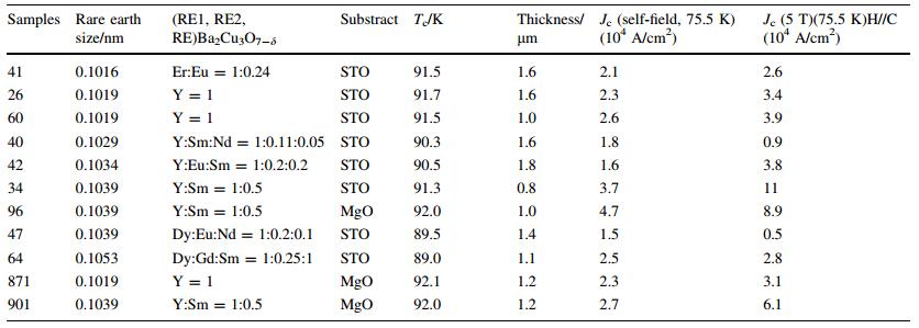
In order to achieve high critical current density, many studies have been performed on rare earth ion size [49]. Table 1 shows the results of the samples prepared in this study. The film with the highest self-field Jc (between 3.7 MA/cm2 and 4.7 MA/cm2) was composed of YSmBCO.
|
As evident from Fig. 14, the improvement of Jc in decorated samples over a range of thickness is the evidence that Ag is effective at creating pinning centers not only in thin films but also in thick films.

|
|
|
As evident from Fig. 15, remarkably high critical current values of 3 963 A/12 mm and 2 797 A/12 mm have been achieved at 3 T and 5 T, respectively, in the 2.2 μm-thick 20% Zr (mole fraction)-added film. These values are more than twice the critical current values obtained for the 0.9 μm-thick 15% Zr (mole fraction)-added film. Hence, heavy doping can improve the superconducting performance of thin films, especially when used in a strong field.

|
|
|
In order to decrease the deterioration of epitaxial texture and microstructure, multilayer structures are introduced in thick superconducting films. For instance, the structure of YBCO/GdBCO consisting of three units of YBCO/GdBCO was obtained via PLD.
Figure 16a shows the structure model of YBCO/GdBCO films. The thickness of each layer is approximately 0.5 μm and YBCO/GdBCO is treated as a unit with a thickness of 1.0 μm. Contrary to a monolayer film, the cross-section of a multilayer film is dense and devoid of a large number of defects, which indicates that residual stress is released periodically by intermittent multilayer deposition method.

Figure 16b shows the structure of YBCO/CeO2. This multilayer approach makes it possible to fabricate very high critical current coated conductors without being limited by the rapid decrease in Jc for thicker YBCO singlelayer films. By an interlayer of CeO2 between the adjacent YBCO layers, the structural defects induced during the increase of thickness of the YBCO layer reduce. This interlayer also provides a starting template for the subsequent growth of a high quality YBCO layer.
As shown in Fig. 17, deposition parameters can be uniformly controlled in a large chamber. Consequently, kilometer-long HTS wires can be fabricated by merely increasing the drum size with significant modification of its basic structure. Use of inexpensive metal elements as evaporation sources can be an additional advantage, reducing the total processing cost of the wires.

|
|
|
Using this method, we can obtain 12 cm-long, 5 μm-thick SmBCO films with the highest Ic value of 1 540 A/ cm-width (77 K, self-field), which corresponds to Jc of 3 MA/cm2. The aforementioned value of Ic is the highest ever reported for any length of HTS film on either single crystal or metallic substrates. Consequently, the thickness effect declines dramatically and high Jc is maintained even as the film thickness approaches 5 μm.
As we can see from Fig. 17, deposition parameters influencing the composition, phase, and texture of the films were optimized via a unique combinatorial method that is broadly applicable to co-evaporation of other promising complex materials containing several cations. Unlike previous reports, no exponential decay of Ic with increasing thickness is observed in this study for samples fabricated under optimized conditions. The lack of any degradation in the structural properties with increasing thickness plays a critical role in maintaining high Jc, and consequently high Ic in these thick films. The EDDC technique and the combinatorial method prove invaluable in the fabrication of other complex, high-performance, and functional materials [52].
We can see clearly from Fig. 18 that the critical current density of DyBCO films with a thickness 6 μm is close to that of thinner DBCO films with a thickness of 2 μm, whose Jc ranges from 1.6 MA/cm2 to 2.6 MA/cm2. This indicates that the critical current density does not decline significantly with an increase in thickness. In other words, the thickness effect is weakened.

|
|
|
ISD yields a non-zero component of the growth direction parallel to the DyBCO (a, b)-plane since DyBCO grows on a faceted MgO surface and avoids the a-axis growth. Highly biaxially textured DyBCO films at all thicknesses can be obtained; thus, no significant decrease in the critical current density occurs with the increase in film thickness. Therefore, the ISD technology offers a unique possibility to overcome thickness limitations in coated conductor technology.
7 ConclusionsThe thickness dependence of Jc in the second generation superconducting films is reviewed in the present paper. It is believed that the phenomenon of thickness effect is caused by a series of factors such as the emergence of a-axis oriented grains, oxygen deficiency, evolution of microstructure, segregation of elements, residual stress, surface roughness, and decline of pinning force, etc. Recent progress in enhancing the superconducting performance of thin films especially in terms of critical current density is summarized. Further, with the increase in film thickness, more artificial defects are required as effective pinning centers for a higher current density. It is concluded that the artificial multilayer architecture is very helpful in maintaining the epitaxial texture of REBCO films, which allows an integrated understanding of the thickness effect.
Acknowledgements This work was supported in part by Shanghai Key Laboratory of High Temperature Superconductors (Grant No. 14DZ2260700), the Science and Technology Commission of Shanghai Municipality (Grant Nos. 13111102300 and 14521102800), and the National Natural Science Foundation of China (Grant Nos. 51572165, 11174193 and 51202141).| 1. | Shiohara Y, Yoshizumi M, Takagi Y, et al(2013)Future prospects of high Tc superconductors-coated conductors and their applications.Phys C Superconduct 484, 1-5 doi:10.1016/j.physc.2012.03.058 |
| 2. | Ko KP, Choi SM, Kim YC, et al(2011)Strongly enhanced flux pining of GdBCO coated conductors with BaSnO3 nanorods by pulsed laser deposition.Phys C 471, 940-943 doi:10.1016/j.physc.2011.05.094 |
| 3. | Abiru K, Shingai Y, Konishi M, et al(2011)30 mm wide process of GdBCO PLD/clad-type textured metal substrates.Phys C 471, 924-928 doi:10.1016/j.physc.2011.05.090 |
| 4. | Carmine S, Matteo A, Andrea L, et al(2014)Progresses and challenges in the development of high-field solenoidal magnets based on RE123 coated conductors.Supercond Sci Technol 27, 103001 doi:10.1088/0953-2048/27/10/103001 |
| 5. | Usoskin A, Betz U, Dietrich R, et al(2016)Long HTS coated conductor processed via large-area PLD/ABAD for high-field applications. IEEE Trans Appl Supercond 26(3), 7500904 |
| 6. | Rutt A, Schneider T, Kirchhoff L, et al(2016)Ultrahigh-speed pulsed laser deposition of YBCO layer in processing of long HTS coated conductors. IEEE Trans Appl Supercond 26(3), 6602304 |
| 7. | Martynova I, Tsymbarenko D, Kamenev A, et al(2016)Solution deposition of ultrasmooth alumina on long-length metallic substrate for, 2G superconducting tapes.Mater Res Bull 78, 64-71 doi:10.1016/j.materresbull.2016.02.014 |
| 8. | Song H, Brownsey P, Zhang Y, et al(2013)2G HTS coil technology development at superpower.IEEE Trans Appl Supercond 23(3), 4600806 doi:10.1109/TASC.2012.2233837 |
| 9. | Martin W, Li X, Sathyamurthy S, et al(2013)Second generation wire development at AMSC.IEEE Trans Appl Supercond 23(3), 6601205 doi:10.1109/TASC.2012.2235495 |
| 10. | Vyacheslav FS, Li Q, Rupich M, et al(2013)New pinning strategies for second-generation wires.IEEE Trans Appl Supercond 23(3), 6600905 doi:10.1109/TASC.2012.2234322 |
| 11. | Holesinger TG, Maiorov B, Ugurlu O, et al(2009)Microstructural and superconducting properties of high current metal-organic chemical vapor deposition YBa2Cu3O7-δ coated conductor wires.Supercond Sci Technol 22, 045025 doi:10.1088/0953-2048/22/4/045025 |
| 12. | Shiohara Y, Taneda T, Yoshizumi M(2012)Overview of materials and power applications of coated conductors project.Jpn J Appl Phys 51(1), 010007 doi:10.1143/JJAP.51.010007 |
| 13. | Luborsky FE, Kwasnick RF, Borst K, et al(1988)Reproducible sputtering and properties of Y-Ba-Cu-O films of various thicknesses.J Appl Phys 64(11), 6388-6391 doi:10.1063/1.342051 |
| 14. | Mogro-Campero A, Turner LG, Hall EL, et al(1990)Film thickness dependence of critical current density and microstructure for epitaxial YBa2Cu3O7-x films.Supercond Sci Technol 3, 62-66 doi:10.1088/0953-2048/3/2/002 |
| 15. | Foltyn SR, Tiwari P, Dye RC, et al(1993)Pulsed laser deposition of thick YBa2Cu3O7-δ films with Jc ≥1 MA/cm2.Appl Phys Lett 63, 1848-1850 doi:10.1063/1.110653 |
| 16. | Foltyn SR, Civale L, Macmanus-Driscoll JL, et al(2007)Materials science challenges for high-temperature superconducting wire.Nat Matter 6, 631-642 doi:10.1038/nmat1989 |
| 17. | Dam B, Huijbregtse JM, Klaassen FC, et al(1999)Origin of high critical currents in YBa2Cu3O7-δ superconducting thin films.Nature 399, 439-442 doi:10.1038/20880 |
| 18. | Huijbregtse JM, Dam B, Vander GeestRCF, et al(2000)Natural strong pinning sites in laser-ablated YBa2Cu3O7-δ thin films.Phys Rev B 62(2), 1338-1349 doi:10.1103/PhysRevB.62.1338 |
| 19. | Dam B, Huijbregtse JM, Rector JH(2002)Strong pinning linear defects formed at the coherent growth transition of pulsed-laserdeposited YBa2Cu3O7-δ films.Phys Rev B 65, 064528 doi:10.1103/PhysRevB.65.064528 |
| 20. | Kang BW, Goyal A, Lee DF, et al(2002)Comparative study of thickness dependence of critical current density of YBa2Cu3O7-δ on (100) SrTiO3 and on rolling-assisted biaxially textured substrates.J Mater Res 17(7), 1750-1757 doi:10.1557/JMR.2002.0259 |
| 21. | Wang X, Wu JZ(2007)Effect of temperature and magnetic field on the thickness dependence of the critical current density of YBa2Cu3O7-x films.Phys Rev B 76, 184508 doi:10.1103/PhysRevB.76.184508 |
| 22. | Tran DH, Putri WBK, Wei CH, et al(2012)Thickness dependence of critical current density in GdBa2Cu3O7-δ thin films with BaSnO3 addition.J Appl Phys 111, 07D714 doi:10.1063/1.3676618 |
| 23. | Aytug T, Paranthaman M, Specht ED, et al(2010)Enhanced flux pinning in MOCVD-YBCO films through Zr additions: systematic feasibility studies.Supercond Sci Technol 23, 014005 doi:10.1088/0953-2048/23/1/014005 |
| 24. | Feldmann DM, Larbalestier DC, Feenstra R, et al(2003)Throughthickness superconducting and normal-state transport properties revealed by thinning of thick film ex situ YBa2Cu3O7-x coated conductors.Appl Phys Lett 83(19), 3951-3953 doi:10.1063/1.1625103 |
| 25. | Emergo RLS, Wu JZ, Aytug T, et al(2004)Thickness dependence of superconducting critical current densityin vicinal YBa2Cu3O7-δ thick films.Appl Phys Lett 85(4), 618-620 doi:10.1063/1.1775882 |
| 26. | Foltyn SR, Jia QX, Arendt PN, et al(1999)Relationship between film thickness and the critical current of YBa2Cu3O7-δ coated conductors.Appl Phys Lett 75(23), 3692-3694 doi:10.1063/1.125431 |
| 27. | Jia QX, Foltyn SR, Arendt PN, et al(2002)High-temperature superconducting thick films with enhanced supercurrent carrying capability.Appl Phys Lett 80(9), 1601-1603 doi:10.1063/1.1455143 |
| 28. | Sanchez A, Navau C, Del-Valle N, et al(2010)Self-fields in thin superconducting tapes: implications for the thickness effect in coated conductors.Appl Phys Lett 96, 072510 doi:10.1063/1.3315893 |
| 29. | Hengstberger F, Eisterer M, Weber HW(2010)Thickness dependence of the critical current density in superconducting films: a geometrical approach.Appl Phys Lett 96(2), 022508 doi:10.1063/1.3290254 |
| 30. | Rostila LJ, Mikkonen R(2007)Self-field reduces critical current density in thick YBCO layers.Phys C 451, 66-70 doi:10.1016/j.physc.2006.10.008 |
| 31. | Rupich WM, Li X, Sathyamurthy S, et al(2011)Advanced development of TFA-MOD coated conductors.Phys C 471, 919-923 doi:10.1016/j.physc.2011.05.089 |
| 32. | Guglielmi M, Colombo P, Peron F(1992)Dependence of thickness on the withdrawal speed for SiO2 and TiO2 coatings obtained by the dipping method.J Mater Sci 27, 5052-5056 doi:10.1007/BF01105273 |
| 33. | Zhou H, Majorov B, Baily SA, et al(2009)Thickness dependence of critical current density in YBa2Cu3O7-δ films with BaZrO3 and Y2O3 addition.Supercond Sci Technol 22, 085013 doi:10.1088/0953-2048/22/8/085013 |
| 34. | Solovyov VF, Wiesmann H, Wu LJ, et al(1999)High rate deposition of, 1999, 5 μm thick YBa2Cu3O7 films using the BaF2 ex-situ post annealing process.IEEE Trans Appl Supercond 9(2), 1467-1470 doi:10.1109/77.784669 |
| 35. | Wang Y, Xu D, Li YJ, et al(2013)Dependencies of microstructure and stress on the thickness of GdBa2Cu3O7-δ thin films fabricated by RF sputtering.Nanoscale Res Lett 8, 304-312 doi:10.1186/1556-276X-8-304 |
| 36. | Zeng L, Lu YM, Liu ZY, et al(2012)Surface texture and interior residual stress variation induced by thickness of YBa2Cu3O7-δ thin films.J Appl Phys 112, 053903 doi:10.1063/1.4750037 |
| 37. | Jiang HG, Ruehle M, Lavernia EJ(1999)on the applicability of the X-ray diffraction line profile analysis in extracting grain size and microstrain in nanocrystalline materials.J Mater Res 14(2), 549-559 doi:10.1557/JMR.1999.0079 |
| 38. | Lin JX, Yang WT, Gu ZH, et al(2015)Improved epitaxial texture of thick YBa2Cu3O7-δ/GdBa2Cu3O7-δ films with periodic stress releasing.Supercond Sci Technol 28, 045001 doi:10.1088/0953-2048/28/4/045001 |
| 39. | Ross JDJ, Pollock HM, Pivin JC, et al(1987)Limits to the hardness testing of films thinner than, 1987, 1 μm.Thin Solid Films 148(2), 171-180 doi:10.1016/0040-6090(87)90155-6 |
| 40. | Müller K(1987)Stress and microstructure of sputter-deposited thin films: molecular dynamics investigations.J Appl Phys 62(5), 1796-1799 doi:10.1063/1.339559 |
| 41. | Park J, Lee SY(1999)Orientation transition in a thick laser deposited YBa2Cu3O7-x film observed by glancing angle X-ray diffraction.Phys C Superconduct 314, 112-116 doi:10.1016/S0921-4534(99)00030-1 |
| 42. | Kes PH, Tsuei CC(1983)Two-dimensional collective flux pinning, defects, and structural relaxation in amorphous superconducting films.Phys Rev B 28(9), 5126-5139 doi:10.1103/PhysRevB.28.5126 |
| 43. | Beyer J, Schurig T, Menkel S, et al(1995)XPS investigation of the surface composition of sputtered YBCO thin films.Phys C 246, 156-162 doi:10.1016/0921-4534(95)00159-X |
| 44. | Rajasekar P, Chakraborty P, Bandyopadhyay SK, et al(1998)X-ray photoelectron spectroscopy study of oxygen and argon annealed YBa2Cu3O7-δ.Mod Phys Lett B 12, 239-245 doi:10.1142/S0217984998000317 |
| 45. | Chen ZJ, Feldmann DM, Larbalestier DC, et al(2007)Top-down and bottom-up through-thickness current anisotropy in a bilayer YBa2Cu3O7-x film.Appl Phys Lett 91(91), 052508 |
| 46. | Martin WR, Li XP, Thieme C, et al(2010)Advances in second generation high temperature superconducting wire manufacturing and R&D at American Superconductor Corporation.Supercond Sci Technol 23, 014015 doi:10.1088/0953-2048/23/1/014015 |
| 47. | Nakaoka K, Matsuda J, Kitoh Y, et al(2007)Influence of starting solution composition on superconducting properties of YBCO coated conductors by advanced TFA-MOD process.Phys C Superconduct Appl 463-465, 519-522 doi:10.1016/j.physc.2007.04.264 |
| 48. | Izumi T, Yoshiyumi M, Miura M, et al(2008)Research and development of reel-to-reel TFA-MOD process for coated conductors.Phys C Superconduct 468, 1527-1530 doi:10.1016/j.physc.2008.05.270 |
| 49. | MacManus-Driscoll JL, Foltyn SR, Maiorov B, et al(2005)Rare earth ion size effects and enhanced critical current densities in Y2/3Sm1/3Ba2Cu3O7-x coated conductors.Appl Phys Lett 86, 032505 doi:10.1063/1.1851006 |
| 50. | Dang VS, Mikheenko P, Sarkar K, et al(2011)Combination of Ag substrate decoration with introduction of BaZrO3 nano-inclusions for enhancing critical current density of YBa2Cu3O7 films.J Supercond Nov Magn 24, 505-509 doi:10.1007/s10948-010-0981-8 |
| 51. | Selvamanickam V, Heydari GharahcheshmehM, Xu A, et al(2015)Critical current density above, 2015, 15 MA cm-2 at 30 K, 3 T in 2.2 μm thick heavily-doped (Gd, Y)Ba2Cu3Ox superconductor tapes.Supercond Sci Technol 28, 072002 doi:10.1088/0953-2048/28/7/072002 |
| 52. | Kim HS, Ha HS, Youm D, et al(2014)Ultra-high performance, high-temperature superconducting wires via cost-effective, scalable, co-evaporation process. Sci Rep 4, 4744 |
| 53. | Dürrschnabel M, Aabdin Z, Bauer M, et al(2012)DyBa2Cu3O7-x superconducting coated conductors with critical currents exceeding, 2012, 1 000 A cm-1.Supercond Sci Technol 25, 105007 doi:10.1088/0953-2048/25/10/105007 |