 2014, Vol. 2
The article information
- Zai-Fang Zhang, Yuan Liu, Xiao-Song Wu, Shu-Lin Kan
- Integrated color defect detection method for polysilicon wafers using machine vision
- Advances in Manufacturing, 2014, 2(4): 318-326
- http://dx.doi.org/10.1007/s40436-014-0095-9
-
Article history
- Received: 2014-03-17
- Accepted: 2014-11-11
- Published online: 2014-12-07


Polysilicon wafer has the characteristics of abundant raw materials, mature manufacturing technology, stable performance, and high photoelectric conversion efficiency, which is widely used in solar cell industry [1, 2]. In polysilicon wafer production, plasma enhanced chemical vapor deposition (PECVD) is an important and widelyapplied process because it has great advantages on quality and cost [3, 4, 5]. After going through film coating based on PECVD, there are an amount of unqualified products with edge discoloration or color difference on their surfaces. However, these defects are influenced by the defect characteristics and surface textures of polisilicon wafers, hence they cannot be effectively detected by the general detection methods. The detection for these defects mostly relies on manual inspecting in the practical production.
The surface color and texture features of polysilicon wafer are very complex after the technical processing of PECVD [6, 7]. They have mixed growth direction of crystalline grain and different coating colors. It is very difficult to detect under the influences of these characteristics. Due to the physiological characteristics of human beings, long-time repeated labor and other subjective factors, the way of manual detection is difficult to ensure high efficiency and accuracy. That greatly impacts the efficiency and quality of polysilicon wafer production. Machine vision detection using computer vision to replace manual vision is an emerging technology, which has been widely applied in agriculture and industry [8, 9, 10, 11]. Nowadays, machine vision detection method is going to be the trend in the mass production of silicon wafers. Machine vision was used to detect the defects of regular-textured monocrystalline silicon wafers [12]. However, the detection accuracy is not high when it is applied in the irregular-textured polysilicon wafers. A visual inspection approach was developed based on Fourier transform for detecting the linear or columnar defects (such as cracks) of polysilicon wafers [13]. The color defects of polysilicon wafers (e.g., edge discoloration) are needed for further research, which have more complex characteristics than the defects of monocrystalline silicon wafers or the linear defects of polysilicon wafers. In this paper, a machine-vision-based detection approach integrating fuzzy clustering, classifying and region growing is proposed for identifying the color defects of polysilicon wafers.
This paper introduces three typical color defects of polysilicon wafers, proposes a new holistic method to identify these defects, and discusses the detailed process of the method. Finally, a machine vision defection system is developed and applied in a real-world case. 2 Color defects
Due to various factors, such as raw materials, deposition equipment, processing technology, system control and so on, some color defects may merge after the PECVD process. These defects can change the conductivity of solar cells, the grain flatness, the current stability, the service life, and seriously affect the performance and quality of the final solar cell products. In this paper, the typical color defects including edge discoloration, color inaccuracy and color non-uniformity are discussed in detail. 2.1 Edge discoloration
Edge discoloration of polysilicon wafer means that there is a large color difference between the edge and the inner region. Edge discoloration generally concentrates on the edge of wafer, and occupies a small area. Three colors including red, yellow and white are mainly shown in the defects. A polysilicon wafer with edge discoloration is given in Fig. 1, and color change can be easily observed on the edge.
 |
| Fig. 1 Edge discoloration on a polysilicon wafer (the black strips are conveyor belts) |
The primary qualified standard of polysilicon wafers is that their colors must be blue or in the blue color range. The color range can be divided into nine degrees, as shown in Fig. 2. A quantitative method should be developed in order to determine the value of wafer color. If the value is not in the range of "blue", the wafer color will not be accurate and cannot meet the production requirement.
 |
| Fig. 2 Color system of qualified wafers |
The surface color of a wafer may be different in the different areas, which means that the color is non-uniform. For example, nearly half of the surface color of a wafer is blue and the part of middle is dark blue (see Fig. 3). Furthermore, a small piece of region color may be obviously different contrast with the entire wafer, which means that it is also non-uniform even though the wafer looks consistent.
 |
| Fig. 3 Non-uniform color wafer |
The color defect detection method of polysilicon wafers mainly consists of five stages, including image pre-processing, edge fitting, HSV model transforming, color detecting based on fuzzy color clustering and classifying, and outputs (see Fig. 4).
 |
| Fig. 4 Framework of the detection method |
Wafer images taken by CCD camera include the foreground and background. A processing method is needed to extract pure wafer images for facilitating color defect detection. There is a greater difference in color between the image foreground (i.e., silicon and conveyor belts are dark and they have similar colors) and the image background (i.e., rear panel). Considering this characteristic, the general gray-value segmenting method can be used to separate the foreground from the background. 3.2 Edge fitting
Generally the edge of wafer image should be a line. The fluctuation of taking images and image pre-processing may not make the edge sharp and even bent, which is very unfavorable for accurate detection. A mean-value method is used to fit edge for restraining fluctuation and improving position accuracy. The four straight edges can be obtained after fitting edge. Wafer is then accurately positioned through corners which are identified by using the intersection of four edges, as given in Fig. 5. Some shape parameters (such as width and length of the wafer) can be identified, which have important effects on detection calculation.
 |
| Fig. 5 Wafer positioning |
Furthermore, edge area should be defined when detecting edge color. Three wafer templates are first built considering three types of wafers, i.e., rectangle wafer, rounding wafer, and chamfering wafer. Edge area is obtained by applying these templates on actual wafers by affine transformation. An example of rectangle wafer with dividing lines is given in Fig. 6. Therefore, the edge area can be easily defined by the region among these lines.
 |
| Fig. 6 Defining edge area of a rectangle wafern |
The image obtained by CCD camera is true color image (i.e., RGB image), in which the color detection and calculation process are more complex. For avoiding the effects of polysilicon wafers’ irregular textures and facilitating data processing, an HSV color model is used to express wafer color.
The HSV model includes three elements: hue, saturation and value. HSVcolor parameters can be obtained fromRGBcolor parameters by using nonlinear transformation [14]. Set (r, g, b) be real numbers between 0 and 1, which are the color coordinates of red, green and blue, respectively. Through synthetically comparing all the values of r, g and b, the maximumand theminimumvalues can be identified. Let m, n be the maximum value and the minimum value among all the values of r, g and b, respectively. The color is expressed by the color coordinate value x = (xH; xS; xV) in the HSV space, where xH; xS; xV are the channel values, xH [[0, 360°), and xS; xV ∈ [0; 1°]. Three empirical formulas can be given as
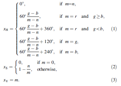
For the standardization of all related information, H, S, V channel values can be expressed between 0 and 255 as the normalized values through the linear transformation. 3.4 Edge discoloration detecting
After pre-processing and edge fitting, the edge area of polysilicon wafer image would be transformed into an HSV color model. A fuzzy clustering method is used to detect edge discoloration based on establishing the membership function of each color type. Pixels in the color model are classified into the four color types including red, yellow, white and normal. The color of normal is blue because qualified wafer color is blue. The wafer has edge discoloration and possible color type can be identified by summing the number of pixels of each color type.
Let A1, A2, A3, A4 be red edge, yellow edge, normal edge and white edge respectively, and YK(Aj) be their membership functions, where K = H, S, V, j = 1, 2, 3, 4. According to color discrimination by human vision, the membership function can be identified by unequal interval dividing the variable ranges of the three channels H, S, V. Membership functions of red, yellow, normal edges in H channel are heuristically given as
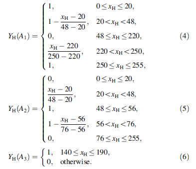
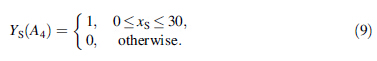
The control parameters in the above formulas are from the judgments of the engineers on the three kinds of colors. Since white is independent of hue and it relies on saturation and tone, the membership function of white edge in H channel is

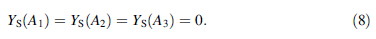
Just like H channel has no contribution on the white membership, there is no contribution in S channel and V channel for red, yellow, and normal. Therefore, membership functions of the three colors in S channel are
In the HSV space, H and S describe the color and V describes the brightness. The color-independent channel V can be stripped out for detecting color inaccuracy. For the pixels of the qualified wafers, H value is generally in the range of 140-190 (see Fig. 7). With the color of the silicon wafer changing from light blue to dark blue, the H value gradually increases, while the S value changes little. The S values of different wafers are almost the same by comparing a large number of wafer images. Therefore, the H value is selected to express the pixel color. It successfully changes the original description of color from the three-dimensional RGB space into the one-dimensional space, which has obviously high efficiency.
 |
| Fig. 7 Hue and color range of wafer |
Through comparing and analyzing a large number of wafers, it is found that the H value distributions of all image pixels are very concentrated and the standard deviation is usually less than 1.5. That means that the color value dC of the entire wafer can be represented by the mean value hij of all the pixels in H channel:
Set the appropriate upper and lower boundaries to identify the color accuracy (cA)
The data standard deviation is the easiest way to judge whether its distribution is uniform. However, the approach only examines the statistical summary information of the sample but does not take into account time and space relationships among the data. The color uniformity is associated with the color values and their distributions. A pixel color is close to other nearby pixels, which means that this region is more uniform.
The region growing method provides a useful way for detecting color uniformity [15, 16]. Firstly, an initial pixel is merged adjacent pixels with similar color into one large area. Secondly, the boundary pixels of this area are taken a further identification until every pixel has been processed. Finally, the entire image has been identified. A big region with similar color can be obtained on the H channel, which is quite different from that outside the region. Comparing the area of the region with that of the entire wafer, it shows that the entire wafer is uniform if the ratio is more than a pre-defined threshold (e.g., 85% is an ideal boundary).
There is a special case that an area which contains some holes will appear after the region growth. An obvious color difference exists between these holes and the growth areas, where the case is deemed as color non-uniformity. Therefore, a judgment should be done. If the hole is relatively big (i.e., over 2% of the surface area of the wafer) and the xH values of holes are quite different from those of the growth area, this will show that the wafer has an obvious hole and it is seen as unqualified.
The area ratio r of the growth region and the entire region is given as
Compared r with the uniform threshold (T) as
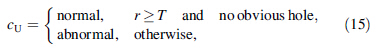
The predefined parameters are generally determined based on the engineers’ knowledge and experience. These parameters may be adjusted according to the different quality requirements and different orders from the customers. For example, the T in Eq. (15) may be set as 2% in the production of an order but it may be set as 4% in another order. That is related to different quality control requirements in the two orders. 4 Machine vision detection system development and application
An online vision detection system is developed for the polysilicon wafer production in a large domestic solar energy enterprise (see Fig. 8). The color defects of polysilicon wafers can be efficiently and accurately detected by the system, which includes identifying edge discoloration, color inaccuracy and color non-uniformity, and classifying the polysilicon wafers into qualified and non-qualified types automatically. The hardware system includes:
(i) Feeding device. It delivers polysilicon wafers in the feed box into transportation system.
 |
| Fig. 8 Color defect detection system for polysilicon wafers |
(ii) Transportation system. It delivers the wafers to the appropriate location by using PLC control, gets the current position information and systemstatus of the wafers by using the triggers, and handles communicating with vision system.
(iii) Vision system. It includes hardware and software. The hardware includes lenses, cameras, image acquisition cards, IPC, data transmission system, and so on. The software function is image detection and identification, which includes image achieving, image processing, defect detecting, result output and storage, status controlling and parameter adjusting.
(iv) Sorting and blanking device. It performs the sorting operation and transports the wafers to the blanking box according to control signals.
(v) Emergency processing modules. It provides an interface to the manual operations in the emergency situation, such as artificially stop and reset.
Color discoloration is taken as an example to illustrate the detailed detection process. The image in Fig. 1 is transformed into an HSV channel image and the threechannel image segmentation is given in Fig. 9.
 |
| Fig. 9 Three channels in HSV space |
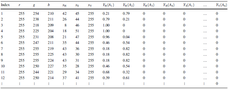
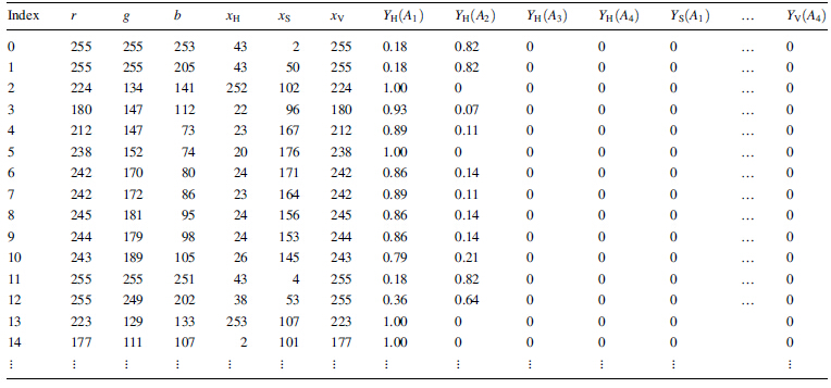
The outputs of the pixel color type and membership degree of left side and bottom side are shown in Tables 1 and 2. The pixel color is classified into four types, and the results are shown in Figs. 10(a) and (b), respectively. The classifying threshold value c is set as 800. It is concluded that the wafer edges have changed color and the color types are yellow and red (see Fig. 10 (c)). Obviously, the other two sides also have changed color.
 |
| Fig. 10 Results of edge discoloration detection |
The color accuracy detection result of a wafer is given in Fig. 11(a), where the color mean is 156.6 and the color degree is 3 in the color system of polysilicon wafers. It shows that the wafer’s color is qualified.
 |
| Fig. 11 Results of color accuracy and uniformity detection |
The color uniformity detection result of a wafer is given in Fig. 11(b), where the wafer has a "hole" defect and the uniformity ratio is 94.8%. The hole is in the red wire frame of upper right corner. Although the ratio is very high, the wafer is still deemed as an unqualified one for having a "hole" defect according to Eq. (15). 5 Conclusions
Color defect detection of polysilicon wafers is implemented by a new fuzzy clustering method and classifying method based on an HSV color model. The RGB images of wafers were firstly transformed into different HSV channel images. This transform can effectively weaken or eliminate the disturbances of irregular texture of polysilicon wafer. The fuzzy clustering method was proposed to detect edge discoloration through edge feature extracting and membership function. A mean-value classifying method and a region growing method are used for detecting color inaccuracy and color non-uniformity, respectively. An online machine vision detection system for a polysilicon wafer manufacturing enterprise was developed and validated by an actual application. Further work would consider the parameter automatic adjustment mechanism for different orders and different qualified criteria. Meanwhile other defects or new requirements, e.g., fingerprints, roller printing and batch classification, will be studied, and corresponding functions will be added into the system.
Acknowledgements The project was supported by the National Natural Science Foundation of China (Grant Nos. 51205242, and 51075261) and the Shanghai Science and Technology Innovation Action Plan, China (Grant No. 13111102900). The authors express sincere appreciation to the anonymous referees for their helpful comments to improve the quality of the paper.| 1. | Stupca M, Alsalhi M, Saud TA et al (2007) Enhancement of polycrystalline silicon solar cells using ultrathin films of silicon nanoparticle. Appl Phys Lett 91(6):063107 |
| 2. | Karunagaran B, Chung SJ, Velumani S (2007) Effect of rapid thermal annealing oil the properties of PECVD SiNx thin films. Mater Chem Phys 106(1):130-133 |
| 3. | Yoo JS, So JH, Yu GJ et al (2011) Study on hydrogenated silicon nitride for application of high efficiency crystalline silicon solar cells. Solar Energy Mater Solar Cells 95(1):7-10 |
| 4. | Otani T, Hirata M (2003) High rate deposition of silicon nitride films by APCVD. Thin Solid Films 442:44-47 |
| 5. | Schlemm H, Mai A, Roth S et al (2003) Industrial large scale silicon nitride deposition on photovoltaic cells with linear microwave plasma sources. Surf Coat Technol 208:174-175 |
| 6. | Zhang Y, Wang Y, Cai M et al (2012) Metallization introduced corrosion and parylene protection of surface micromachined polysilicon film with submicron capacitive gap. Microelectron Eng 97(9):20-25 |
| 7. | Wang S, Lennon A, Tjahjono B et al (2012) Overcoming overplating problems for PECVD SiNx passivated laser doped p-type multi-crystalline silicon solar cells. Solar Energy Mater Solar Cells 99(1):226-234 |
| 8. | Cavaliere P, Santis AD, Panella F et al (2009) Thermo elasticity and CCD analysis of crack propagation in AA6082 friction stir welded joints. Int J Fatigue 31(2):385-392 |
| 9. | Jimenez AR, Ceres R, Pons JL (2000) A survey of computer vision methods for location fruit on trees. Trans ASAE 43(6):1911-1920 |
| 10. | Liu P, Tu K, Pan QL et al (2009) Persimmon's surface defect recognition based on machine vision fuzzy clustering. Acta Opt Sin 29(s2):138-144 |
| 11. | Wu GF, Xu K, Yang ZL (2010) The online inspection technology of steel plate surface quality. Science Press, Beijing |
| 12. | Sheng XC (2011) Research on solar mono-crystanine silicon wafer surface quality inspection based on image processing. Dissertation, Chang'an University |
| 13. | Tsai DM, Wu SC, Li WC (2012) Defect detection of solar cells in electroluminescence images using Fourier image reconstruction. Solar Energy Mater Solar Cells 99(1):250-262 |
| 14. | Chan TF, Kang SH, Shen JH (2001) Non-texture inpainting by curvature driven diffusions (CDD). J Vis Commun Image Represent 12(4):436-449 |
| 15. | Lachance S, Bauer R, Warkentin A (2004) Application of region growing method to evaluate the surface condition of grinding wheels. Int J Mach Tools Manuf 44(7/8):823-829 |
| 16. | Yau HT, Lin YK, Tsou LS et al (2008) An adaptive region growing method to segment inferior alveolar nerve canal from 3D medical images for dental implant surgery. Comput Aided Design Appl 5(5):743-752 |