 2023, Vol. 34


b School of Chemistry and Physics, Centre of Materials Science, Queensland University of Technology, Brisbane 4001, Australia;
c Chongqing Institute of Green and Intelligent Technology, Chinese Academy of Sciences, Chongqing 400714, China
With the rapid expansion of chemical plants and automobiles, NO2, as one notorious exhausted pollutant, has fueled people's ever-increasing concern [1]. NO2 not only plays a major role in serious atmospheric pollution including acid rain, heavy smog, and ozone, but also severely harms to human respiratory system [2]. The threshold limit value (TLV) of NO2 gas is estimated as 3 ppm for people according to the American Conference of Governmental Industrial Hygienists (ACGIH) [3]. And it has been evidenced that even ppb-level NO2 still threatens human health [4]. Therefore, it is highly urgent to develop effective, sensitive, and real-time NO2 sensors at ppm level or below. To this end, conventional gas sensors based on metal oxide semiconductors have been pioneering their efforts with high response and facile fabrication [5-10]. Nevertheless, the elevated operating temperature, low selectivity, and incompatibility with flexible and wearable optoelectronics frustrated their practicability [11].
In the last decade, two-dimensional (2D) nanomaterials have drawn great attention as the active pivot for gas sensors [12-15]. Unfortunately, previous reports have witnessed impenetrable barriers confronted by some 2D candidates (rGO, WSe2, WS2, phosphorene, MXene) for gas sensing such as susceptibility to humidity interference, weak selectivity, and/or fragile environment stability [16-20]. To overcome these dilemmas, introducing additives or modifications (e.g., noble metal doping and heterojunction construction) and adjuvant light excitation have been verified as feasible strategies [21-24], undesirably accompanied with costly device preparation and test equipment as well as complex material synthesis. Therefore, it is significant to develop new 2D materials based gas sensors with high sensitivity, selectivity, and stability. Recently, Ou et al. have proposed one novel NO2 sensor based on SnS2 with high sensitivity, and nice reversibility [25]. However, high operating temperature (120 ℃) hampered its further application in flexible electronics. Of other 2D candidates, semiconducting binary metal chalcogenides AVBVI (A: As, Sb, Bi; B: S, Se, Te), have attracted considerable interest in the fields of thermoelectric devices, optoelectronic devices, and hydrogen storage materials due to their unique physico-chemical properties [26-31]. Particularly, bismuth selenide (Bi2Se3) is a well-known n-type topological insulator with a direct narrow bandgap (0.3–0.335 eV) and chemical stability at room temperature [32]. Besides, the typical characteristics, including the layered structure, large specific surface area, abundant adsorption sites, high carrier mobility, and brilliant mechanical flexibility enable Bi2Se3 an ideal gas-sensing material taking into account the low operating temperature, large sensitivity, good compatibility, and high efficiency [33-35]. More importantly, the inherent hydrophobicity of Bi2Se3 indicates a fantastic humidity tolerance within ambient environments [36]. Nevertheless, as far as we know, chemical gas sensors based on Bi2Se3 have not been reported thus far.
Motivated by the stated facts above, this work detailed the first demonstration of nanoplate Bi2Se3 film for high-performance NO2 gas sensor at room temperature especially under the flexible substrate (see the Supporting information for details on materials preparation, device fabrication, and test procedure (Figs. S1 and S2 in Supporting information)). The flexible Bi2Se3 sensor exhibited a gradient response with NO2 concentration ranging from 100 ppb to 12.5 ppm at room temperature. Various relative humidity and bending angles were leveraged to verify the operation compatibility of the flexible sensors. Furthermore, a series of density functional theory (DFT) calculations on charge density difference (CDD) and density of states (DOS) were employed to reveal the underlying sensing mechanism.
In this work, Bi2Se3 nanoplates were grown by the chemical vapor deposition (CVD) method via a horizontal tube furnace as shown in Fig. 1a. The flexible device with Bi2Se3 nanoplates grown on copper interdigital electrodes (IDEs) pre-patterned on polyimide (PI) substrate was schematically exhibited in Fig. 1b. And the optical photograph of the as-prepared Bi2Se3 device and SEM image of the sensing area were displayed in Fig. S3 (Supporting information). As for the characterization of the as-synthesized Bi2Se3, firstly, randomly-distributed and free-standing Bi2Se3 nanoplates were observed from the SEM image (Fig. 1c). A large coverage and high yield of Bi2Se3 nanoplates were achieved. An approximate atomic ratio of Bi to Se at 2:3 from EDS spectra (Fig. S4 in Supporting information) was consistent with Bi2Se3 configuration. Moreover, the TEM image (Fig. 1d) exhibited a clear nanoplate structure of the obtained Bi2Se3 with the lateral size of ~350 nm. High-resolution TEM image (Fig. 1e) and the relevant fast fourier transform (FFT) forms revealed the lattice spacings of 0.30 nm corresponding to the crystal plane of (015) for Bi2Se3, indicative of the successful synthesis. Afterwards, XRD measurements were employed to verify the crystalline structure of the Bi2Se3 nanoplates in Fig. S5 (Supporting information). After deducting the background of the PI substrate underneath, the main diffraction peaks at 9.1°, 18.3°, 29.2° and 47.3° were respectively assigned to (003), (006), (015) and (0015) crystal planes of hexagonal Bi2Se3 (JCPDS card No. 33–0214) [37]. Moreover, the Raman spectrum of the prepared Bi2Se3 was shown in Fig. 1f. Three peaks at 69, 127, and 172 cm−1 were respectively assigned to the A1g1, Eg2 and A1g2 vibrational modes, which were accorded with the previous result of Bi2Se3 nanoplates [38]. Besides, the elemental compositions and chemical states of the as-prepared Bi2Se3 nanoplates were explored by XPS measurements. The survey spectrum (Fig. S6 in Supporting information) confirmed the successful synthesis of pure Bi2Se3 material. Herein, Bi 4f spectrum can be divided into two peaks at 158.3 eV (Bi 4f7/2) and 163.6 eV (Bi 4f5/2) as shown in Fig. 1g. And the peaks at 53.7 eV and 54.5 eV in Se 3d spectrum were assigned into Se 3d5/2, and Se 3d3/2, respectively (Fig. 1h). Note that recognizable bismuth oxide (BiOx) and selenium oxide (SeOx) peaks were separately observed in Figs. 1g and h, consistent with previous reports about Bi2Se3 nanoflakes [39]. This phenomenon indicated the surface oxidation of Bi2Se3 nanoplates within air, which led to an n-type doping in Bi2Se3 [40]. Subsequently, the I-V characteristic of the as-prepared Bi2Se3 device was explored by an electrochemical analyzer (voltage: −2 V to + 2 V, sample interval: 0.001 V). A nice linear ohmic behavior was observed in Fig. S7 (Supporting information), stating that the resistance variation when adsorbing/desorbing gas molecules was mainly resulted from gas-solid film interaction rather than the interfacial contact [41].

|
Download:
|
| Fig. 1. (a) Schematic diagram of the CVD equipment. (b) Schematic diagram of the as-prepared Bi2Se3 device. (c) SEM image of the prepared Bi2Se3 nanoplates (d) TEM image of Bi2Se3 nanoplates, and corresponding (e) HRTEM image. (f) Raman spectrum of the prepared Bi2Se3 nanoplates. XPS spectra of (g) Bi 4f and (h) Se 3d in Bi2Se3. | |
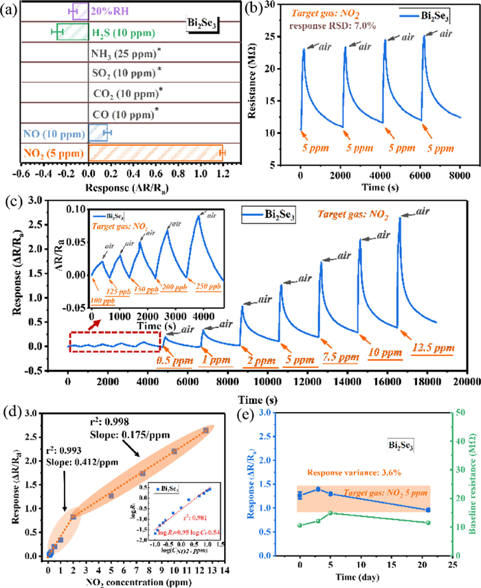
As for gas-sensing performance, firstly, several interference gases including water vapor, H2S, NH3, SO2, CO2, CO, and NO were selected to probe the cross-selectivity of the as-prepared Bi2Se3 sensors as shown in Fig. 2a. No obvious signals toward NH3, SO2, CO2, and CO occurred. As for humidity, H2S, and NO, all with higher concentration than NO2, the related response was much weaker than that toward NO2, indicating an excellent NO2 selectivity. Besides, the detailed time-resolved resistance curves toward various gases in Fig. S8 (Supporting information, namely, resistance declined for reducing water and H2S while rose for oxidizing NO and NO2) suggested the n-type semiconducting behavior of the as-prepared Bi2Se3 material. Moreover, the real-time resistance curves of the Bi2Se3 sensor on four successive exposures to 5 ppm NO2 were shown in Fig. 2b. The relative standard deviation (RSD) of the response over four cycles was 7.0%, verifying a favorable sensor repeatability. Furthermore, Fig. 2c exhibited the transient response of the Bi2Se3 sensor sequentially exposed to gradient NO2 from 100 ppb to 12.5 ppm. The response increased with NO2 concentration and the baseline drift was negligible. Inspiringly, the Bi2Se3 sensor displayed a noticeable response to ppb-level NO2 (Fig. 2c, inset), with the lowest experimental detection limit of 100 ppb. Subsequently, Fig. 2d directly revealed the response evolution over NO2 concentration. It was found that within the low NO2 concentration range (100 ppb-2 ppm), the response increased quickly (large sensitivity) due to abundant available adsorption sites on the Bi2Se3 surface. Nevertheless, the sensitivity faded within the large concentration range (2–12.5 ppm) ascribed into the gradual adsorption saturation. A nice linear dependence of the logarithm of the response on the logarithm of the NO2 concentration was obtained (R2 = 0.981) in the inset of Fig. 2d.

|
Download:
|
| Fig. 2. Gas sensing performance of the as-prepared Bi2Se3 sensor. (a) Selectivity (* note no response signal). (b) Dynamic resistance curve in cyclic tests toward 5 ppm NO2. (c) Real-time response toward different concentrations of NO2, the inset presented the real-time response at low concentration range (100–250 ppb NO2). (d) Relationship between response and NO2 concentration in linear and logarithmic scales (inset). (e) The response and baseline resistance drift within 21 days. | |
Further, the theoretical detection limit of NO2 was extracted as 6.3 ppb according to the IUPAC definition [42]. The Bi2Se3 sensor also possessed a short response time of 81 s toward 5 ppm NO2 and relatively long recovery time of 1143s at room temperature (Fig. S9 in Supporting information). Additionally, the Bi2Se3 sensor presented a slight response fluctuation (response variance: 3.6%) and baseline resistance drift within 21 days (Fig. 2e), and nearly identical sensing tendency toward 5 ppm NO2 at the 5th and 21st day (Fig. S10a and b in Supporting information), thereby proving a prominent long-term stability and reliability.
To explore the potential application capability, the humidity tolerance and the mechanical flexibility of the Bi2Se3 sensor were investigated. Firstly, the baseline resistance of the Bi2Se3 sensor was investigated under different RH in Fig. 3a. The slight decline of baseline resistance with increasing RH suggested the commendable inertness toward humidity, which could be attributed to the inherent hydrophobicity of Bi2Se3 material [43]. Fig. 3b exhibited the dynamic response curves toward 5 ppm NO2 under different RH conditions in detail. When RH increased from 0.3%RH (dry air) to 60%RH, the response was enhanced from 1.37 to 2.39 and recovery time was shortened from 1143s to 657 s (Fig. S11 in Supporting information), implying an inspiring prospect of the Bi2Se3 sensor for outdoor NO2 detection at room temperature [44]. As for the mechanical flexibility, no obvious alteration of the baseline resistance was observed with increased bend angle in Fig. 3c, indicating the excellent mechanical flexibility of the as-prepared Bi2Se3 sensor. Furthermore, the NO2-sensing performance of the Bi2Se3 sensor under different bend angles was explored in Fig. 3d. The sensing behaviors of the Bi2Se3 sensor under bend angles of 30°, 60°, and 90° were consistent with the unbent case. All these findings above demonstrated the fantastic application prospect of the flexible Bi2Se3 sensor especially in the field of wearable optoelectronic systems.

|
Download:
|
| Fig. 3. (a) Baseline resistance of Bi2Se3 sensor at different relative humidity. (b) The dynamic response curves of Bi2Se3 sensors toward 5 ppm NO2 at different relative humidity. (c) Baseline resistance of Bi2Se3 sensor at different bend angles. (d) The dynamic response curves of Bi2Se3 sensors toward 5 ppm NO2 at different bend angles. | |
Then, we summarized the sensing performance of the recently-reported NO2 sensor based on 2D materials in Table S1 (Supporting information). Apart from the unique application advantages for flexible electronics, the as-prepared Bi2Se3 sensor signified superior NO2-sensing performance in terms of higher response, lower operating temperature, and finer recognition resolution.
To reveal the NO2-sensing mechanism of Bi2Se3 material, the density functional theory (DFT) was performed to simulate the adsorption and charge transfer between NO2 gas and Bi2Se3 surface. Then, in order to achieve the gas molecular adsorption, we cleaved the surface from its bulk phase as shown in Fig. S12 (Supporting information). The adsorption energy and charge transfer between molecules and the basal surface of bismuth selenide were exhibited in Figs. 4a and b and Table S2 (Supporting information). It was found that the adsorption energy of NO2 reached −0.66 eV on the Bi2Se3 surface, which was several times larger than that of the rest molecules. Then, the side and top views of the favorable adsorption structures of various gases molecules were presented in Fig. 4c and Fig. S13 (Supporting information). Among all considered molecules, the adsorption distance of the NO2 was the nearest with the value reaching 2.55 Å for Bi2Se3. Besides, the most electron transfer from the thin film to the adsorbed molecule occurred after NO2 adsorption, suggesting that NO2 molecule was a strong electron acceptor. All these indicated the excellent NO2 selectivity of the Bi2Se3 thin film.

|
Download:
|
| Fig. 4. (a) The adsorption energy and (b) electron transfer of molecule adsorbed Bi2Se3. Side and top views favorable adsorption structure for (c) NO2, NO, H2O, and H2S molecules on Bi2Se3 basal surface. Purple, green, red, light blue, yellow and white spheres represent the Bi, Se, O, N, S, H atoms, respectively. | |
To clarify the electron transfer, we then calculated the charge density difference (CDD) to display the charge redistribution after the adsorption of gas molecules on Bi2Se3. As shown in Fig. S14 (Supporting information), the electrons were mainly accumulated around NO2 and NO molecules, while depleted from the surface Bi or Se atoms, indicating the significant electron transfer from Bi2Se3 to the adsorbed molecules. However, for H2O and H2S adsorption, the charge transferred in an opposite direction, which was consistent with above experimental results.
In addition to the basal surface adsorption mentioned above, we also simulated the NO2 adsorption on Bi2Se3 (100) edge. As shown in Fig. S15 (Supporting information), the adsorption energy of NO2 at edge sites was −0.82 eV, larger than that on the basal surface (−0.66 eV). This result confirmed that the exposure edges were crucial for further promoting the NO2 sensitivity of Bi2Se3 sensor, consistent with previous studies [14].
The sensing mechanism of the as-prepared Bi2Se3 nanoplates gas sensor toward NO2 can be classified into the typical charge transfer mechanism. When the as-prepared sensor was exposed to NO2, NO2 molecules were physisorbed directly on the surface of Bi2Se3 nanoplates and served as electron acceptors to obtain electrons from the conduction band of Bi2Se3 (Fig. S16 in Supporting information) [25,45]. For the n-type Bi2Se3, the loss of electrons resulted in a rise of material resistance. The process was presented in Eq. 1:

|
(1) |
In summary, we proposed one novel flexible gas sensor based on Bi2Se3 nanoplates for sensitive NO2 detection at room temperature for the first time, and explored the underlying sensing mechanism from the theoretical perspective. The as-prepared Bi2Se3 sensor exhibited favorable NO2-sensing performance in terms of selectivity, signal intensity, response speed, the detection limit, and humidity/flexibility-involved operation stability. It is foreseen that the as-prepared Bi2Se3 sensor probably paves a new avenue for the simple design of single-material based gas sensors without any additives or modifications.
Declaration of competing interestThe authors declare that they have no known competing financial interests or personal relationships that could have appeared to influence the work reported in this paper.
AcknowledgmentsThis work was partially supported by Fundamental and Frontier Research Project of Chongqing (Nos. cstc2019jcyj-msxmX0037 and cstc2020jcyj-msxmX1041), National Natural Science Foundation of China (Nos. 61704014 and 52175281), and Youth Innovation Promotion Association of CAS (No. 2021382).
Supplementary materialsSupplementary material associated with this article can be found, in the online version, at https://doi.org/10.1016/j.cclet.2022.107981.
| [1] |
R. Kumar, O. Al-Dossary, G. Kumar, A. Umar, Nanomicro. Lett. 7 (2015) 97-120. DOI:10.1007/s40820-014-0023-3 |
| [2] |
Y.J. Wang, D. Liu, J.B. Yin, et al., Chem. Commun. 56 (2020) 703-706. DOI:10.1039/c9cc09171h |
| [3] |
K. Wetchakun, T. Samerjai, N. Tamaekong, et al., Sens. Actuator. B: Chem. 160 (2011) 580-591. DOI:10.1016/j.snb.2011.08.032 |
| [4] |
Y.J. Wang, Y. Zhou, H. Ren, et al., Anal. Chem. 92 (2020) 11007-11017. DOI:10.1021/acs.analchem.9b05623 |
| [5] |
M. Chen, Z.H. Wang, D.M. Han, F.B. Gu, G.S. Guo, J. Phys. Chem. C 115 (2011) 12763-12773. DOI:10.1021/jp201816d |
| [6] |
X.X. Chen, Y.B. Shen, P.F. Zhou, et al., Sens. Actuator. B: Chem. 280 (2019) 151-161. DOI:10.1016/j.snb.2018.10.063 |
| [7] |
S.S. Shendage, V.L. Patil, S.A. Vanalakar, et al., Sens. Actuator. B: Chem. 240 (2017) 426-433. DOI:10.1016/j.snb.2016.08.177 |
| [8] |
P. Ding, D.S. Xu, N. Dong, et al., Chin. Chem. Lett. 31 (2020) 2050-2054. DOI:10.1016/j.cclet.2019.11.024 |
| [9] |
N. Luo, B. Zhang, D. Zhang, J.Q. Xu, Chin. Chem. Lett. 31 (2020) 2033-2036. DOI:10.1016/j.cclet.2020.01.002 |
| [10] |
X.R. Zhou, X.W. Cheng, Y.H. Zhu, et al., Chin. Chem. Lett. 29 (2018) 405-416. DOI:10.1016/j.cclet.2017.06.021 |
| [11] |
S. Liu, B. Yu, H. Zhang, T. Fei, T. Zhang, Sens. Actuator. B: Chem. 202 (2014) 272-278. DOI:10.1016/j.snb.2014.05.086 |
| [12] |
R. Kumar, X.H. Liu, J. Zhang, M. Kumar, Nanomicro. Lett. 12 (2020) 164. |
| [13] |
F. Wang, H.R. Zhong, Z.L. Chen, et al., Chin. Chem. Lett. 34 (2023) 107392. DOI:10.1016/j.cclet.2022.03.115 |
| [14] |
Y.S. Xu, J.Y. Xie, Y.F. Zhang, et al., J. Hazard. Mater. 411 (2021) 125120. DOI:10.1016/j.jhazmat.2021.125120 |
| [15] |
W. Zheng, X.H. Liu, J.Y. Xie, G.C. Lu, J. Zhang, Coord. Chem. Rev. 447 (2021) 214151. DOI:10.1016/j.ccr.2021.214151 |
| [16] |
J. Hu, M. Cheng, T. Wei, et al., Mater. Sci. Semicond. Process. 138 (2022) 106289. DOI:10.1016/j.mssp.2021.106289 |
| [17] |
D. Liu, Z.L. Tang, Z.T. Zhang, Sens. Actuator. B: Chem. 303 (2020) 127114. DOI:10.1016/j.snb.2019.127114 |
| [18] |
Y.J. Wang, Y. Zhou, Y.H. Wang, et al., Sens. Actuator. B: Chem. 349 (2021) 130770. DOI:10.1016/j.snb.2021.130770 |
| [19] |
C. Yang, J.Y. Xie, C.M. Lou, et al., Sens. Actuator. B: Chem. 333 (2021) 129571. DOI:10.1016/j.snb.2021.129571 |
| [20] |
Z.J. Yang, L. Jiang, J. Wang, et al., Sens. Actuator. B: Chem. 326 (2021) 128828. DOI:10.1016/j.snb.2020.128828 |
| [21] |
T.T. Liang, Z.F. Dai, Y.D. Liu, X. Zhang, H.B. Zeng, Sci. Bull. 66 (2021) 2471-2478. DOI:10.1016/j.scib.2021.07.007 |
| [22] |
F.B. Gu, R. Nie, D.M. Han, Z.H. Wang, Sens. Actuator. B: Chem. 219 (2015) 94-99. DOI:10.1016/j.snb.2015.04.119 |
| [23] |
S.Y. Cho, H.J. Koh, H.W. Yoo, H.T. Jung, Chem. Mater. 29 (2017) 7197-7205. DOI:10.1021/acs.chemmater.7b01353 |
| [24] |
R. Kumar, N. Goel, M. Kumar, ACS Sens. 2 (2017) 1744-1752. DOI:10.1021/acssensors.7b00731 |
| [25] |
J.Z. Ou, W.Y. Ge, B. Carey, et al., ACS Nano 9 (2015) 10313-10323. DOI:10.1021/acsnano.5b04343 |
| [26] |
L. Dong, X.F. Wang, P. Wang, H.G. Yu, J. Mater. Chem. C 10 (2022) 6402-6410. DOI:10.1039/d2tc00594h |
| [27] |
J.H. Kim, Y.J. Song, J.S. Rhyee, et al., Phys. Rev. B 87 (2013) 224305. DOI:10.1103/PhysRevB.87.224305 |
| [28] |
X.L. Qi, S.C. Zhang, Rev. Mod. Phys. 83 (2011) 1057-1110. DOI:10.1103/RevModPhys.83.1057 |
| [29] |
X.Y. Yang, S.S. Tian, R. Li, W. Wang, S.M. Zhou, Sens. Actuator. B: Chem. 241 (2017) 210-216. DOI:10.1016/j.snb.2016.10.074 |
| [30] |
C.J. Zhao, Y.H. Zou, Y. Chen, et al., Opt. Express 20 (2012) 27888-27895. DOI:10.1364/OE.20.027888 |
| [31] |
X.W. Chen, T. Wang, J. Shi, et al., Nanomicro Lett. 14 (2021) 8. |
| [32] |
R. Ahmed, Q.Y. Lin, Y. Xu, G. Zangari, Electrochim. Acta 299 (2019) 654-662. DOI:10.1016/j.electacta.2019.01.053 |
| [33] |
C.C. Dun, C.A. Hewitt, H.H. Huang, et al., ACS Appl. Mater. Interfaces 7 (2015) 7054-7059. DOI:10.1021/acsami.5b00514 |
| [34] |
M. Samanta, K. Biswas, Chem. Mater. 32 (2020) 8819-8826. DOI:10.1021/acs.chemmater.0c02129 |
| [35] |
T.T. Wang, J.Y. Liu, Y.L. Zhang, et al., J. Mater. Chem. A 10 (2022) 4306-4315. DOI:10.1039/d1ta10461f |
| [36] |
R.O. Ocaya, A.G. Al-Sehemi, A. Dere, F. Yakuphanoğlu, Sens. Actuator. A: Phys. 341 (2022) 113575. DOI:10.1016/j.sna.2022.113575 |
| [37] |
R.P. Ren, Z. Wang, J. Ren, et al., J. Mater. Sci. 54 (2018) 5918-5926. |
| [38] |
F. Zhou, Y.J. Zhao, W.C. Zhou, D.S. Tang, Appl. Sci. 8 (2018) 1794. DOI:10.3390/app8101794 |
| [39] |
L.M. Song, S.J. Zhang, C. Chen, X.Z. Hu, Q.W. Wei, Chem. Eng. J. 171 (2011) 1454-1457. DOI:10.1016/j.cej.2011.05.048 |
| [40] |
J.G. Analytis, J.H. Chu, Y.L. Chen, et al., Phys. Rev. B 81 (2010) 205407. DOI:10.1103/PhysRevB.81.205407 |
| [41] |
Y. Zhou, Y.J. Wang, Y.H. Wang, et al., Ceram. Int. 46 (2020) 16056-16061. DOI:10.1016/j.ceramint.2020.03.156 |
| [42] |
J. Li, Y.J. Lu, Q. Ye, et al., Nano Lett. 3 (2003) 929-933. DOI:10.1021/nl034220x |
| [43] |
P. Zhao, Y.F. Huang, Y.T. Shen, et al., Nanoscale 9 (2017) 3843-3849. DOI:10.1039/C7NR00521K |
| [44] |
R. Wagner, D. Schönauer-Kamin, R. Moos, J. Electrochem. Soc. 167 (2020) 167516. DOI:10.1149/1945-7111/abcb65 |
| [45] |
Z. Yang, C. Su, S.T. Wang, et al., Nanotechnology 31 (2020) 075501. DOI:10.1088/1361-6528/ab5271 |