b Fujian Engineering Research Center of Advanced Manufacturing Technology for Fine Chemicals, Fuzhou University, Fuzhou 350108, China;
c Fujian Science and Technology Innovation Laboratory for Optoelectronic Information of China, Fuzhou 350108, China
In recent years, with the increase of aerospace exploration missions from several countries, the study about the new electronic materials seems significant, because the working status of electronic devices will be greatly affected by the extreme environments (large range of temperature, high vacuum, and strong radiation) [1, 2]. Especially, in outer space, the working energy is mainly provided by solar panels, which demands urgently energy-saving devices, for example, low-power consumption memorizers [3, 4]. Another energy-saving mode is also important, i.e., the devices can silent at night but be turned on in daylight. Memorizer is an essential unit in aerospace electronics, the search for new high-performance memorizers with specific on-off performance and even visual stimuli responses (e.g., color changes) are highly desirable from the viewpoint of energy-saving [5, 6]. Currently, most of the attention was focused on the development of new memorizers working under normal conditions. Resistive random access memory (RRAM) devices are good candidates for the next-generation nonvolatile memory devices due to their simple structures, fast switching speeds, durability, high storage density, and low power consumption [7, 8]. Among them, hybrid organic-inorganic halide perovskite (HOIP)-based RRAM is fascinating owing to its high ON/OFF ratio, flexibility, multilevel property, and applicability to synapse devices [9, 10]. Especially, as effective photoactive components, HOIP has been used as photo-driven multilevel memories, which possess good multilevel memory behavior, multiple wavelengths accessible nonvolatility, and precise photo-responsibility of power/time-dependent illumination [11-13]. Particularly, great efforts have been paid to the optically driven photomemory (such as light-erasable nonvolatile memory) through a photoinduced recovery process [14-18]. Pulse-driven perovskite-based nonvolatile memory without holding electrical stress has been documented, which can greatly reduce energy consumption and accelerate read and write speeds [19]. But so far, the study about photo/thermal-triggered RRAM devices is still in its infancy, and only a POM-based memorizer with thermal-triggered mode working among 150–270 ℃ has been reported [11-13]. Compared to the conventional thermal/electrical-triggered modes, photon-programming can render a better energy-saving method, which can also simplify the device configuration and refrain the vertical leakage current in devices [20].
2D perovskites with greater Goldschmidt tolerance have illustrated versatile optoelectronic performances owing to the confinement of the electrons and holes in natural quantum wells defined by the perovskite layers [21, 22]. Especially, 〈110〉-oriented perovskites might have higher ion migration, better morphology, and higher charge transfer in the perovskite/substrate interface [23, 24]. So far, 〈110〉-oriented perovskites are very rare, most of which were constructed by using mixed ligands [25-27]. The searching for new 〈110〉-oriented perovskites using a single template will be significant due to their convenience in photoelectric device fabrication [28, 29]. Melamine (MLAI) and its co-crystals have been used as photo/thermal-responsive memory materials, whose three amine groups can provide strong hydrogen bonding to perovskite layers [30]. Furthermore, as a defect passivation material, melamine can be expected to enhance the solvent stability of perovskites by inhibiting hysteresis [31, 32]. In this study, we explore the structures of two new melamine-templated <110> -oriented perovskites and their application as unique visible light-triggered nonvolatile memorizers, whose status can be monitored by observable chromisms. This work will pave a new way for the development of next-generation energy-saving nonvolatile memorizers used in aerospace or military industries.
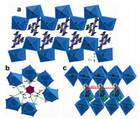
Two perovskites formulated as [(MLAI-H2)(PbX4)]n (X = Br (α-1), Cl (α-2)) are isostructures, which are made up of <110> -oriented corrugated perovskite-type inorganic sheets alternating with single (MLAI-H2)2+ organic template (Fig. 1a). The single-crystal structures before and after irradiation are also determined to correlate their following light-triggered performances, and the symbols of α and β correspond to their phases before and after irradiation. The PbX6 octahedra in this work are distorted deduced from Pb-X lengths (2.8714(9)~3.1824(10) Å for α-1, 2.7312(11)~3.0709(11) Å for α-2) and X-Pb-X angles (80.73(3)°~109.183(13)° for α-1, 79.06(3)°~109.183(13)° for α-2, Tables S2 and S3 in Supporting information). These also hint that the lone pair electrons of lead(Ⅱ) are stereochemically active [27]. The distorted degree is quantitatively estimated by Δd (Δd = (1/6) ∑[(d-d)/d]2) using Pb-X lengths [33]. Δd values of 1.78×10⁻³ (α-1) and 2.14×10⁻³ (α-2) demonstrate the high distortion of PbX6 octahedra. The PbX6 octahedra share neighboring corners (Br(1) for α-1, Cl(4) for α-2) along the c axis and opposite corners (Br(4) for α-1, Cl(2) for α-2) along the a axis to generate a zigzag perovskite sheets in the ac plane (Figs. S2 and S3 in Supporting information). The Pb-X-Pb angles defined by vertex-sharing halogen atoms are 163.08° (α-1) and 161.10° (α-2), which deviate greatly from the regular <110> -oriented perovskite sheet (180.00°) [25] and other contorted perovskite ones (144.23(2)°~171.85°) [28, 29]. Adjacent zigzag perovskite sheets are stabilized by the interleaved (MLAI-H2)2+ cations through hydrogen bonds and electrostatic interactions. The bis-protonization of ring N atoms is deduced from charge balances [30, 34]. In α-1, the N–H…X hydrogen bond lengths/angles are 2.46~2.70 Å/130~175° (for α-1) 2.29~2.78 Å/127°~175° (for α-2), suggesting the strong hydrogen bonds (Tables S4 and S5 in Supporting information, Fig. 1b) [30]. Based on these hydrogen bonds, the (MLAI-H2)2+ cations are anchored in the inter-layers, resulting in natural multi-quantum well-like structures (Fig. 1a and Fig. S3b) [35]. The distances among (MLAI-H2)2+ cations are 6.021(11) and 5.732(7) Å respectively, suggesting the absence of π…π stacking interactions (Fig. 1c). The perovskite layer-layer distances defined by the nearest X…X distance is 3.956(10) and 3.544(1) Å for α-1 and α-2 respectively.
|
Download:
|
| Fig. 1. (a) Crystal packing diagram showing the <110> -oriented corrugated (PbBr4)n2n− perovskite sheets in the ac plane and the positions of inserted (MLAI-H2)2+ cations. (b) Hydrogen bonds between perovskite sheets and (MLAI-H2)2+ cations. (c) The distances among (MLAI-H2)2+cations. | |
After irradiating, Δd value of 1.70×10⁻³ for β-1 and 2.16×10⁻³ for β-2 suggest that the distortion degree of PbBr6 octahedron is more sensitive to irradiation [36]. This trend can also be found in reduced Pb-X-Pb angles (162.59° for β-1 and 161.06° for β-2). Moreover, the perovskite sheets are compressed with shorter layer-layer distances in β-1 (3.900(2) Å), but those of β-2 increases slightly (3.550(2) Å). Finally, in both hybrids, the hydrogen bonds are strengthened after irradiating (Tables S4 and S5).
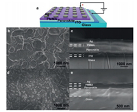
Considering that perovskite is easily degraded in ambient conditions, XRD measurements on these melamine-decorated perovskite powders and ITO-based films using the samples synthesized last year have been conducted, and the results show that the stabilities of they are reliable under environmental humidity (Fig. S4 in Supporting information). The memory devices with structures of ITO/[(MLAI-H2)(PbX4)]n/PMMA/Ag have been fabricated, whose vertical geometry is shown in Fig. 2a. Poly(methyl methacrylate) (PMMA) is dielectric without the resistive switching effect, which is often adopted as a charge blocking layer [37-39]. The surface morphologies and cross-section images were characterized by SEM (Figs. 2b–e). The thicknesses of the perovskite and the PMMA layers are about 1.14 µm/340 nm (for α-1) and 103.69 nm/82.14 nm (for α-2), respectively.
|
Download:
|
| Fig. 2. (a) Schematic illustration of ITO/perovskite/PMMA/Ag memory device; surface and cross-sectional SEM images: (b, c) ITO/α−1/PMMA/Ag device; (d, e) ITO/α−2/PMMA/Ag device. | |
Interestingly, these ITO/[(MLAI-H2)(PbX4)]n/PMMA/Ag devices can exhibit unique visible light-triggered binary nonvolatile memory performances. Before irradiating with visible light, these devices do not show obvious resistive switching behaviors in a voltage sweep of 0 V→ −5 V→ 0 V→ 5 V→ 0 V (Fig. 3a). But after 15 min (for α-1 based device, labeled as device-1) and 20 min (for α-2 based device, labeled as device-2) of exposure to the xenon lamp, the devices demonstrate the essential feature of bistable memory performances deduced from their typical hysteresis I-V curves (Figs. 3b and c), in which the currents jump between the high resistance states and the low resistance states upon applying the voltage sweeps [40]. It is worth mentioning that some I-V curves showing ternary memory behaviors can be detected on two irradiated devices, but the yields are low (10%), so we still describe them as binary memories. For the irradiated device-1 (Fig. 3b), it exhibits a high-resistance state (HRS, OFF state) when a voltage from −5.0 V to 0.0 V, then the current suddenly jumps to the low-resistance state (LRS, ON state) at 0.8 V (VSet). When the voltage sweeps back from −5.0 V to 0.0 V and then from 0 to −4.0 V, it remains in the LRS. Finally, the current can hop back to the HRS to complete this I-V loop when the voltage is −4.5 V (VReset). The higher VReset than the VSet suggests that the writing process is easier than erasing one, which is frequently observed in nonvolatile memories [5, 39]. Similar I-V characters can be observed in irradiated device-2, whose VSet and VReset are 1.063 and −4.97 V, respectively (Fig. 3c). Using a voltage of −0.1 V as the reading voltage, the ON/OFF ratios in a single cycle are estimated as 1.5 × 10⁴ (device-1) and 3.9 × 10³ (device-2), which are much higher than those based on methylamine perovskite without PMMA layers (such as Au/CH3NH3PbI3/ITO/PET, Ag/CH3NH3PbBr1.97Cl1.03/FTO/glass) [8, 41].

|
Download:
|
| Fig. 3. I–V curve ITO/perovskite/PMMA/Ag device before irradiating; (b) I–V curve of ITO/α−1/PMMA/Ag device after irradiating for 15 min; (c) I–V curve of ITO/α−2/PMMA/Ag device after irradiating for 20 min. | |
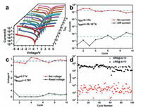
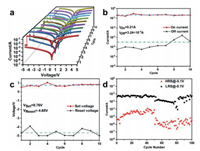
The resistive switching behaviors can be reproducible in the following cycles, which can be validated by their no obvious degradation of memory margins after 10 sweep cycles (Figs. 4a and 5a). The averaged ON/OFF ratio and VSet/VReset of two devices are 4.0 × 10³, 0.71/−4.70 V (for α-1 based device), and 0.65×10³, 0.76/−4.65 V (for α-2 based device) (Figs. 4b, c, 5b and c). Clearly, judging from the ON/OFF ratio and VSet/VReset values, the memory performance of Br-based <110> -oriented perovskite is better than that of Cl-based one. The memory stabilities can be further verified by the 100 sweeping cycles (Figs. 4d and 5d). After turning off the xenon lamp, the devices can maintain their electrical bistable behaviors for 48 h (for device-1) and 24 h (for device-2). Furthermore, when the xenon lamp is applied again, their resistive switches can be turned on again (Fig. 6).
|
Download:
|
| Fig. 4. (a) I-V characteristics of ITO/α−1/PMMA/Ag device after irradiating for 15 min with 10 cycles. (b) The current change of HRS and LRS with 10 cycles. (c) The change of VSet/VReset with 10 cycles. (d) Cycle endurance of the ITO/α−1/PMMA/Ag showing 100 cycles. | |
|
Download:
|
| Fig. 5. (a) I-V characteristics of ITO/α−2/PMMA/Ag device after irradiating for 20 min with 10 cycles. (b) The current change of HRS and LRS with 10 cycles. (c) The change of VSet/VReset with 10 cycles. (d) Cycle endurance of the ITO/α−2/PMMA/Ag showing 100 cycles. | |

|
Download:
|
| Fig. 6. (a) The persistence of memory devices after turning off the light and recovery when applying to irradiate again: (a) ITO/α−1/PMMA/Ag device; (b) ITO/α−2/PMMA/Ag device. | |
The light-triggered I-V curves have been fitted using Ohmic's and space charge limited conduction (SCLC) models to investigate their resistive switching mechanism (Figs. S5 and S6 in Supporting information) [42], [43]. In the low voltage region (0 → −2.72 V for device-1, 0 → −1.89 V for device-2) of the HRS, the I-V fitting follows the Ohm's law (I∝V, slope = 1.23 for device-1, slope = 1.01 for device-2), which can be explained as Schottky barrier rooting from the contact resistance in the PMMA/Ag interface (Figs. S5a and S6a). Afterward, in a higher negative voltage range (−2.72 → −5.00 V for device-1 and −1.92 → −5.00 V device-2), the relationship follows SCLC processes (I∝V2, slope = 2.82 for device-1, slope = 3.03 for device-2, Figs. S5b and S6b), during which the traps have been occupied gradually upon the injection of carriers. In this stage, the injected carriers are accommodating in the perovskite layer, consequently, an inverted internal electric field among carrier-trap couples will generate, which is contrary to the external electrical field and hinder the further carrier injection into the active layers [5, 6]. But with the increasing of the external voltages, more and more carriers are injected, leading to the resistive switching from the HRS to LRS at VSet. After transferring to LRS in the region of (−3.25 → 5.00 V for device-1 and −5.00 → 5.00 V for device-2), Ohmic conduction dominates these processes (Figs. S5c and S6c). The further back sweeping from 5.00 V to 0.85 V for device-1, the LRS jumps back to the HRS at the VReset, corresponding to the conduction mechanism switching into trap-unfilled SCLC (slope = 1.71, Fig. S5d). Finally, in the sweeping range of 0.85 → 0 V, the conduction mechanism transforms from the SCLC to the Ohmic (Fig. S5e). Similar behavior can be found in the sweeping range of 5.00 → 1.14 V and 1.06 → 0 V (Figs. S6d and e). In summary, SCLC and the Ohmic mechanisms govern the resistive switching performances in these <110> -oriented perovskite-based devices, which have been observed in relative devices [44-46].
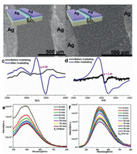
Moreover, the light-triggered binary resistive switching mechanisms of these ITO/perovskite/PMMA/Ag memory devices should also be clarified. Firstly, devices fabricated with mere perovskite and PMMA, i.e., ITO/perovskite/Ag and ITO/PMMA/Ag are both resistive switching silent before and after irradiating (Fig. S7 in Supporting information), hinting that their light-triggered memory behaviors stem from the synergism of two active moieties. The relatively high output currents in non-irradiated and ITO/PMMA/Ag devices might be led by excessive dark current based on ITO substrate [40]. Secondly, the metal filament penetration processes in these devices have been ruled out by lateral SEM images of Ag/perovskite/Ag model devices upon set/reset process, in which the formation of the filament between the two Ag electrodes could not be detected (Figs. 7a and b).
|
Download:
|
| Fig. 7. Lateral SEM images of the Ag/perovskite/Ag devices after set/reset process: (a) Ag/α−1/Ag; (b) Ag/α−2/Ag. EPR spectra before and after irradiating: (c) α−1; (d) α−2. Single-crystal fluorescent spectra under different irradiating times: (e) α−1; (f) α−2. | |
Therefore, the following possible scenario of the photo-triggered resistive switching process is proposed. In the relative perovskite-based memory devices, the resistive switching behaviors have mainly been attributed to the charge trapping in the perovskite active layers, in which the formation of an inverted internal electrical field is critical [6, 8, 41]. Especially, it has been pointed out that the <110> -preferred orientation in perovskites can result in reduced trap densities and longer carrier lifetimes [42]. Therefore, before irradiating, these PMMA-buffered high 〈110〉 texture perovskites with a large grain have fewer trap densities, as well as low leakage currents. Besides, their optical gaps seem large (3.22 and 3.82 eV, Fig. S8 in Supporting information). These electronic characters in their initial states lead to their resistive switching silence. After irradiating, the bulk perovskites can also absorb photons with energy higher than the value of the band-gap, consequently, electron-hole pairs can be produced in 2-D <110> -oriented perovskites, which can render the photovoltaic effect [13]. The photo-generated radicals can be validated by the EPR spectra of two perovskites, in which EPR signals are silent before irradiating but present after irradiating (Figs. 7c and d). Besides, meta-stable deep-level trap states will appear gradually after irradiating, which has been proved in CH3NH3PbI3 perovskite [46]. The light-activated traps can further be validated by irradiation-induced quenching fluorescence, in which the fluorescent densities decrease about 42.5% (irradiating for 15 min on α-1) and 36.7% (irradiating for 20 min on α-2) (Figs. 7e and f). These traps can serve as non-radiative recombination centers to enhance the non-radiative transfers, resulting in quenching fluorescence densities [36]. The bandgap narrowing upon light irradiating can also imply the formation of traps (Fig. S8), which can affect the current density in the SCLC process [46]. The more reduced bandgap in Br-based perovskite hints at its higher degree light-generated ionized dopant, corresponding to its better resistive switching behavior. The presence of photo-generated radicals indicates that the formations of light-activated traps are very slow because the traps can quench the radicals. In the light-irradiating ITO/perovskite/Ag devices upon applying an external voltage, electron-hole pairs generate firstly, which are further divided in the PMMA/[(MLAI-H2)(PbX4)]n perovskites interface by the external electric field. But this is not enough to turn on the resistive switching performances. Then light-activated traps appear after irradiating for 15 min, which can accommodate injected carriers to turn on the resistive switching performances. Therefore, the presence of light-activated traps in <110> -oriented [(MLAI-H2)(PbX4)]n perovskites is dominated in the light-triggered resistive switching behaviors. Together with photo-generated charge carriers and the injected hot carriers, the inverted internal electrical fields are established, based on which resistive switching behaviors are triggered. After removing the light resource, because no new light-activated traps generate, the existing ones will be annihilated in a long time [37]. Therefore, the memory performance can decay slowly and finally be turned off after 48 h (for device-1) and 24 h (for device-2). Importantly, as indicated by structural analysis, Br-containing perovskite is more sensitive to irradiation, which exhibits more distorted PbX6 octahedral, higher corrugated <110> -oriented perovskite sheets, and more condensed organic-inorganic packing. This trend is consistent with the observation that device-1 has a longer resistive switching duration after turning off the light (48 h). Therefore, these structural evolutions in 1 might be beneficial for the stabilization of light-activated traps, which lead to the better resistive switching behavior of device-1.
As illustrated by the UV–vis spectra (Fig. S9 in Supporting information), broad adsorption zones from 200 nm to 800 nm can be found, which contains the π–π* transitions of (MLAI-H2)2+ (below 400 nm) [30], <110> -oriented perovskites (at about 480 nm for 1 and 420 nm for 2) [47]. Especially, the relatively weak absorption in the visible zones stems from the organic-inorganic charge transfer (CT) led by hydrogen bonds [38]. With the elongating irradiating time, the absorption intensities increase, especially in the visible zones, which are consistent with their enhanced organic-inorganic interactions. Correspondingly, their colors change from colorless to pale yellow (especially for 1), indicating that the status of the devices can be monitored by their chromisms.
In summary, new <110> -oriented perovskites using single template melamine, i.e., [(MLAI-H2)(PbX4)]n (X = Br (α-1), Cl (α-2), MLAI=melamine) have been prepared and their structures upon irradiating of visible light have been investigated. They have been fabricated as nonvolatile memory devices with structures of ITO/[(MLAI-H2)(PbX4)]n/PMMA/Ag, which can exhibit unique visible light-triggered binary nonvolatile memory performances with the status being monitored by observable chromisms. Their light-triggered binary resistive switching mechanisms can be attributed to the presence of light-activated traps in <110> -oriented perovskites, which can be proved by their quenched fluorescence. X-ray single-crystal structural determinations on perovskites before and after irradiating also suggest that the more distorted PbX6 octahedra, higher corrugated <110> -oriented perovskite sheets, and more condensed organic-inorganic packing are beneficial for the stabilization of light-activated traps, which lead to the better resistive switching behavior of device-1. This work can pave a new avenue for the construction of novel energy-saving nonvolatile memorizers used in aerospace or military industries.
Declaration of competing interestThe authors declare that they have no known competing financial interests or personal relationships that could have appeared to influence the work reported in this paper.
AcknowledgmentsThis work was financially supported by the Natural Science Foundation of Fujian Province (Nos. 2021J02007, 2021J01553) and Fujian Science & Technology Innovation Laboratory for Optoelectronic Information of China (No. 2021ZR148).
Supplementary materialsSupplementary material associated with this article can be found, in the online version, at doi:10.1016/j.cclet.2022.04.062.
| [1] |
J.P. Randall, M.A.B. Meador, S.C. Jana, ACS Appl. Mater. Interfaces 3 (2011) 613-626. DOI:10.1021/am200007n |
| [2] |
K. Fayazbakhsh, A. Abedian, Adv. Space Res. 45 (2010) 741-749. DOI:10.1016/j.asr.2009.11.017 |
| [3] |
B.J. Choi, A.C. Torrezan, J.P. Strachan, et al., Adv. Funct. Mater. 26 (2016) 5290-5296. DOI:10.1002/adfm.201600680 |
| [4] |
X. Wu, H. Yu, J. Cao, AIP Adv. 10 (2020) 085202. DOI:10.1063/1.5130914 |
| [5] |
B. Chen, Y.R. Huang, K.Y. Song, et al., Chem. Mater. 33 (2021) 2178-2186. DOI:10.1021/acs.chemmater.1c00090 |
| [6] |
Y.R. Huang, X.L. Lin, B. Chen, et al., Angew. Chem. Int. Ed. 60 (2021) 16911-16916. DOI:10.1002/anie.202104333 |
| [7] |
J.J. Yang, D.B. Strukov, D.R. Stewart, Nat. Nanotechnol. 8 (2013) 13-24. DOI:10.1038/nnano.2012.240 |
| [8] |
C. Gu, J.S. Lee, ACS Nano 10 (2016) 5413-5418. DOI:10.1021/acsnano.6b01643 |
| [9] |
B. Hwang, J.S. Lee, Adv. Mater. 29 (2017) 1701048. DOI:10.1002/adma.201701048 |
| [10] |
A. Younis, C.H. Lin, X. Guan, et al., Adv. Mater. 33 (2021) 2005000. DOI:10.1002/adma.202005000 |
| [11] |
J.Y. Chen, Y.C. Chiu, Y.T. Li, et al., Adv. Mater. 29 (2017) 1702217. DOI:10.1002/adma.201702217 |
| [12] |
Y. Wang, Z. Lv, Q. Liao, et al., Adv. Mater. 30 (2018) 1800327. DOI:10.1002/adma.201800327 |
| [13] |
T. Paul, P.K. Sarkar, S. Maiti, et al., ACS Appl. Electron. Mater. 2 (2020) 3667-3677. DOI:10.1021/acsaelm.0c00719 |
| [14] |
C.H. Chen, Y. Wang, H. Tatsumi, et al., Adv. Funct. Mater. 29 (2019) 1902991. DOI:10.1002/adfm.201902991 |
| [15] |
Y.J. Jeong, D.J. Yun, S.H. Kim, et al., ACS Appl. Mater. Interfaces 9 (2017) 11759-11769. DOI:10.1021/acsami.7b02365 |
| [16] |
Y.J. Jeong, D.J. Yun, S.H. Noh, et al., ACS Nano 12 (2018) 7701-7709. DOI:10.1021/acsnano.8b01413 |
| [17] |
Y.H. Chang, C.W. Ku, Y.H. Zhang, et al., Adv. Funct. Mater. 30 (2020) 2000764. DOI:10.1002/adfm.202000764 |
| [18] |
M.Y. Liao, Y.C. Chiang, C.H. Chen, et al., ACS Appl. Mater. Interfaces 12 (2020) 36398-36408. DOI:10.1021/acsami.0c10587 |
| [19] |
S.J. Chang, S.Y. Chen, P.W. Chen, et al., ACS Appl. Mater. Interfaces 11 (2019) 33803-33810. DOI:10.1021/acsami.9b08766 |
| [20] |
C. Ríos, M. Stegmaier, P. Hosseini, et al., Nat. Photonics 9 (2015) 725-732. DOI:10.1038/nphoton.2015.182 |
| [21] |
L. Pedesseau, D. Sapori, B. Traore, et al., ACS Nano 10 (2016) 9776-9786. DOI:10.1021/acsnano.6b05944 |
| [22] |
M. Yuan, L.N. Quan, R. Comin, et al., Nat. Nanotechnol. 11 (2016) 872-877. DOI:10.1038/nnano.2016.110 |
| [23] |
J. Yin, D. Cortecchia, A. Krishna, et al., J. Phys. Chem. Lett. 6 (2015) 1396-1402. DOI:10.1021/acs.jpclett.5b00431 |
| [24] |
Y.C. Shih, Y.B. Lan, C.S. Li, et al., Small 13 (2017) 1604305. DOI:10.1002/smll.201604305 |
| [25] |
D.B. Mitzi, S. Wang, C.A. Feild, et al., Science 267 (1995) 1473-1476. DOI:10.1126/science.267.5203.1473 |
| [26] |
S. Wang, D.B. Mitzi, C.A. Feild, et al., J. Am. Chem. Soc. 117 (1995) 5297-5302. DOI:10.1021/ja00124a012 |
| [27] |
Y. Wang, W. Li, T. Zhang, et al., Small Methods 4 (2020) 1900511. DOI:10.1002/smtd.201900511 |
| [28] |
Y. Li, G. Zheng, J. Lin, Eur. J. Inorg. Chem. 2008 (2008) 1689-1692. |
| [29] |
Y.Y. Li, C.K. Lin, G.L. Zheng, et al., Chem. Mater. 18 (2006) 3463-3469. DOI:10.1021/cm060714u |
| [30] |
Q. Liu, L. Zhao, W. Wu, et al., J. Mater. Chem. C 8 (2020) 3258-3267. DOI:10.1039/C9TC05843E |
| [31] |
S.G. Kim, J. Chen, J.Y. Seo, et al., ACS Appl. Mater. Interfaces 10 (2018) 25372-25383. DOI:10.1021/acsami.8b06616 |
| [32] |
F. Yang, M.A. Kamarudin, D. Hirotani, et al., Sol. RRL 3 (2019) 1800275. DOI:10.1002/solr.201800275 |
| [33] |
J.A. Alonso, M.J. Martínez-Lope, M.T. Casais, et al., Inorg. Chem. 39 (2000) 917-923. DOI:10.1021/ic990921e |
| [34] |
B. Hamdi, R. Zouari, A. Ben Salah, Superlattices Microstruct 123 (2018) 97-110. DOI:10.1016/j.spmi.2018.04.025 |
| [35] |
T. Ishihara, J. Takahashi, T. Goto, Phys. Rev. B 42 (1990) 11099-11107. DOI:10.1103/PhysRevB.42.11099 |
| [36] |
W. Nie, J.C. Blancon, A.J. Neukirch, et al., Nat. Commun. 7 (2016) 11574. DOI:10.1038/ncomms11574 |
| [37] |
G. Ding, Y. Wang, G. Zhang, et al., Adv. Funct. Mater. 29 (2019) 1806637. DOI:10.1002/adfm.201806637 |
| [38] |
Y. He, Y.R. Huang, Y.L. Li, et al., Inorg. Chem. 58 (2019) 13862-13880. DOI:10.1021/acs.inorgchem.9b01740 |
| [39] |
W. Wu, X.L. Lin, Q. Liu, et al., Inorg. Chem. Front. 7 (2020) 1451-1466. DOI:10.1039/C9QI01672D |
| [40] |
X. Chen, P. Huang, X. Zhu, et al., Nanoscale Horiz. 4 (2019) 697-704. DOI:10.1039/C8NH00366A |
| [41] |
C. Muthu, S. Agarwal, A. Vijayan, et al., Adv. Mater. Interfaces 3 (2016) 1600092. DOI:10.1002/admi.201600092 |
| [42] |
L. Liang, K. Li, C. Xiao, et al., J. Am. Chem. Soc. 137 (2015) 3102-3108. DOI:10.1021/jacs.5b00021 |
| [43] |
X. Zhang, J. Xu, X. Zhang, et al., Mater. Sci. Semicond. Process 57 (2017) 105-109. DOI:10.1016/j.mssp.2016.09.031 |
| [44] |
H.T. Wu, Y.F. Chen, C.F. Shih, et al., Thin Solid Films 660 (2018) 320-327. DOI:10.1016/j.tsf.2018.06.032 |
| [45] |
J. Lian, Q. Wang, Y. Yuan, et al., J. Mater. Chem. A 3 (2015) 9146-9151. DOI:10.1039/C5TA01595B |
| [46] |
V.M. Le Corre, E.A. Duijnstee, O. El Tambouli, et al., ACS Energy Lett. 6 (2021) 1087-1094. DOI:10.1021/acsenergylett.0c02599 |
| [47] |
S. Sourisseau, N. Louvain, W. Bi, et al., Chem. Mater. 19 (2007) 600-607. DOI:10.1021/cm062380e |
 2023, Vol. 34

