 2022, Vol. 33


b School of Electronic Science and Engineering, Xiamen University, Xiamen 361005, China;
c Future Display Institute of Xiamen, Xiamen 361005, China
Solution-processed organic-inorganic metal-halide perovskites have received considerable attention due to their excellent optoelectronic properties. Remarkable progress has been achieved in perovskite light-emitting diodes (LEDs) by optimizing materials and device structures, with external quantum efficiencies (EQEs) now over 20% [1-4], which are close to that of organic LEDs [5, 6]. To realize commercial perovskite LEDs, simplifying the fabrication process is important.
Typically, a perovskite LED consists of an emitting active layer in between the electron transport layer (ETL) and the hole transport layer (HTL), which play the roles of transporting electron/hole transport and blocking the opposite carrier [7-9]. To realize good carrier injection and recombination, this device structure raises high requirement for the design of transport layers [10, 11]. Alternatively, multiple-transport-layer structure is often adopted [12-14]. Moreover, because the crystallization of perovskite can be easily affected by the underneath layer, an interface modification layer is often included [15-17]. This makes the fabrication of perovskite LED becoming more complicated. Recently, a strategy of using insulator to substitute hole transport layer has been introduced to simplify the structure of perovskite LEDs. Shi et al. used an ultrathin LiF film to replace the conventional PEDOT: PSS/PVK layers, which can induce charge injection through tunneling effect and suppress the charge quenching at the interface [18]. Similarly, MgO was introduced to fabricate hole-injection-layer-free perovskite LEDs [19]. However, these devices still need the additional insulation layer.
Here, we demonstrate a new strategy to fabricate hole-transport-layer-free LEDs based on quasi-two-dimensional (quasi-2D) layered perovskite. The quasi-2D perovskite can naturally form multiple-quantum-well (MQW) structure with organic layer as potential barrier and inorganic layer as potential well [20-24]. Typically, it consists of MQW layered perovskites with various bandgaps which are determined by the number of PbX4 in each quantum well (QW) [25]. The MQW structure can be simply controlled by changing the precursor compositions and deposition processes, etc. [23, 26, 27]. We find that the QW with large bandgap can assemble near the ITO anode and work as electron-blocking layer, which impedes the leakage current in devices, thereby leading to efficient perovskite LEDs.
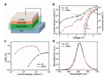
The device has a structure of ITO/perovskite (~100 nm)/1,3,5-tri(m-pyridin-3-ylphenyl) benzene (TmPyPB, 45 nm)/lithium fluoride (LiF, 1.2 nm)/aluminum (Al, 100 nm) (Fig. 1a). The MQW perovskite layer was prepared onto ITO glass substrates through spin-coating at 4000 rpm for 45 s from a precursor solution of propylamine hydrobromide (PABr), formamidinium bromide (FABr) and lead bromide (PbBr2) (PABr: FABr: PbBr2 = 0.4:0.9:1) dissolved in dimethylformamide (DMF) (18 wt%), followed by annealing at 60 ℃ for 15 min. For the three-dimensional (3D) perovskite, it was prepared from a precursor solution of FABr and PbBr2 with a molar ratio of 1.3:1. Subsequently, the ETL layer (TmPyPB) and electrode (LiF/Al) were sequentially thermally evaporated at a pressure of 2 × 10⁻⁴ Pa.

|
Download:
|
| Fig. 1. (a) Schematic illustration of perovskite LED device structure. (b) Dependence of the current density and luminance on the driving voltage. (c) Dependence of the EQE on the current density. (d) EL spectra. | |
LED devices were measured in a N2-filled glovebox by using an integrating sphere system [25, 28]. The measurements of device stability were carried out by using a LST800 system, Nanjing Ouyi Optoelectronics Technology. Grazing-incidence wide-angle X-ray scattering (GIWAXS) images were collected at the SAXS/WAXS beamline at the Australian Synchrotron. Scanning electron microscope (SEM) images and atomic force microscopy (AFM) images were obtained by a JEOL5 JSM-7800F SEM and a Park XE7 atomic force microscope, respectively. X-ray diffraction (XRD) data were collected by using a Bruker D8 Advance. The excitation-intensity-dependent photoluminescence quantum efficiencies (PLQEs) were measured through a method combining CW laser, optical fiber, spectrometer and integrating sphere (PLQE-LD CP001, Nanjing Ouyi Optoelectronics Technology) [29]. Ionization photoelectron spectrometer (IPS) spectra were obtained by an IPS-4, Nanjing Sunny Tech. Ltd. All films were prepared on ITO glass or quartz substrates.
Current density-voltage characteristics of perovskite LEDs show that the MQW perovskite LED has a much smaller leakage current than that of 3D perovskite LED without HTL (Fig. 1b). Moreover, the MQW perovskite LED reaches a peak EQE of 9.0% (Fig. 1c), which is similar as the device with PEDOT: PSS layer (Fig. S1 in Supporting information), representing the record EQE of HTL-free perovskite LEDs (Table S1 in Supporting information). The device has a maximum luminance up to ~2700 cd/m2, with a stable electroluminescence (EL) peak at 528 nm (Figs. 1b and d, Fig. S2 in Supporting information). In contrast, the EQE of 3D perovskite LED without HTL is only 1.4%. Moreover, the MQW perovskite LED shows better stability than the 3D device (Fig. S3 in Supporting information), which should be mainly due to the suppression of ion migration through the inclusion of large organic cation in quasi-2D layered perovskite [30]. The EQE of perovskite LED is the product of internal quantum efficiency (IQE) and outcoupling efficiency (ηout).
|
(1) |
where γ is the fraction of formed emissive excitons (~100%), ηcap is the charge capture efficiency (depending on the device structure and morphology of perovskite film), ηout and photoluminescence quantum efficiency (PLQE) are determined by the optical structure of device and the emission efficiency of perovskite film respectively. Therefore, this enhanced performance of MQW perovskite LED should stem from the improved PLQE or ηcap.
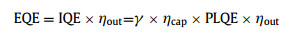
Fig. 2a shows that the MQW perovskite film has a maximum PLQE of ~40%, while that of the 3D perovskite is only ~20%. This enhanced PL efficiency can be attributed to the suppressed trap-induced nonradiative recombination through efficient energy transfer from large bandgap QW to small bandgap component [25]. This result suggests that besides the two-fold enhanced PL efficiency of MQW perovskite, the charge capture efficiency should also play an important role in the improved EQE of HTL-free LEDs.

|
Download:
|
| Fig. 2. (a) Excitation-intensity-dependent PLQE. SEM images of (b) 3D and (c) MQW perovskite film. The scale bars represent 1 µm. | |
To reveal the origin of the higher charge capture efficiency in the MQW perovskite LED, we compared the morphology of 3D and MQW perovskite films. It shows that all the perovskite films have uniform and compact morphology (Figs. 2b and c, Figs. S4 and S5 in Supporting information), albeit there are some variations in grain size, which is consistent with the XRD data (Fig. S6 in Supporting information). This indicates that the improved charge capture efficiency can not be ascribed to the difference in film coverage.
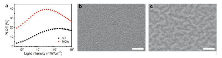
We then characterized the structure of MQW perovskite film by performing GIWAXS measurements as a function of incidence angle (α), which can provide the structure of film in different depths. For α < 0.2°, the X-rays can penetrate only the top 10 nm of the film, while for α = 0.2°−0.5°, the measurement can give the whole information of film [31]. Fig. 3a shows that for α = 0.15°, there is a peak at q = 10.5 nm−1, which is close to the (100) crystal plane of 3D FAPbBr3 perovskite [32, 33], suggesting the surface component is 3D-like FAPbBr3 perovskite. Moreover, the Debye-Scherrer ring indicates the random orientation of the surface perovskite. As X-rays penetrate into the whole film (α ≥ 0.22°) (Figs. 3b and c), the signals from 2D perovskites were observed, showing peaks at q = 3.5 nm−1 and 7.0 nm−1 at 45° azimuth angle [31]. This result suggests that in the MQW perovskite film, the 2D layered perovskites locate under the 3D-like perovskite and stack along 45° (Fig. 3d).

|
Download:
|
| Fig. 3. (a-c) GIWAXS images of MQW perovskite film with incidence angles of 0.15°, 0.30° and 0.50°, respectively. (d) Schematic illustration of the MQW perovskite film structure. | |
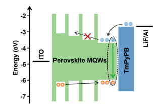
Next, the IPS measurements show that the large bandgap 2D perovskite has similar valence band, but shallower conduction band compared to the small bandgap perovskite (Figs. S7 and S8 in Supporting information). Fig. 4 shows that this large bandgap 2D perovskite naturally forms a barrier for electron transporting to the anode, thus impedes the leakage current (Fig. 1b), enhancing the charge capture efficiency.

|
Download:
|
| Fig. 4. Flat-band energy level diagram of the MQW LED. The energy level values of perovskites were obtained by IPS and optical measurements. | |
In conclusion, we have demonstrated a facile approach to achieve efficient HTL-free LED device by using MQW layered perovskite. The unique structure of MQW perovskite can effectively block the electrons to the anode interface in LEDs, which plays the role as electron blocking layer. Using the simple structure of Anode/Perovskite/ETL/Cathode, we achieved MQW perovskite LED with significantly improved performance (> 6 times) compared to 3D perovskite LED. We believe that the performance of HTL-free MQW perovskite LEDs can be further boosted by improving the PLQE of perovskite film. Our work provides a new strategy for fabricating HTL-free perovskite LEDs, which is attractive for low-cost, large-area lighting and display applications.
Declaration of competing interestThe authors declare that they have no known competing financial interests or personal relationships that could have appeared to influence the work reported in this paper.
AcknowledgmentsThis work is financially supported by the Major Research Plan of the National Natural Science Foundation of China (No. 91733302), the National Natural Science Foundation of China (Nos. 61875084, 61922041, 61961160733, 61974126, 51902273), the National Science Fund for Distinguished Young Scholars (No. 61725502), the Natural Science Foundation of Jiangsu Province, China (No. BK20180085), the Major Program of Natural Science Research of Jiangsu Higher Education Institutions of China (No. 19KJA520004), the Joint Research Funds of the Department of Science & Technology of Shaanxi Province and NPU (No. 2020GXLH-Z-024), the Synergetic Innovation Center for Organic Electronics and Information Displays, a part of this research was undertaken on the SAXS/WAXS beamline at the Australian Synchrotron.
Supplementary materialsSupplementary material associated with this article can be found, in the online version, at doi:10.1016/j.cclet.2021.06.084.
| [1] |
Y. Cao, N. Wang, H. Tian, et al., Nature 562 (2018) 249-253. DOI:10.1038/s41586-018-0576-2 |
| [2] |
W. Xu, Q. Hu, S. Bai, et al., Nat. Photonics 13 (2019) 418-424. DOI:10.1038/s41566-019-0390-x |
| [3] |
Y. Dong, Y.K. Wang, F. Yuan, et al., Nat. Nanotechnol. 15 (2020) 668-674. DOI:10.1038/s41565-020-0714-5 |
| [4] |
Y.H. Kim, S. Kim, A. Kakekhani, et al., Nat. Photonics 15 (2021) 148-155. DOI:10.1038/s41566-020-00732-4 |
| [5] |
M. Sassi, N. Buccheri, M. Rooney, et al., Sci. Rep. 6 (2016) 34096. DOI:10.1038/srep34096 |
| [6] |
Z. Wei, K. Zhang, C.K. Kim, et al., Chin. Chem. Lett. 32 (2021) 493-496. DOI:10.1016/j.cclet.2020.05.005 |
| [7] |
Z.K. Tan, R.S. Moghaddam, M.L. Lai, et al., Nat. Nanotechnol. 9 (2014) 687-692. DOI:10.1038/nnano.2014.149 |
| [8] |
B.R. Sutherland, E.H. Sargent, Nat. Photonics 10 (2016) 295-302. DOI:10.1038/nphoton.2016.62 |
| [9] |
G.L. Yang, H.Z. Zhong, Chin. Chem. Lett. 27 (2016) 1124-1130. DOI:10.1016/j.cclet.2016.06.047 |
| [10] |
T. Liu, Y. Jiang, M. Qin, et al., Nat. Commun. 10 (2019) 878. DOI:10.1038/s41467-019-08843-5 |
| [11] |
S. Tan, X. Wu, Y. Zheng, et al., Chin. Chem. Lett. 30 (2019) 1951-1954. DOI:10.1016/j.cclet.2019.08.003 |
| [12] |
J. Si, Y. Liu, Z. He, et al., ACS Nano 11 (2017) 11100-11107. DOI:10.1021/acsnano.7b05191 |
| [13] |
T. Chiba, Y. Hayashi, H. Ebe, et al., Nat. Photonics 12 (2018) 681-687. DOI:10.1038/s41566-018-0260-y |
| [14] |
Y. Hassan, J.H. Park, M.L. Crawford, et al., Nature 591 (2021) 72-77. DOI:10.1038/s41586-021-03217-8 |
| [15] |
J. Wang, N. Wang, Y. Jin, et al., Adv. Mater. 27 (2015) 2311-2316. DOI:10.1002/adma.201405217 |
| [16] |
N. Wang, L. Cheng, J. Si, et al., Appl. Phys. Lett. 108 (2016) 141102. DOI:10.1063/1.4945330 |
| [17] |
L. Zhang, X. Yang, Q. Jiang, et al., Nat. Commun. 8 (2017) 15640. DOI:10.1038/ncomms15640 |
| [18] |
Y. Shi, W. Wu, H. Dong, et al., Adv. Mater. 30 (2018) 1800251. DOI:10.1002/adma.201800251 |
| [19] |
Z. Shi, L. Lei, Y. Li, et al., ACS Appl. Mater. Interfaces 10 (2018) 32289-32297. DOI:10.1021/acsami.8b07048 |
| [20] |
J. Calabrese, N.L. Jones, R.L. Harlow, et al., J. Am. Chem. Soc. 113 (1991) 2328-2330. DOI:10.1021/ja00006a076 |
| [21] |
D.B. Mitzi, K. Chondroudis, C.R. Kagan, IBM J. Res. Dev. 45 (2001) 29-45. DOI:10.1147/rd.451.0029 |
| [22] |
P. Tyagi, S.M. Arveson, W.A. Tisdale, J. Phys. Chem. Lett. 6 (2015) 1911-1916. DOI:10.1021/acs.jpclett.5b00664 |
| [23] |
L. Cheng, T. Jiang, Y. Cao, et al., Adv. Mater. 32 (2020) 1904163. DOI:10.1002/adma.201904163 |
| [24] |
L. Cheng, Y. Cao, R. Ge, et al., Chin. Chem. Lett. 28 (2017) 29-31. DOI:10.1016/j.cclet.2016.07.001 |
| [25] |
N. Wang, L. Cheng, R. Ge, et al., Nat. Photonics 10 (2016) 699-704. DOI:10.1038/nphoton.2016.185 |
| [26] |
Y. Sun, L. Zhang, N. Wang, et al., Npj Flex. Electron. 2 (2018) 12. DOI:10.1038/s41528-018-0026-0 |
| [27] |
L. Zhu, D. Liu, J. Wang, N. Wang, J. Phys. Chem. Lett. 11 (2020) 8502-8510. DOI:10.1021/acs.jpclett.0c02476 |
| [28] |
M. Anaya, B.P. Rand, R.J. Holmes, et al., Nat. Photonics 13 (2019) 818-821. DOI:10.1038/s41566-019-0543-y |
| [29] |
J.C. de Mello, H.F. Wittmann, R.H. Friend, Adv. Mater. 9 (1997) 230-232. DOI:10.1002/adma.19970090308 |
| [30] |
C. Li, N. Wang, A. Guerrero, Y. Zhong, et al., J. Phys. Chem. Lett. 10 (2019) 6857-6864. DOI:10.1021/acs.jpclett.9b02467 |
| [31] |
R. Yang, R. Li, Y. Cao, et al., Adv. Mater. 30 (2018) 1804771. DOI:10.1002/adma.201804771 |
| [32] |
S. Kumar, J. Jagielski, N. Kallikounis, et al., Nano Lett. 17 (2017) 5277-5284. DOI:10.1021/acs.nanolett.7b01544 |
| [33] |
A. Greco, A. Hinderhofer, M.I. Dar, et al., J. Phys. Chem. Lett. 9 (2018) 6750-6754. DOI:10.1021/acs.jpclett.8b02916 |