 2022, Vol. 33


b University of Chinese Academy of Sciences, Beijing 10049, China;
c School of Physical Education, China University of Geosciences, Wuhan 430074, China
Microfluidic devices have been widely harnessed in various fields, such as drug screening [1], protein renaturation [2], DNA sequencing [3], cell analysis [4-6], chemical synthesis [7] and others [8]. Among various types of microdevices, PDMS-based device is the most popular one utilized in biochemical analysis due to its high precision, low cost, good optical performance and biocompatibility [9]. Current PDMS devices are often manufactured based on soft lithography, where a photoresist mold is obtained by photolithography for prototyping [10, 11]. Since the photoresist mold tightly attaches to a substrate (often a silicon wafer), it allows multiple repeated PDMS pouring and peeling off and contributes to the stability of the following on-chip experiments. Unfortunately, common photolithography requires highly-skilled persons, multiple expensive instruments and complex fabrication procedures performed in a high-maintenance cleanroom (Fig. S1 in Supporting information). These special requirements hinder the accessibility of PDMS devices to the research community, especially for those from general biochemical laboratories without fabrication facilities and experiences [12].
To simplify the fabrication procedure of microfluidic devices, many methods have been proposed [13]. For example, computer numerical control (CNC) micromachining and laser cutter engraving have been widely used to directly fabricate PMMA [14] or even PDMS devices [15], but the generated microchannels often present as a V-shape cross section due to the uneven distribution of laser energy in these relatively stiff materials [16]. Laser cutter was also applied to generate microchannels on double-sided adhesive tape that was integrated with a plastic slab and a glass slide to form a microdevice [17]. Three-dimensional (3D) printing has also been used to produce devices with scaffolding materials such as acrylonitrile butadiene styrene (ABS) and polyvinyl alcohol (PVA), but the process of dissolving the scaffold could swell the PDMS matrix and the resulted microchannel resolution is relatively low [18]. Liquid molding is another rapid prototyping method for PDMS device manufacture [19, 20]. This strategy is free from expensive instruments for photolithography, but it still needs a premade mask and extra care during PMDS pouring process to avoid water mold disruption [13]. Table S1 (Supporting information) shows a brief summarization of currently used methods for rapid microfluidic device fabrication.
Herein, we demonstrate a laser cutter-based fabrication strategy to rapidly generate a tape frame for making positive photoresist-based mold for rapid prototyping of PDMS devices. Since cutting tape requires minimal laser energy, a relatively high-resolution mold (~100 µm) is obtained within 5 minutes by a simple heating step, exempting photolithography steps. As tape thickness and layer number are of flexible selectivity, it is easy to generate microchannels with different heights. This method allows the generation of photoresist molds like traditional photolithography, but eliminates the requirement of clean room facilities and complex procedures (Table S1). The fabricated PDMS devices showed good performance in the proof-of-concept experiments such as chemical reaction monitoring and cell culture. We anticipate this fast, low-cost and flexible fabrication strategy to be widely used in common biochemical laboratories.
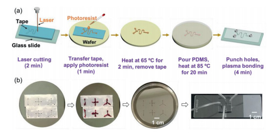
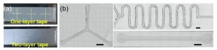
As shown in Fig. 1a, the adhesive tape is attached onto a glass slide to carry out the laser cutting. The laser power and scanning speed were optimized to be 1 W and 2.5 cm/s, respectively. After laser ablation (Fig. 1a), the tape is transferred to a clean silicon wafer. Then a drop of positive photoresist (SPR 220-7) is applied onto the ablated area of the tape and the extra photoresist is scraped away from the tape with a cover glass. After a simple heating at 65 ℃ for 2 min, the photoresist-based male mold is obtained after removing the tape. PDMS devices are manufactured by prototyping the mold. The total fabrication time is within 30 min. The experimental fabrication processes are shown in Fig. 1b. Since the tape is a thin soft material, it requires minimal energy to cut through and produces little debris and smooth channels. Due to this characteristic of adhesive tape, it is possible to generate relatively higher resolution microstructures when comparing with other hard materials such as PMMA [21, 22]. As shown in Fig. 2, one- or two-layer tape can be processed rapidly and the finally obtained patterns achieved a resolution of ~100 µm. The mold height can be easily controlled by changing tape layers (Fig. 2a and Fig. S2 in Supporting information) or using tapes with different thicknesses. This strategy also enables high-throughput fabrication of multiple micropatterns when attaching the tape strips on a large PMMA sheet (Fig. S3 in Supporting information).

|
Download:
|
| Fig. 1. Laser-cutter based photolithography-free method procedures for prototyping of PDMS devices. (a) Scheme. (b) Experimental processes. | |

|
Download:
|
| Fig. 2. Micropatterns generated based on laser cutting. (a) One- and two-layer tape processed after laser ablation. (b) Micrograph of the PDMS channels after prototyping the photoresist mold. Scale bar, 300 µm. | |
Photoresist-based mold endures high temperature and attaches tightly on the substrate, which allows multiple times of PDMS replication with high fidelity [23]. As described above, our strategy only requires two simple steps to get a photoresist-based mold within 5 min. However, current soft lithography needs laborious procedures to fabricate a mold. For example, to obtain a negative photoresist-based (e.g., SU-8) mold, multiple steps are necessary, including spin-coating, pre-bake, UV-exposure (requiring a mask printed in advance), post-bake, developing and hard bake (Fig. S1). These experimental steps, normally performed in a clean room, require the use of many hazardous chemical substances and expensive instruments. It takes about 4 h to finish these procedures. Though typical positive photoresist-based (e.g., SPR220) mold does not necessarily require hard bake, it is essential to perform the other procedures including photolithography. It is known that the UV-exposed area of positive photoresist is dissolved during developing, while the non-exposed area remains on the substrate. In contrast to the traditional way, our strategy directly generates a positive photoresist-based mold by using the laser ablated tape as a constraint frame, which greatly simplifies the fabrication procedure and avoids photolithography and hazardous chemicals.
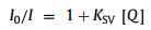
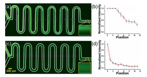
Next, we moved to test the performance of the PDMS devices fabricated by using our strategy. As a proof-of-concept experiment for studying chemical reaction, a Y-shape micromixer with a serpentine mixing channel was designed, fabricated and tested (Fig. 2a). Quenching reaction of KI to fluorescein is often used to evaluate the mixing performance of a micromixer [24, 25]. The two solutions were injected into the micromixer from the two inlets. According to Stern-Volmer equation (Eq. 1),
|
(1) |
where I0 and I are the fluorescence intensities without and with quenchers respectively, KSV is Stern-Volmer constant (9.608 ± 0.273), [Q] is the concentration of iodide, 70% fluorescence quenching can be achieved if 0.5 mol/L KI is completely mixed with the fluorescein solution. When the flow rate was set as 0.1 mL/h, the fluorescence did not achieve an even distribution at the outlet (Figs. 3a and b). When the flow rate was decreased to 0.03 mL/h, the two solutions had sufficient time to diffuse and achieved a complete mixing (the final normalized fluorescence was ~0.3) at the outlet, as shown in Figs. 3c and d.

|
Download:
|
| Fig. 3. Results of fluorescence quenching experiment. Fluorescence image under (a) 0.1 and (c) 0.03 mL/h, respectively. Normalized fluorescence intensity at different positions along the microchannel under (b) 0.1 and (d) 0.03 mL/h, respectively. The positions of 0–12 were marked by the purple lines shown in (a) and (c). | |
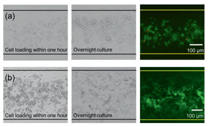
Furthermore, we tested the biocompatibility of the fabricated PDMS device. Two types of cells (HeLa and U87) with different adhesive behaviors were loaded into the device with a straight channel (Fig. 4). HeLa cells are relatively low adhesive, and the cells showed short protrusions after overnight culture. For the U87 (human glioblastoma cell line) cells with a high adhesion ability, long protrusions were monitored. The live/dead staining with calcein and PI demonstrated that both cells showed high viability in the devices, though the image of HeLa cells displayed several red spots that could be cell debris. In a two-day on-chip culture, HeLa cells also demonstrated good status, as shown in the bright-field image in Fig. S4 (Supporting information). These proof-of-concept experiments displayed that the PDMS devices obtained with our strategy have great biocompatibility for cell culture.

|
Download:
|
| Fig. 4. Micrograph showing on-chip cell culture and staining. (a) HeLa cells. (b) U87 cells. | |
In summary, we proposed a new strategy to fabricate microfluidic PDMS devices within 30 min. Notably, a photoresist-based mold can be obtained in 5 min without photolithography. This method shows a fabrication resolution around 100 µm based on current settings, but better resolution could be achieved by finely tunning the laser power or using an updated laser cutter with higher-resolution lens, which may further promote this technique to be widely used in more refined experiments such as single cell analysis. The surface roughness of the microchannels (e.g., the side wall) could also be improved if the cutting resolution is improved, though current devices already satisfies the requirement of common biochemical reactions (Fig. 2b). Two typical biochemical experiments including quenching reaction and cell culture/staining were demonstrated to confirm the device performance. These proof-of-concept studies show that our strategy could serve as an efficient method for rapid prototyping of PDMS devices and holds great potential to be widely used in general biochemical libraries.
Declaration of competing interestThe authors declare that they have no known competing financial interests or personal relationships that could have appeared to influence the work reported in this paper.
AcknowledgmentsWe thank Shunji Li and Dr. Peng Chen for their help in the laser cutter operation. We gratefully acknowledge the financial support from the National Natural Science Foundation of China (Nos. 21904139, 22074152, 21735007), Chinese Academy of Sciences (Nos. Y9Y1041001, YJKYYQ20170026).
Supplementary materialsSupplementary material associated with this article can be found, in the online version, at doi:10.1016/j.cclet.2021.07.045.
| [1] |
B. Schuster, M. Junkin, S.S. Kashaf, et al., Nat. Commun. 11 (2020) 5271. DOI:10.1038/s41467-020-19058-4 |
| [2] |
M. He, J. Novak, B.A. Julian, A.E. Herr, J. Am. Chem. Soc. 133 (2011) 19610-19613. DOI:10.1021/ja207963f |
| [3] |
T. Hoshino, R. Nakao, H. Doi, T. Minamoto, Sci. Rep. 11 (2021) 4372. DOI:10.1038/s41598-021-83318-6 |
| [4] |
Y. Li, J.D. Motschman, S.T. Kelly, B.B. Yellen, Anal. Chem. 92 (2020) 2794-2801. DOI:10.1021/acs.analchem.9b05099 |
| [5] |
Y. Li, P. Zhang, T. Li, et al., Sens. Actuators B: Chem. 308 (2020) 127749. DOI:10.1016/j.snb.2020.127749 |
| [6] |
Q. Zhang, S. Feng, W. Li, et al., Angew. Chem. Int. Ed. 60 (2021) 8483-8487. DOI:10.1002/anie.202016171 |
| [7] |
L. Rao, B. Cai, L.L. Bu, et al., ACS Nano 11 (2017) 3496-3505. DOI:10.1021/acsnano.7b00133 |
| [8] |
Z. Wu, Y. Zheng, L. Lin, et al., Angew. Chem. Int. Ed. 59 (2020) 2225-2229. DOI:10.1002/anie.201911252 |
| [9] |
A. Mata, A.J. Fleischman, S. Roy, Biomed. Microdevices 7 (2005) 281-293. DOI:10.1007/s10544-005-6070-2 |
| [10] |
J.P. Rolland, E.C. Hagberg, G.M. Denison, K.R. Carter, J.M. De Simone, Angew. Chem. Int. Ed. 43 (2004) 5796-5799. DOI:10.1002/anie.200461122 |
| [11] |
D.C. Duffy, J.C. McDonald, O.J.A. Schueller, G.M. Whitesides, Anal. Chem. 70 (1998) 4974-4984. DOI:10.1021/ac980656z |
| [12] |
B. Gale, A. Jafek, C. Lambert, et al., Inventions 3 (2018) 60. DOI:10.3390/inventions3030060 |
| [13] |
G.G. Morbioli, N.C. Speller, A.M. Stockton, Anal. Chim. Acta 1135 (2020) 150-174. DOI:10.1016/j.aca.2020.09.013 |
| [14] |
Y. Ren, S. Ray, Y. Liu, Sci. Rep. 9 (2019) 4824. DOI:10.1038/s41598-019-41208-y |
| [15] |
M. Li, S. Li, J. Wu, et al., Microfluid. Nanofluid. 12 (2011) 751-760. |
| [16] |
M.M. Islam, A. Loewen, P.B. Allen, Sci. Rep. 8 (2018) 8763. DOI:10.1038/s41598-018-27037-5 |
| [17] |
D. Patko, Z. Mártonfalvi, B. Kovacs, et al., Sens. Actuators B: Chem. 196 (2014) 352-356. DOI:10.1016/j.snb.2014.01.107 |
| [18] |
M. Saadat, M. Taylor, A. Hughes, A.M. Hajiyavand, Adv. Mech. Eng. 12 (2020) 1-12. |
| [19] |
Y. Lu, B. Lin, J. Qin, Anal. Chem. 83 (2011) 1830-1835. DOI:10.1021/ac102577n |
| [20] |
S.Q. Yan, S.T. Wang, Z.J. Hao, et al., Biofabrication 13 (2021) 03005. |
| [21] |
D.A. Bartholomeusz, R.W. Boutte, J. Microelectromech. Syst. 14 (2005) 1364-1374. DOI:10.1109/JMEMS.2005.859087 |
| [22] |
R. Samuel, C.M. Thacker, A.V. Maricq, B.K. Gale, J. Micromech. Microeng. 24 (2014) 105007. DOI:10.1088/0960-1317/24/10/105007 |
| [23] |
Y. Xia, G.M. Whitesides, Angew. Chem. Int. Ed. 37 (1998) 550-575. DOI:10.1002/(SICI)1521-3773(19980316)37:5<550::AID-ANIE550>3.0.CO;2-G |
| [24] |
Y. Li, C. Liu, X. Feng, Y. Xu, B.F. Liu, Anal. Chem. 86 (2014) 4333-4339. DOI:10.1021/ac500112d |
| [25] |
R. Hu, C. Liu, J. Xuan, et al., Sens. Actuators B: Chem. 293 (2019) 312-320. DOI:10.1016/j.snb.2019.05.026 |