 2022, Vol. 33


b Institute of Molecular Materials and Devices, Fudan University, Shanghai 200433, China;
c Institute of Chemistry, Chinese Academy of Sciences, Beijing 100190, China
Organic single crystals (OSCs) have gained great interest in the last decades, owing to their potential applications in wearable electronics such as transparent circuits and flexible displays [1-8]. The main subtractive manufacturing strategies of OSCs are vapor deposition and solution-based deposition [9-11]. The vapor process has been hindered by costly equipment and harsh processing conditions. Many researchers focus on the solution process, which corresponds to the central demands for industrialization, low cost, rapidity and user-friendliness. The solution-based deposition includes drop-casting, solution shearing, spin-coating and so on [12-17]. These processes hardly pattern the OSCs in a controllable manner to achieve the requirements of multifunctional organic electronics [18]. In recent years, some addictive manufacturing methods are developed to pattern the OSCs, such as inkjet printing [10, 19-21], contact evaporation printing [1], capillary-bridge lithography and window printing [22-26], which achieve high accuracy in patterning the OSCs. Nevertheless, the subtractive manufacturing of OSCs, as an essential process in the manufacture of organic electronics, is far behind.
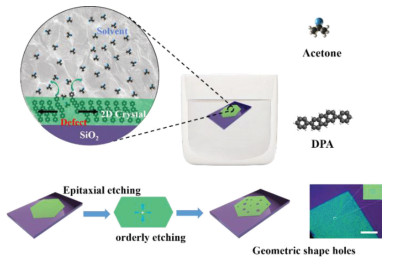
The subtractive manufacturing, especially the etching, has been widely used in the semiconductor industry for patterning diverse inorganic semiconductors [27-32]. The OSCs are a kind of molecular crystal assembled via van der Waals interaction which is much weaker than the covalent bonds. The OSCs are too vulnerable to afford the damages from the subtractive manufacture, leading to dramatic degradation of the performance after the process. Till now, it is still a challenge to pattern OSCs in micron-scale without damage of the crystallinity through a simple process. Here, we develop an epitaxial etching strategy for controllably subtractive manufacturing of OSCs. It clips 2, 6-diphenyl anthracene (DPA) crystals into microribbon arrays. After etching, the resulting materials maintain high crystallinity with mobility around 89% value of the original crystals, showing its great potential for manufacturing high performance devices based on OSCs.
The epitaxial etching is a kind of wet etching which starts from defects and boundaries and epitaxial etching along with some specific crystal axis. As shown in Fig. 1, the two-dimensional (2D) DPA crystals is epitaxial etched from the defects by etchant and forms regular parallelogram holes (Fig. 1, Figs. S1a and S2 in Supporting information). These holes, just like crystals, are born from a core named defect. Then they epitaxially grow along with the specific crystal axis. Finally, they all become the same regular shape and have the same orientation.

|
Download:
|
| Fig. 1. Schematic illustration of the epitaxial etching. | |
The epitaxial etching has high controllability, which is dominated by a thermodynamic process. The etching is reversible since the DPA has a poor solubility in acetone. After the epitaxial etching, the crystals maintain high crystallinity. As a result, the DPA crystals are bright in the dark field of polar optical microscope (POM, shown in Fig. S1a), revealing the high crystallinity after etching. In order to explore whether epitaxial etching only occurs in wet etching, a thermal etching method is employed to etch DPA crystals. The thermal etching is usually used in crystal study [33]. DPA crystals are put on hotplate and etched by heating. The results are shown in Fig. S1b (Supporting information), the thermal etching of the DPA crystals is a disorder process. The etching starts from the substrate and induces internal defects and cracks. Many irregular holes appear after the etching. Different with the wet epitaxial etching, the crystal cannot maintain a stable or metastable state at high temperature, thus the etching process is accompanied with the generation of defects and cracks.
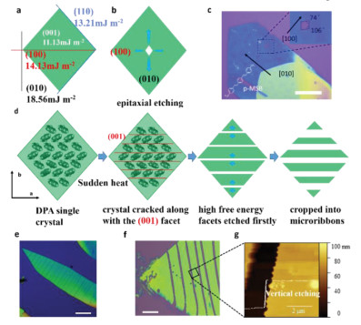
The epitaxial etching starts from the grain boundaries or defects, then extends outwards or inwards along with specific crystal facets. According to the Gibbs-Wulff theorem, the stable shape of a crystal should obey the energy minimum law in a thermodynamical equilibrium [34]. It means that the total of every crystal facet area weighted by its surface free energy should be minimalized [35]. Therefore, the molecules prefer to deposit on the crystal facet which has higher surface free energy to achieve the lowest total surface free energy. Vice versa, the facets with higher surface free energy should be etched more quickly than other facets. The specific facets depend on the crystal facet free energy. Fig. 2a shows the surface free energy of 1, 4-bis(4-methylstyryl)benzene (p-MSB, a kind of typical organic semiconductor crystal) crystals. The crystal facet free energies of (110), (100), (010) and (001) crystal facet of p-MSB are 13.21 mJ/m2, 14.30 mJ/m2, 18.56 mJ/m2 and 11.13 mJ/m2, respectively [36]. Owing to the large facet free energy of (010) and (100), the etching along [010] and [100] directions are faster than other facets (Fig. 2b). Thus, the epitaxially etched holes have a parallelogrammatic shape with diagonals at [100] and [010] directions (Fig. 2c). The angles between hole edges are 74° and 106°, which are the included angles of (110) and (110), (110) and (110), respectively. Other facets, such as (001), are etched much slowly, which seems to be protected by "the sacrificial facets".

|
Download:
|
| Fig. 2. (a) The crystal facet surface free energy of the p-MSB crystal. (b) Schematic illustration of the epitaxial etching of the p-MSB crystal. The (100) and (010) facets are etched. (c) OM image of epitaxially etched p-MSB crystal. Parallelogrammatic holes form with diagonals at [100] and [010] directions. The angles between the edges are 74° and 106°. (d) Schematic illustration of the preparation of the DPA micro-ribbon arrays. (e, f) OM images and (g) AFM images of the DPA micro-ribbon. The scale bars are 200 m (e), 20 m (f). | |
By the epitaxial etching, we cut the organic crystals into micro-ribbon arrays almost without damaging the rest parts. The crystal surface free energy can be estimated from the morphology of the DPA crystals. The DPA crystals are parallelogram sheets crystallized in chlorobenzene or toluene solution (Fig. S3a in Supporting information). Referring to the Gibbs–Curie–Wulff law, the (010), (010), (001) and (001) facets at four corners of the parallelogram have the highest free energy as well as the fastest etching speed in the solvent. The largest crystal facets, which are (100) and (100), have the lowest free energy and etching speed. As shown in Fig. S3b (Supporting information), the holes of epitaxially etched DPA are parallelogram, and their diagonals are at [100] and [010] directions. According to the Gibbs–Curie–Wulff law, DPA crystals prefer a two-dimensional (2D) growth mode and the largest facet should be (001) in thermodynamical equilibrium. More importantly, the (001) facet has the lowest free energy, thus it is most difficult to be etched, preventing the epitaxial etching from damaging the crystallinity of the DPA crystals.
Compared with the epitaxial etching, the DPA crystals after the thermal etching are more disordered. After a short time of the thermal etching, the DPA crystals will crack from the most fragile crystal facets. These cracks are too small to be detected by optical microscope (OM, Fig. S4 in Supporting information). Scanning electron microscope (SEM) image clearly shows some parallel cracks along [001] zone axis of the DPA crystals. These cracks are believed to be caused by the thermal expansion coefficient differences between substrates and crystals [37]. According to the crystal structure (Fig. 2d), the DPA molecules have small van-der-Waals interactions in the (001) facets. The anisotropic van-der-Waals interactions also induce an anisotropic thermal expansion coefficient. Thus, the DPA crystals are weakly compacted at [001] direction apt to be broken down along this direction. Based on this phenomenon, we prepare high quality DPA micro-ribbon arrays by the epitaxial etching.
The crystal micro-ribbon arrays could be applied in flexible device. Because the gaps between ribbons can leak the strength of deformation, and the ribbon structure can also increase the Young's modulus of them. These facts can all make the crystals harder to crack in flexible environment. The formation of DPA micro-ribbon arrays includes both the thermal etching and the epitaxial etching (Fig. 2d). Firstly, the DPA crystals grow on Si/SiO2 through the drop-casting method. Then, the substrates are heated on a hot plate for 1 min at 100 ℃. Some parallel cracks are obtained in these crystals after heating. The cracked crystals are dipped in acetone etchants in few seconds after cooling them down at ambient temperature. These crystal cracks form new grain boundaries which are firstly etched in epitaxial etching. The etchant starts etching the crystals from these new boundaries aiming to achieve a minimum surface free energy. Finally, the crystals are cut into micro-ribbon arrays along with a specific direction, [001] crystal zone axis (Fig. 2e). In addition, the (001) facets have the largest surface free energy. Thus, the cracked crystals are cut into micro-ribbon arrays with barely damaging other facets, especially the in-plane facets (100). The acetone slowly etches the DPA crystal. Therefore, the crystal is controllably etched and maintains high crystallinity as well. The POM images (Fig. S5 in Supporting information) show the resulting materials are still bright in the dark field of polar optical microscope (POM), indicating that the micro-ribbon arrays have the high crystallinity after the epitaxial etching. The width of gaps is governed by the etching time (Fig. S6 in Supporting information). In the first 5 s, the DPA crystals are etched from the cracks. With the increase of the etched time, gaps grow bigger. The width of the gaps can be adjusted by tuning the etching time. It is worth mentioning that during the epitaxial etching process, the (100) crystal facet is not obviously etched. Figs. 2f and g show the gaps morphology. The etched edges have serrations about tens of nanometers wide, and the gaps are sharply vertical. These characteristics reveal that the etched edge has a high quality.
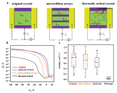
To study the influence of the epitaxial etching to the electrical properties, top contact bottom gate organic field-effect transistors (OFETs) are fabricated by the DPA crystal on octadecyltrichlorosilane (OTS) modified SiO2/Si substrates. The structure of the device is shown in Fig. 3a. 100 nm Au films are transferred by gold-layer sticking technique [38] on original, thermally etched, the epitaxially etched DPA crystals or DPA micro-ribbon arrays, respectively, as source and drain electrodes. The epitaxial etching scarcely has impact towards charge transmission of the resulting crystals (Fig. 3a). However, the thermally etched DPA have many defects and cracks which hinder the charge transport (Fig. 3c). The transfer curves are shown in Fig. 3b. The DPA OFETs exhibit typical p-type characteristics. The on/off ratios of the original DPA single crystals (red line), the epitaxially etched DPA crystals (blue line), and the micro-ribbon arrays (green line) are around 107, while the thermally etched DPA crystals have a value around 2 orders of magnitude lower than the others. The average hole mobility of over 30 OFETs of the DPA micro-ribbon arrays (Fig. 3c) is 0.72 cm2 V-1 s-1, which is 89% of the DPA original crystals (0.81 cm2 V-1 s-1). In contrast, the average hole mobilities of the OFETs made of epitaxially etched and the thermally etched DPA crystals are 0.63 cm2 V-1 s-1 and 0.02 cm2 V-1 s-1, respectively.

|
Download:
|
| Fig. 3. (a) Schematic illustration of top-contact bottom-gate OFETs made of pristine DPA crystals, DPA micro-ribbon arrays and thermally etched DPA crystals. (b) Transfer curve of pristine DPA (red), epitaxially etched DPA (blue), DPA micro-ribbon arrays (orange) and thermally etched DPA crystal (black). (c) Hole mobility distribution of pristine DPA crystals (red), mocro-ribbons arrays (orange), epitaxially etched crystals (blue) and thermally etched crystals (black). The average hole mobilities are 0.81 cm2 V-1 s-1, 0.72 cm2 V-1 s-1, 0.63 cm2 V-1 s-1 and 0.02 cm2 V-1 s-1, respectively. | |
The electrical characteristics of the micro-ribbon arrays are scarcely degraded after the epitaxial etching. Although the efficient charge transport of DPA crystals is along [010] (b axis), the charge transport along [001] does not have much difference. The hole mobility along [001] is about 0.7 times of that along [010] [22]. It means that the micro-ribbon arrays are still qualified for efficient carrier transport, although some charge transport channels have been broken off due to the cutting process. The DPA micro-ribbon arrays have nearly the same electrical performance as the pristine DPA single crystals, indicating that the subtractive manufacturing by the epitaxial etching has a neglectable influence on the device performance.
In this work, we develop an epitaxial etching strategy to subtractively manufacture the OSCs, which maintains high crystallinity as well as the electrical performance. The epitaxial etching obeys the Gibbs–Curie–Wulff laws, and the etching speed depends on the crystal surface free energy of each facet. As an example, we prepare highly crystalline micro-ribbon arrays of OSCs with 89% mobility of the original crystals. This work solves a longstanding challenge of the subtractive manufacturing of OSCs. Further development of the epitaxial etching method along with subtractive manufacturing technologies will be expected to fabricate complicated organic logic circuits and functional systems in a highly controllable manner.
Declaration of competing interestThe authors declare no competing financial interest.
AcknowledgmentsThis work was supported by the National Key R & D Program of China (No. 2018YFA0703200), the National Natural Science Foundation of China (Nos. 51773041, 61890940), Shanghai Committee of Science and Technology in China (No. 18ZR1404900), the Strategic Priority Research Program of the Chinese Academy of Sciences (No. XDB30000000), State Key Laboratory of Molecular Engineering of Polymers and Fudan University.
Appendix Supplementary materialsSupplementary material associated with this article can be found, in the online version, at doi:10.1016/j.cclet.2021.06.030.
| [1] |
A. Briseno, S. Mannsfeld, M. Ling, et al., Nature 444 (2006) 913-917. DOI:10.1038/nature05427 |
| [2] |
J. Liu, H. Zhang, H. Dong, et al., Nat. Commun. 6 (2015) 10032. DOI:10.1038/ncomms10032 |
| [3] |
C. Wang, H. Dong, W. Hu, Y. Liu, D. Zhu, Chem. Rev. 112 (2012) 2208-2267. DOI:10.1021/cr100380z |
| [4] |
J. Mei, Y. Diao, A.L. Appleton, L. Fang, Z. Bao, J. Am. Chem. Soc. 135 (2013) 6724-6746. DOI:10.1021/ja400881n |
| [5] |
J. Kwon, Y. Takeda, R. Shiwaku, et al., Nat. Commun. 10 (2019) 54. DOI:10.1038/s41467-018-07904-5 |
| [6] |
M. He, Y. Zhao, Y. Liu, D. Wei, Chin. Chem. Lett. 31 (2020) 826-830. DOI:10.1016/j.cclet.2019.06.003 |
| [7] |
X. Ma, Y. Yi, Chin. Chem. Lett. 31 (2020) 797-800. DOI:10.1016/j.cclet.2019.05.024 |
| [8] |
P. He, H. Zhang, C. Xu, et al., Chin. Chem. Lett. 30 (2019) 903-905. DOI:10.1016/j.cclet.2019.02.012 |
| [9] |
C. Reese, Z. Bao, Mat. Today 10 (2007) 20-27. DOI:10.1016/S1369-7021(07)70016-0 |
| [10] |
H. Minemawari, T. Yamada, H. Matsui, et al., Nature 475 (2011) 364-367. DOI:10.1038/nature10313 |
| [11] |
M. He, X. Chen, D. Liu, D. Wei, Chin. Chem. Lett. 30 (2019) 961-965. DOI:10.1016/j.cclet.2019.01.008 |
| [12] |
L. Jiang, H. Dong, W. Hu, J. Mater. Chem. 20 (2010) 4994-5007. DOI:10.1039/b925875b |
| [13] |
Y. Liu, X. Zhao, B. Cai, et al., Nanoscale 6 (2014) 1323-1328. DOI:10.1039/C3NR05680E |
| [14] |
G. Giri, E. Verploegen, S.C. Mannsfeld, et al., Nature 480 (2011) 504-508. DOI:10.1038/nature10683 |
| [15] |
Y. Diao, B.C. Tee, G. Giri, et al., Nat. Mater. 12 (2013) 665-671. DOI:10.1038/nmat3650 |
| [16] |
Y. Yuan, G. Giri, A.L. Ayzner, et al., Nat. Commun. 5 (2014) 3005. DOI:10.1038/ncomms4005 |
| [17] |
M.R. Niazi, R. Li, E.Q. Li, et al., Nat. Commun. 6 (2015) 8598. DOI:10.1038/ncomms9598 |
| [18] |
K.C. Dickey, S. Subramanian, J.E. Anthony, et al., Appl. Phys. Lett. 90 (2007) 244103. DOI:10.1063/1.2748841 |
| [19] |
M. Yoneya, H. Minemawari, T. Yamada, T. Hasegawa, J. Phys. Chem. C 121 (2017) 8796-8803. DOI:10.1021/acs.jpcc.7b02143 |
| [20] |
S.Y. Cho, J.M. Ko, J. Lim, J.Y. Lee, C. Lee, J. Mater. Chem. C 1 (2013) 914-923. DOI:10.1039/C2TC00360K |
| [21] |
A.C. Ihnen, A.M. Petrock, T. Chou, et al., Appl. Surf. Sci. 258 (2011) 827-833. DOI:10.1016/j.apsusc.2011.08.125 |
| [22] |
J. Feng, X. Jiang, X. Yan, et al., Adv. Mater. 29 (2017) 1603652. DOI:10.1002/adma.201603652 |
| [23] |
H. Gao, J. Feng, B. Zhang, et al., Adv. Funct. Mater. 27 (2017) 1701347. DOI:10.1002/adfm.201701347 |
| [24] |
J. Feng, Q. Song, B. Zhang, et al., Adv. Mater. 29 (2017) 1703143. DOI:10.1002/adma.201703143 |
| [25] |
Z. Dai, Q. Ou, C. Wang, et al., J. Mater. Chem. C 7 (2019) 5954-5961. DOI:10.1039/c9tc01104h |
| [26] |
S. Duan, T. Wang, B. Geng, et al., Adv. Mater. 32 (2020) 1908388. DOI:10.1002/adma.201908388 |
| [27] |
W.R. Harshbarger, R.A. Porter, T.A. Miller, P. Norton, Appl. Spectrosc. 31 (1977) 201-207. DOI:10.1366/000370277774463698 |
| [28] |
M. Kodama, M. Sugimoto, E. Hayashi, et al., Appl. Phys. Expr. 1 (2008) 021104. DOI:10.1143/APEX.1.021104 |
| [29] |
C. Youtsey, I. Adesida, L.T. Romano, G. Bulman, Appl. Phys. Lett. 72 (1998) 560-562. DOI:10.1063/1.120758 |
| [30] |
C. Youtsey, L.T. Romano, I. Adesida, Appl. Phys. Lett. 73 (1998) 797-799. DOI:10.1063/1.122005 |
| [31] |
C. Youtsey, I. Adesida, G. Bulman, Appl. Phys. Lett. 71 (1997) 2151-2153. DOI:10.1063/1.119365 |
| [32] |
C. Youtsey, G. Bulman, I. Adesida, J. Electron. Mater. 27 (1998) 282-287. DOI:10.1007/s11664-998-0400-0 |
| [33] |
I. Swiderski, J. Cryst. Growth 16 (1972) 1-9. DOI:10.1016/0022-0248(72)90079-6 |
| [34] |
C. Herring, Angew. Chem. 65 (1953) 34-35. DOI:10.1002/ange.19530650106 |
| [35] |
M. Cao, C. Zhang, Z. Cai, et al., Nat. Commun. 10 (2019) 756. DOI:10.1038/s41467-019-08573-8 |
| [36] |
R. Li, X. Zhang, H. Dong, et al., Adv. Mater. 28 (2016) 1697-1702. DOI:10.1002/adma.201504370 |
| [37] |
H. Li, J. Wu, K. Takahashi, et al., J. Am. Chem. Soc. 141 (2019) 10007-10015. DOI:10.1021/jacs.9b03819 |
| [38] |
Q. Tang, L. Jiang, Y. Tong, et al., Adv. Mater. 20 (2008) 2947-2951. DOI:10.1002/adma.200800669 |