 2022, Vol. 33


b Department of Applied Physics, The Hong Kong Polytechnic University, Hong Kong, China;
c School of Physics, Southeast University, Nanjing 211189, China;
d College of Jincheng, Nanjing University of Aeronautics and Astronautics, Nanjing 211156, China;
e School of Physics and Technology, Nanjing Normal University, Nanjing 210023, China;
f Department of Chemistry, National University of Singapore, Singapore 117543, Singapore;
g Institute of Materials Research and Engineering, Agency for Science, Technology and Research (A*STAR), Innovis 138634, Singapore;
h Global Innovative Centre for Advanced Nanomaterials, College of Engineering, Science and Environment, The University of Newcastle, Newcastle NSW 2308, Australia
Black phosphorus (BP) has attracted strong interests beyond graphene due to its high carrier mobility and layer-dependent bandgap (~0.3 eV for bulk and ~2.0 eV for monolayer) [1-3]. Few-layer BP has been considered as an excellent platform for phototransistors due to light-driven thermoelectric, photobolometric and photovoltaic processes [4]. Previously, few-layer BP photodetectors have been demonstrated to exhibit fast and wide-spectrum responses with a photo-responsivity up to 4.8 mA/W [3, 5]. The shortcomings of using few-layer BP as a photodetector include the unintended p-doping of BP, which reduces the photocarrier mobility through electron-electron scattering [4]. Moreover, the small bandgap of few-layer BP results in a high dark current [4, 6, 7]. To improve the photoconductive response, the barrier height at the BP-metal interface needs to be tuned by doping BP and shifting its Fermi level [4]. For instance, chemical doping and other surface modifications (photoresponsivity of 2.56 A/W after 8.0 nm MoO3 coating and 1.88 A/W after 8.0 nm Cs2CO3 doping, respectively) have been applied to enhance the photoresponsivity, although chemical modifications are typically disadvantaged by their chemical instability [8, 9]. Alternatively, electrostatic doping and photo-induced doping, which are continuously tunable, non-destructive and implementable in ambient atmosphere, may be more suitable to tune both the polarity and magnitude of the photocurrent in 2D materials [10, 11]. Theoretical simulation predicts that the electrical and optical properties of ultrathin BP can be effectively tuned by electrostatic doping. Arising from the puckered honeycomb structure of BP, its band edges are mainly contributed by localized P 3pz orbitals, which have a strong response to the external perpendicular electric field [12-14].
Recently, van der Waals (vdW) heterostructures based on 2D materials have been used to fabricate optoelectronic devices owing to the abrupt tunneling junction and strong photon-matter interactions [15-19]. A ladder-type band structure in such heterojunction can be exploited to separate photo-excited electrons and holes (e-h) pairs, thereby reducing the recombination probability. Moreover, due to the absence of Fermi pinning effect that is universally observed at the traditional metal-semiconductor interface [1, 3, 13], the weak screening effect [12] and the ultrathin nature of 2D heterostructures allow the reversible modulation of band alignment via applying a perpendicular electric field, which opens a new avenue to tune the optoelectronic properties of 2D heterostructures [20-26].
Herein, we studied the photoresponsivity of a bipolar phototransistor using a vdW-stacked monolayer graphene (Gr) on a few-layer BP flake. The photoresponsivity of the Gr-BP phototransistor is improved by a factor of 672% and its corresponding EQE is increased from 84% to 648% compared to that of a device using a bare BP. In addition, both photoresponsivity and the polarities of photocurrent of the Gr-BP heterojunction could be tuned by electrostatic gating. We further demonstrate that n- or p-type dominated transport in the device can be manipulated by laser power through photo-induced doping, which is unreachable for neither the bare BP device nor heterostructure with all Gr above BP flake in the previous reports [2, 3, 6, 8, 10, 14]. Our results suggest that Gr-BP heterostructure shows great potentials as a platform for broadband photodetectors, photoinverters and reversing commutators [6, 11, 19, 21, 25].
The exfoliations of graphene and black phosphorus were carried out in a glovebox filled with argon gas (O2 < 0.5 ppm and H2O < 0.5 ppm). Typically, thin BP flakes were directly mechanically exfoliated onto Si/SiO2 (300 nm oxide layer) substrate from bulk BP crystal (HQ graphene) using blue "magic" tape. After that, the desired rectangle shape (length > 30 µm, thickness ~5–20 nm BP flakes were located under optical microscopy for further stacking. Monolayer graphene was exfoliated onto PDMS films and then partially transferred onto BP flake with a dry transfer method via a home-built transfer platform in an argon glovebox. The Gr-BP stacks were then annealing at 180 ℃ in the glovebox for 30 min to remove possible air bubbles and form good contact. After these processes, the Gr-BP heterostructure was spin-coated with a PMMA layer both as a protective layer and a photoresist layer for electrode fabrications. In this work, Cr/Au (2 nm/60 nm) was chosen as metal electrodes, respectively.
The Gr-BP heterostructure (Fig. 1a) was fabricated on a silicon wafer (with 300 nm SiO2). Monolayer Gr and few-layer BP flake were precisely stacked together using a dry-transfer method (see Experimental section in Supporting information) [11, 25]. To avoid oxidization of BP, all the exfoliation and transfer processes were conducted in a glovebox filled with argon gas. Fig. 1b shows the atomic force microscopy (AFM) image of a completed Gr-BP device. From the topography, the BP flake is smooth, and the thicknesses of BP and Gr were determined to be ~8.0 nm and ~0.5 nm, respectively (see Fig. S1 Supporting information for height profile). To investigate the interfacial quality and charge transfer of Gr-BP heterostructure, spatially resolved Raman was employed [2]. As shown in Fig. 1c, the G peak (the high-frequency E2g phonon at Γ point) redshifts from 1580 cm−1 to 1572 cm−1 and the frequency of 2D peak (second-order Raman scattering by two optical phonons) blueshifts from 2677 cm−1 to 2688 cm−1, a clear indication that graphene is n-doped by underlying BP flake [2, 27]. Fig. 1d displays the integrated intensity of Ag1 peak of few-layer BP flake after measurement. The Ag1 signal is uniform throughout the entire BP flake, and its Ag1/Ag2 intensity ratio > 0.9 is typical for a pristine BP flake [28]. It is worth noting that phosphorene oxides and suboxides (bandgap ~4.6 eV from PBE method) typically give an Ag1/Ag2 ratio < 0.6 (Fig. S2 in Supporting information), thus we can conclude that these oxides are absent in our studies [14, 29].

|
Download:
|
| Fig. 1. Schematic drawing and characterizations of Gr-BP heterostructure device. (a) Schematic diagram of Gr-BP heterostructure. Exfoliated graphene and BP flakes are partially overlapped in order to study the origin of photoresponsive enhancement. (b) AFM image of Gr-BP device. The graphene flake is marked in a white dashed line, while BP is enclosed in a green dash line. The white spots in graphene-covered region represent air-trapped bubbles/wrinkles. The scale bar is 5 µm. (c) Corresponding Raman spectra from three selected regions marked in (b) for comparison. For visualization, the signal of Gr (on BP flake) is enlarged by a factor of 10 to cancel the intensity loss from varied interference phenomena. The bottom BP and Gr symbols represent the intrinsic signals of BP (pink region) and Gr (purple region), respectively. For clarification, the peak at ~520 cm−1 origins from the underlying silicon substrate. (d) Raman spatial mappings of representative Ag1 of black phosphorus. | |
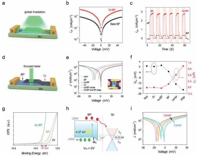
Fig. 2a shows the schematic illustration of the Gr-BP device. For comparison, bare BP device with similar thickness was also tested. As shown in Fig. 2a, the electrode attached with Gr was chosen as drain throughout the whole measurements unless otherwise specified. Fig. 2b shows the plot of photo-induced current density (Iph) versus bias (Vds) of bare BP and Gr-BP devices under global irradiation (532 nm, 1 mW/mm2). It is seen that Gr-BP devices show higher output Iph over a Vds range from -0.05 V to +0.05 V and fast on-off photoresponse (Vds = +0.05 V, Fig. 2c). To assess the performance of our device, photoresponsivity (R) and external quantum efficiency (EQE), the figures of merit of photodetector devices, are calculated according to the following equations [3, 8]:

|
(1) |
|
(2) |

|
Download:
|
| Fig. 2. Photoresponse behavior and Gr-BP heterostructure. (a) Sketches of G-BP heterostructure under global illuminations. For the Gr-BP device, single-layer graphene was used as a source electrode. (b) Iph-Vds characteristics of bare BP and Gr-BP device under global laser irradiation with the same laser intensity. (c) Photoresponse behavior comparison between bare BP and Gr-BP devices. (d) Schematic diagram of Gr-BP heterostructure. (e) J-V curves of Gr-BP device with laser focusing on different regions. Inset shows the optical image of the device marked with different color spots for clarification. (f) VOC and ISC of the Gr-BP device with various parts exposed to laser illumination. (g) UPS data of bare Gr, bare BP and Gr-BP heterostructure. (h) Thermal equilibrium energy band alignment of the separated integral parts with Vds = 0 V. (i) Power-dependent photoelectric behavior of Gr-BP heterostructure. | |
where Iph is the photocurrent induced by incident light, P stands for the light intensity, S is the effective area under illumination, λ is the wavelength of the incident light, h, c and e represent the Plank constant, the velocity of light and the charge of the electron, respectively. Based on Eq. 1, the photoresponsivity of Gr-BP heterojunction is significantly enhanced (~672%) over the bare BP device, increasing from 3.6 × 10² mA/W to 2.8 × 10³ mA/W and the corresponding EQE increases dramatically up to 648% from 84%, which are higher than previously reported metrics of BP-based photodetectors (Table S1 in Supporting information) [3, 8].
In order to investigate if the Gr-BP interface contributes to enhanced photoresponse by charge separation or built-in potential, a scanning photocurrent microscope (SPCM) equipped with a focused laser beam was used to identify individual contribution (sketched in Fig. 2d). Fig. 2e shows the J-V (where J represents current density) curves with the laser-focused at five regions (as marked in the right insert). All five regions show photo-response but with different magnitudes (Fig. S4 in Supporting information). A weak rectifying behavior was observed with photocurrent increasing at Vds > 0 V but decreasing at Vds < 0 V, revealing the existence of a small potential barrier that modulates the polarity of current flow. Among the five regions, the Gr-BP junction shows the highest photocurrent of 3.4 × 10⁵ mA/cm2 (Jdark ~1.96 × 10⁵ mA/cm2, Vds = +0.05 V), thus it is responsible for the dramatic differences in photocurrent between bare BP and Gr-BP devices (as exhibited in Figs. 2b and c). Notably, the output of the Gr-BP device presents photovoltaic characteristic. Fig. 2f shows the short-circuit current (Isc) and open-circuit voltage (Voc) acquired under light illumination with a power of ~1.2 mW. Among them, the Gr-BP heterojunction shows the highest photocurrent, especially at its edge region, might be due to energy band depletion at the edge that generates potential at the edge and contributes to the output current (Figs. S4 and S5 in Supporting information). The existence of Voc (−0.013 V) and Isc (0.6 µA) proves that the photoresponse behavior of the Gr-BP device is dominated by the photovoltaic effect rather than thermal driven processes [4].
To determine the band alignment between Gr and BP, ultraviolet photoelectron spectroscopy secondary electron cut-off energies of bare BP flake, bare graphene films, and Gr-BP heterostructure (Fig. 2g). Accordingly, their work functions are measured to be ФBP = 4.47 eV, ФGr = 4.50 eV and ФGr-BP = 4.37 eV (see Experimental section in Supporting information for calculation details), respectively, which are in good agreement with the previous reports [30-32]. Based on the above values, we can conclude that graphene is n-doped (~0.13 eV), and BP flake becomes highly p-doped with EF ~0.02 eV above the valence band maximum (EVBM). With this information, the energy band diagrams are constructed as shown in Fig. 2h. For Gr-BP device, due to the initial p-doping of BP (possibly originating from impurities and defect, Figs. S6 and S7 in Supporting information for XPS and STM data), downward band bending occurs at the interface to create a built-in potential (Фbi) proportional to ФGr-EVBM (~0.09 ± 0.03 eV). Due to the built-in potential, Gr-BP heterojunction shows a rectifying behavior (Fig. 2i). Upon photo-excitation, e-h pairs are generated in BP; after exciton dissociation, electrons are injected into a more conductive graphene layer, while the Schottky barrier at the interface blocks hole transport to graphene [32-34].
Next, the photoresponse of Gr-BP heterojunction is electrostatically modulated using a back gate. Fig. 3a shows the Ids-Vg data of the Gr-BP device with and without ~1.4 mW laser illumination (Vds = +0.1 mV). In the dark, the Gr-BP device shows ambipolar and hole-dominant characteristics with hole mobility ~1320 cm−2 V −1 s −1 and electron mobility ~745 cm−2 V −1 s −1. These values are two times larger than those of the bare BP device with the similar thickness (see Fig. S9 in Supporting information for bare BP device). Upon photo-irradiation, the photocurrent monotonically decreases with Vg ranging from −50 V to around +27.5 V; this is followed by a sharp decline, and then the photocurrent becomes negative when Vg > ~36.3 V. Fig. 3b shows the gate-tunability of output I-V characteristics from the same device (see the dark and illuminated current comparison in Fig. S10 in Supporting information). Fig. 3c shows that the polarities of photocurrents (Iph, here Vds = +0.05 V) are opposite at negative and positive gate regimes; there is a higher current at negative gate voltage compared to positive gate voltage, which allows the types and heights of Schottky barrier across the Gr-BP junction to be determined. When Vg < 0 (Fig. 3d), the accumulation of holes at BP increases the downward band bending. Therefore, the wider depletion region (W) and larger potential barrier height (Фbi) prevent the tunneling or thermal injection of holes from BP into graphene. In this regime, the photocurrent increases monotonically with the magnitude of the negative gate voltage. In contrast, a positive gate voltage (0 < Vg < Vcritial, Fig. 3e) reduces the barrier height as well as the depletion width in the BP layer, thus allowing holes to overcome the barrier through thermal emission process and recombine with electrons, as a result, the photocurrent gradually decreases at higher positive gate voltage. At even higher positive gate voltage (Vcritial < Vg, Fig. 3f), the EF is shifted closer to the conductance band, and the band bending reverses, thus the channel becomes n-type. The Schottky barrier height (Фn) at the CB and depletion region in the BP flake gradually dominates the charge transfer at the interface by suppressing photo-excited electron from BP, leading to a reversal of the direction of the photocurrent.

|
Download:
|
Fig. 3. Gate-dependent photoelectric behavior of Gr-BP heterostructure. (a) R(Vg) data in Gr-BP device with and without light illuminations. Vds = +0.1 mV. Inserted is the plot of conductance vs gate curve of Gr-BP device in dark. FET mobility is given by  |
|
We performed density functional theory (DFT) calculation to investigate gate-modulated electronic properties of Gr-BP heterostructure to gain more insight. The interlayer distance between graphene and bi-layer BP (Fig. 3g) is calculated to be 3.45 Å. This vdW gap confirms the weak nature of the interfacial interaction, in good agreement with previous studies [35-37]. Fig. 3h shows the electronic band structure of Gr-BP heterostructure, from which it is clear that both the projected band structures of graphene and BP maintain the characteristics of the isolated counterparts upon their contact. The VBM of BP is close to the Fermi level of graphene and a p-type semiconductor/metal Schottky barrier is present. Due to the weak screening effect of BP and Gr, the contact barrier at the BP-Gr interface can be surmounted effectively by applying an external perpendicular electric field (Eext) [35]. By considering Gr as the metal contact and few-layer BP as the semiconductor channel, the Schottky barrier height (SBH) could be estimated following Schottky-Mott rule, Eg = qФp + qФn, where Фp and Фn represent the barriers against the hole and electron flow between Gr and BP, respectively [38]. Fig. 3i depicts the evolution of the contact barriers as a function of the applied electric field strength (see Fig. S11 in Supporting information for the evolution of band structure as a function of Eext). Subjected to a negative electric field (Eext < 0 V), the Dirac cone of graphene shifts towards the VB of the BP, rendering the contact ohmic. In contrast, for increasing positive Vg, the Dirac cone gradually moves towards the CB of BP. When the electric field is larger than 2 eV/nm, the contact barrier Фp becomes smaller than Фn, turning the contact into n-type. These theoretical findings agree well with our experimental observation. We would like to point out that the layer-dependent bandstructure of BP, initial p-doping level and the approximation of exchange-correlation functionals render it highly challenging to calculate the exact barrier height, but the trend of the charge transfer and barrier variation with applied electric field is valid and consistent with the experimental observation.
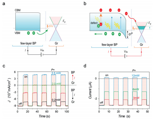
In Gr-BN [34], BP-ZnO [39] and BP-TiOx [40] system, a tunable photo-induced electron transfer has been reported at the interface. Spatial segregation of holes and electrons occurs at different layers, which rearranges the band alignment between two components. Similarly, we found that the Gr-BP heterostructure is capable of showing photo-induced electron transfer. Since absorbents and moisture easily contaminate graphene, all measurements were conducted in a vacuum cell, and thermal annealing was carried out to remove any impurities. Figs. 4a and b illustrate the origins of the photo-doping induced inversion. In the dark state (Fig. 4a), when BP is positively biased, the direction of the current is from BP to graphene. Upon laser illumination (Fig. 4b), electrons are photo-excited from donor-like defects in BP to the conduction band; some of these electrons compensate the holes in BP, while excess electrons created by higher laser photoexcitation migrate to graphene and gives rise to a reverse current. In addition, this migration lifts the EF of graphene while lowering the EF of BP, as a result, band realignment occurs. A direct proof of the photo-induced doping effect is the shifting of Dirac point of graphene in Gr-BP FET device (all graphene placed on top of BP flake, Fig. S13 in Supporting information) upon illumination, where the charge neutral point of graphene shifts to higher negative gate voltage (∆ ~6 × 1011 cm−2), illustrating graphene becoming n-doped and the occurrence of photo-induced charge transfer. Fig. 4c shows the power-dependent J-T curves of Gr-BP heterojunction (edge region) under Vds = −0.01 V. In the dark, a current flow from BP to Gr with the value of 9.0 × 10⁴ mA/cm2 is initially observed when the BP side is positively biased; this current gradually decreases with increasing laser irradiation power and becomes closed at 2.0 mW laser exposure. Most interestingly, the direction of photocurrent reverses at higher laser power (P ≥ 2.0 mW). When the laser moves into the center region of Gr-BP heterostructure, ~3.0 mW laser power or larger is required to invert the current flow direction (see Fig. S14 in Supporting information for J-T curves) [41]. Moreover, this trend could be extended to a larger negative bias. For instance, under Vds = −0.05 V, an excitation laser with a power larger than ~12 mW (Fig. 4d) is required to reverse the polarity of current flow. The ability to control the polarity of the current by adjusting the power of the laser is a unique feature of the Gr/BP junction, which is not shared by monolayer graphene or BP flake (Fig. S13d). For bare BP, although the photocurrent is proportional to the intensity of irradiation due to thermal driven effects, the polarity of current remains the same with the initial current flow for all laser intensity range.

|
Download:
|
| Fig. 4. Photo-inverter behavior of Gr-BP heterostructure. (a) Band alignment of BP and Gr device with a negative source-drain bias in dark. The current flow is from BP to graphene. (b) Band re-alignment of BP and Gr heterostructure due to photo-induced doping effect. Under intense light irradiation, a reverse current flow occurs from graphene to BP. (c) Photogenerated current of Gr-BP device under different laser power density at Vds = −0.01 V. (d) Photogenerated currents of Gr-BP device with Vds = −0.05 V under 3, 6 and 12 mW laser exposure. | |
There are several reasons why the Gr/BP interface is unique in terms of its gate tunability. The small band gap (~0.3 eV) and absence of interfacial pinning effect allow multilayer BP to be switched readily between the hole and electron-dominated transport under a moderate electric field, thus giving rise to ambipolar transport. In accordance with nonlinear Thomas-Fermi theory [12, 13], the electrostatic screening behavior of multilayer BP (thickness ≤ 10 nm) is intermediate, thereby allowing the electric field from the back gate penetrating BP multilayer to influence the properties of graphene in Gr-BP heterostructure. In addition to maintain similar response time (Fig. S15 in Supporting information), the encapsulation of BP flake by the graphene layer not only overcomes the air instability of BP but also increases the photoresponsivity of BP via the formation of a Schottky barrier [42].
We have demonstrated that Gr-BP heterostructures can be used as photodetectors and photoinverters. Comparing with bare BP device, the photoresponsivity increases to 672% (R ~2.8 × 10³ mA/W) due to the presence of a Schottky barrier at the interface of p-type BP and graphene. The height of the Schottky barrier can be modulated by either electrostatic doping or photo-induced doping, allowing the initial p-type conducting channel to be converted to n-type. The highly tunable nature of the Gr-BP interface suggests its potential application in future optoelectronic and logic applications.
Declaration of competing interestThe authors declare that they have no known competing financial interests or personal relationships that could have appeared to influence the work reported in this paper.
AcknowledgmentsThe authors wish to acknowledge the financial support provided by the Fundamental Research Funds for the Central Universities (Nos. NS2020008, NC2018001, NJ2020003, NZ2020001), the Program for Innovative Talents and Entrepreneur in Jiangsu, Research Fund of State Key Laboratory of Mechanics and Control of Mechanical Structures (Nos. MCMS-I-0419G02, MCMS-I-0421K01), National Key Research and Development Program of China (No. 2019YFA0705400), and Australian Research Council Future Fellowship (No. FT160100205), DECRA Fellowship (No. DE200101622).
Supplementary materialsSupplementary material associated with this article can be found, in the online version, at doi:10.1016/j.cclet.2021.06.079.
| [1] |
Y.Yu Li, G.J. Ye, et al., Nat. Nanotechnol. 9 (2014) 372-377. DOI:10.1038/nnano.2014.35 |
| [2] |
F.N. Xia, H. Wang, Y.C. Jia, Nat. Commun. 5 (2014) 4458. DOI:10.1038/ncomms5458 |
| [3] |
M. Buscema, D.J. Groenendijk, S.I. Blanter, et al., Nano Lett. 14 (2014) 3347-3352. DOI:10.1021/nl5008085 |
| [4] |
T. Low, M. Engel, M. Steiner, P. Avouris, Phys. Rev. B 90 (2014) 081408. DOI:10.1103/PhysRevB.90.081408 |
| [5] |
H. Yuan, X. Liu, F. Afshinmanesh, et al., Nat. Nanotechnol. 10 (2015) 707-713. DOI:10.1038/nnano.2015.112 |
| [6] |
N. Youngblood, C. Chen, S.J. Koester, M. Li, Nat. Photon. 9 (2015) 247-252. DOI:10.1038/nphoton.2015.23 |
| [7] |
Q. Guo, A. Pospischil, M. Bhuiyan, et al., Nano Lett. 16 (2016) 4648-4655. DOI:10.1021/acs.nanolett.6b01977 |
| [8] |
D. Xiang, C. Han, J. Wu, et al., Nat. Commun. 6 (2015) 6485. DOI:10.1038/ncomms7485 |
| [9] |
Y.J. Xu, J. Yuan, L. Fei, et al., Small 12 (2016) 5000-5007. DOI:10.1002/smll.201600692 |
| [10] |
M. Freitag, T. Low, F. Xia, P. Avouris, Nat. Photon. 7 (2013) 53-59. DOI:10.1038/nphoton.2012.314 |
| [11] |
W.J. Yu, Y. Liu, H. Zhou, et al., Nat. Nanotechnol. 8 (2013) 952-958. DOI:10.1038/nnano.2013.219 |
| [12] |
T. Low, R. Roldán, H. Wang, et al., Phys. Rev. Lett. 113 (2014) 106802. DOI:10.1103/PhysRevLett.113.106802 |
| [13] |
Y. Liu, Z. Qiu, A. Carvalho, et al., Nano Lett. 17 (2017) 1970-1977. DOI:10.1021/acs.nanolett.6b05381 |
| [14] |
J.P. Lu, A. Carvalho, J. Wu, et al., Adv. Mater. 28 (2016) 4090-4096. DOI:10.1002/adma.201506201 |
| [15] |
A.K. Geim, I.V. Grigorieva, Nature 499 (2013) 419-425. DOI:10.1038/nature12385 |
| [16] |
H. Fang, C. Battaglia, C. Carraro, et al., PNAS 111 (2014) 6198-6202. DOI:10.1073/pnas.1405435111 |
| [17] |
Q.H. Wang, K. Kalantar-Zadeh, A. Kis, et al., Nature Nanotechnol. 7 (2012) 699-712. DOI:10.1038/nnano.2012.193 |
| [18] |
S.Z. Butler, S.M. Hollen, L. Cao, et al., ACS Nano 7 (2013) 2898-2926. DOI:10.1021/nn400280c |
| [19] |
F.H.L. Koppens, T. Mueller, P. Avouris, et al., Nat. Nanotechnol. 9 (2014) 780-793. DOI:10.1038/nnano.2014.215 |
| [20] |
C.H. Lee, G.H. Lee, A.M. van der Zande, et al., Nat. Nanotechnol. 9 (2014) 676-681. DOI:10.1038/nnano.2014.150 |
| [21] |
K. Roy, M. Padmanabhan, S. Goswami, et al., Nat. Nanotechnol. 8 (2013) 826-830. DOI:10.1038/nnano.2013.206 |
| [22] |
B.W. Baugher, H.O. Churchill, Y. Yafang, P. Jarillo-Herrero, Nat. Nanotechnol. 9 (2014) 262-267. DOI:10.1038/nnano.2014.25 |
| [23] |
O. Lopez-Sanchez, D. Lembke, M. Kayci, A. Radenovic, A. Kis, Nat. Nanotechnol. 8 (2013) 497-501. DOI:10.1038/nnano.2013.100 |
| [24] |
M. Buscema, D.J. Groenendijk, G.A. Steele, et al., Nat. Commun. 5 (2014) 4651. DOI:10.1038/ncomms5651 |
| [25] |
W.J. Yu, Z. Li, H. Zhou, et al., Nat. Mater. 12 (2013) 246-252. DOI:10.1038/nmat3518 |
| [26] |
E.Gaufres A.Favron, F. Fossard, et al., Nat. Mater. 14 (2015) 826-832. DOI:10.1038/nmat4299 |
| [27] |
A. Das, S. Pisana, B. Chakraborty, et al., Nat. Nanotechnol. 3 (2008) 210-215. DOI:10.1038/nnano.2008.67 |
| [28] |
D. Hanlon, C. Backes, E. Doherty, et al., Nat. Commun. 6 (2015) 8563. DOI:10.1038/ncomms9563 |
| [29] |
J. Lu, J. Wu, A. Carvalho, et al., ACS Nano 9 (2015) 10411-10421. DOI:10.1021/acsnano.5b04623 |
| [30] |
Y. Liu, L. Yuan, M. Yang, et al., Nat. Commun. 5 (2014) 5461. DOI:10.1038/ncomms6461 |
| [31] |
Y.J. Yu, Y. Zhao, S. Ryu, et al., Nano Lett. 9 (2009) 3430-3434. DOI:10.1021/nl901572a |
| [32] |
J.E. Padilha, A. Fazzio, A.J. da Silva, Phys. Rev. Lett. 114 (2015) 066803. DOI:10.1103/PhysRevLett.114.066803 |
| [33] |
L. Li, G.J. Ye, V. Tran, et al., Nat. Nanotechnol. 10 (2015) 608-613. DOI:10.1038/nnano.2015.91 |
| [34] |
L. Ju, , E. Huang, et al., Nat. Nanotechnol. 9 (2014) 348-352. DOI:10.1038/nnano.2014.60 |
| [35] |
J.E. Padiha, A. Fazzio, A.J.R. da Silva, Phys. Rev. Lett. 114 (2015) 066803. DOI:10.1103/PhysRevLett.114.066803 |
| [36] |
H. Guo, N. Lu, J. Dai, et al., J. Phys. Chem. C 118 (2014) 14051-14059. DOI:10.1021/jp505257g |
| [37] |
Y.Q. Cai, G. Zhang, Y.W. Zhang, J. Phys. Chem. C 119 (2015) 13929-13936. DOI:10.1021/acs.jpcc.5b02634 |
| [38] |
P.A. Khomyakov, G. Giovannetti, P.C. Rusu, et al., Phys. Rev. B 79 (2009) 195425. DOI:10.1103/PhysRevB.79.195425 |
| [39] |
Z. Xia, P. Li, Y. Liu, et al., Nano Res. 10 (2017) 3848-3856. DOI:10.1007/s12274-017-1598-z |
| [40] |
P.H. Ho, M.K. Li, R. Sankar, et al., ACS Photon. 3 (2016) 1102-1108. DOI:10.1021/acsphotonics.6b00192 |
| [41] |
M. Huang, M. Wang, C. Chen, et al., Adv. Mater. 28 (2016) 3481-3485. DOI:10.1002/adma.201506352 |
| [42] |
Y. Huang, J. Qiao, K. He, et al., Chem. Mater. 28 (2016) 8330-8339. DOI:10.1021/acs.chemmater.6b03592 |