 2022, Vol. 33


b State Key Laboratory of Chemical Biosensing and Chemometrics, College of Chemistry and Chemical Engineering, Institute of Chemical Biology and Nanomedicine (ICBN), Hunan University, Changsha 410082, China
Current semiconductor technology now is facing serious limitation in performance enhancement due to the short channel effect and excessive power generation. Two-dimensional (2D) semiconductors with ultra-thin body exhibit strong immunity to short channel effect [1], making them the promising material platform for building next generation nanoelectronics [2]. Since the discovery of the gap-less semi-metallic monolayer graphene, a large variety of 2D semiconductors with a finite electronic band gap, including black phosphorus, transition metal dichalcogenides and transition metal monochalcogenides, have been discovered. They possess unique properties such as high carrier mobility [3], tunable bandgap [4], anisotropic transport [5-7], leading to the various applications in the fields of electronics and optoelectronics, such as transistors [8, 9], sensors [10, 11], light-emitting devices [12], memory devices [13, 14], nanoelectromechanical device [15, 16], electrochemical devices [17, 18]. However, research towards the realization of the 2D semiconductors based future electronic and photonic devices faces serious challenges, as most of the currently discovered 2D semiconductors are known to be air reactive [19]. Their properties may degrade significantly with time when exposing them to ambient conditions due to the considerable oxidation. Hence, the air stability of 2D materials is key to the investigations of their fundamental properties and for their potential applications in devices. Understanding the fundamentals behind the oxidation, especially the key factors in air oxidation, allows us to intentionally prevent 2D semiconductors from contain conditions, therefore prolonging their lift time in ambient. Moreover, the appropriate methodologies can be developed for 2D materials accordingly to stop the ambient oxidation completely without changing their intrinsic properties.
Here, we review the recent progress on the fundamentals and applications of the oxidations of 2D semiconductors. In particular, we focus on these comprehensively investigated 2D semiconductors with certain reactivity, i.e., black phosphorus, transition metal dichalcogenides and transition metal monochalcogenides, in which the air oxidation is a big concern but technically could be carefully avoided. The extremely reactive 2D semiconductors, such as silicene and germanene, are not covered in this review. This review will start with the mechanisms of the air oxidation with the consideration of the impacts from moisture, heat and light. Then two passivation techniques will be introduced, namely the physical capping and chemical surface modification. In the end, the controlled oxidations induced by various techniques and their emerging applications, such as materials patterning, modification and dielectric synthesis, will be presented.
2. Air oxidations and mechanisms 2.1. Black phosphorusBlack phosphorus is a promising layered direct bandgap semiconductor with high room temperature carrier mobility of 1000 cm2 V−1 s−1. When reducing its thickness, its bandgap can be significantly increased from around 0.3 eV in the bulk form to 2 eV in the atomic monolayer [20]. BP is the most thermodynamically stable allotrope of phosphorus. However, in contrast to the chemically inert graphene, BP exhibits the relatively poor air stability, therefore hindering the practical applications of BP-based electronic devices. The oxidation process in BP and its mechanism have been intensively studied.
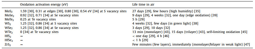
On the surface, the oxidation starts from physisorption of O2 molecules. Then they dissociate into two oxygen atoms to chemisorb on the surface by overcoming a certain activation energy. In the case of BP, the low activation energy of 0.54 eV was calculated based on density functional theory, making it an active material in air [21]. In experiments, using optical microscopy or atomic force microscopy (AFM), small topographic protrusions can be observed on the fresh BP surface shortly after the exfoliation in the air (Fig. 1a). Both the density and the height of these protrusions increase with elongated exposure to the air. Eventually, these small protrusion coalesces and covers the surface after serval days, indicating the full degradation of BP. Measurements of X-ray photoelectron spectroscopy (XPS) and electron energy loss spectroscopy (EELS) in scanning transmission electron microscopy reveal that the rapid material degradation of BP is due to the formation of phosphorus oxide [22, 23]. The formation of phosphorus oxide POx is noted upon the exposure to air (Fig. 1b). Moreover, as oxidation inevitably breaks the crystalline structure of pristine BP, it is also able to monitor the oxidation progress with Raman spectroscopy.

|
Download:
|
| Fig. 1. (a) AFM height images of BP flake measured at varied air exposure duration after exfoliation. Reprinted with permission [22]. Copyright 2014, American Chemical Society. (b) EELS spectra measured on the pristine BP and after one-day air exposure. Reprinted with permission [23]. Copyright 2016, American Chemical Society. (c) AFM images of air-exposed BP flakes showing degradation with respect to time, upon exposure to different optical wavelengths. Reprinted from [24] under CC BY 4.0. | |
In air ambient, the oxidation of BP is found to be a combined effect with the contributions from oxygen, humidity and light. Light is known as the excitation source to produce reactive oxygen species, i.e., O2− to initiate oxidation chemical reaction, without which the oxidation reaction is hard to proceed. Favron et al. reported that, by isolating the light illumination, the complete oxidation of a 5-nm-thick BP can be slowed down by 5 times compared to that in the light ambient [24]. Ahmed et al. determined the influence of discrete wavelengths ranging from ultraviolet to infrared on the oxidation of BP [25]. No obvious change of surface morphology was measured by AFM on BP illuminated with wavelengths longer than 565 nm (Fig. 1c). Hence, they concluded that ultraviolet bandwidth of the spectrum is the primary factor in the photo-oxidation of BP in ambient conditions.
The oxidation of BP becomes more severe in the thinner flakes. The visible surface degradation appears within several hours in few-layer BP. For instance, a Raman spectroscopy measurement showed that a 5-nm-thick BP fully degrade in 20 min with the continuous air exposure [25]. One consideration is the thickness-dependent bandgap of BP, which gradually decreases as the thickness increases. This makes the conduction band minimum closer to O2 acceptor state and eventually drops below it, therefore leading to the reduced rate of charge transfer and hence slower oxidation.
In addition, Walia et al. reported that the coexistence of humidity and light at BP surface can significantly accelerate the oxidation of BP [26]. In contrast to the rapid oxidation of BP kept in light and humid air, fresh exfoliated BP in a desiccator in the absence of both light and humidity can maintain its crystalline for more than eight days with only slight decreases in the intensities of the Raman modes. The roles of oxygen and water have been investigated separately by removing the influence of others. In the following, we will discuss the oxidation of BP under controlled conditions. Naclerio et al. performed an in situ transmission electron microscopy measurement under 80 kV electron-beam on few-layered BP exposed to ultra-low pressure oxygen condition [27]. Before the introduction of oxygen, BP was found to be rather stable without showing visible degradation under the irradiation of 80 kV electron beam. When a low oxygen of 2.5 × 10⁻⁶ Torr oxygen was added, an amorphous phosphorus oxide POx layer are observed with its thickness that correlated to the oxygen partial pressure. Here, the electron beam could provide the additional activation energy or atomic oxygen radicals by dissociating O2 molecules to accelerate the oxidation process. Oh et al. studied the surface oxidation of BP exposed to pure oxygen by in situ ultra-high-vacuum photoelectron spectroscopy. The high resolution P 2p core-level spectra shows that the oxidation starts from the bonding of P atoms to one and two O atoms. Then other components of incomplete P2O5 with higher binding-energy rapidly grow and chemically bonded to BP [28].
Ab initio calculations reveals that pure water cannot chemically react with pristine BP even its appearance can accelerate the oxidation process of BP in the air. In fact, the pristine BP surface is hydrophobic and H2O molecules can only physisorb on the surface of BP via hydrogen bonds. Huang et al. utilized isotopically different oxygen atoms 18O and 16O as label to distinguish the oxidation caused by oxygen and water. They found that the exposure to deaerated or N2 bubbling O2 depleted water cannot lead to obvious oxidation on BP even in the case of the monolayer and bilayer BP [23]. However, the BP surface is polarized once oxygen atoms are chemisorbed. Subsequently, it becomes more hydrophilic. The oxidation of BP with the appearance of water is therefore strongly affected by the existing surface oxidation. H2O can form one hydrogen bond with the lone-pair oxygen on the oxidized surface. Hence, phosphoric acid species (HxPOy) are formed on the surface and lead to further oxidation in the underlying layers.
2.2. Transition metal dichalcogenides2D transition metal dichalcogenide materials in the form of MX2, where M represents a transition metal atom (e.g., Mo, W, Zr and Hf) and X represents a chalcogen atom (e.g., S, Se, Te), have received tremendous attentions due to their intrinsic band structures. The air stability of TMDs is an important issue for their device applications. Unlike BP, most of the TMDs are stable under ambient conditions.
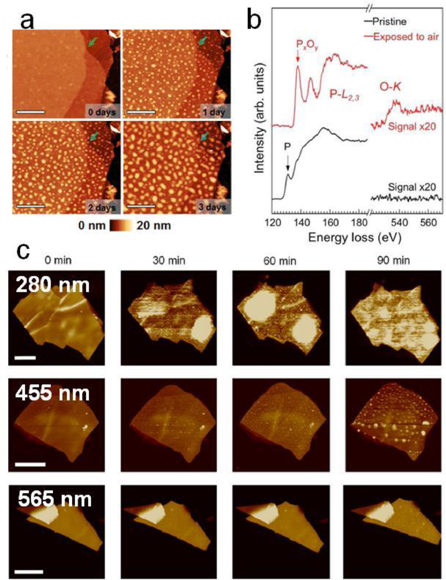
MoS2 is the most intensively studied group-VIB TMD. It is normally also considered as the most stable material upon air exposure. Exfoliated single crystalline MoS2 surface did not show any noticeable features or surface change under AFM in the long air exposure up to 27 days, implying that it is the most suitable TMD for electronic applications from a material point of view [29]. Theoretical calculations showed a high activation energy of 1.59 eV is required to dissociate O2 molecule on the pristine MoS2 monolayer (Fig. 2a) [30]. Nevertheless, SEM analysis showed that on the exfoliated MoS2 the oxidation could occurs at the flake edges, resulting in partially oxidized edges [31]. This can be ascribed to a much reduced oxygen dissociation barrier as low as 0.31 eV at the edge sites [30, 32]. In addition to the chemically active edges, sulfur vacancies residing on the surface of MoS2 also offer the possible sites for initiating oxidation with the much lowered kinetic barrier < 0.80 eV (Fig. 2a) [30, 33, 34]. Clear oxidation induced defective features were observed on the surface of MoS2 using STM and Raman spectroscopy, which can be promoted by rising the temperature. It was found that when exposing MoS2 to water, partial etching of the surface layer and the formation of needle-like protrusions were observed on its surface (Fig. 2b) [35]. XPS and atomic absorption spectroscopy (AAS) analyses showed that this behavior might arise from the oxidation of MoS2 into MoO3 and SO42–.

|
Download:
|
| Fig. 2. (a) Oxygen dissociative adsorption barrier on pristine MoS2 surface and defective surface with a Sulphur vacancy. Reprinted with permission [30]. Copyright 2015, AIP publishing. (b) AFM images of a fresh MoS2 surface and after immersion in water for 12 h. Reprinted with permission [35]. Copyright 2017, American Chemical Society. | |
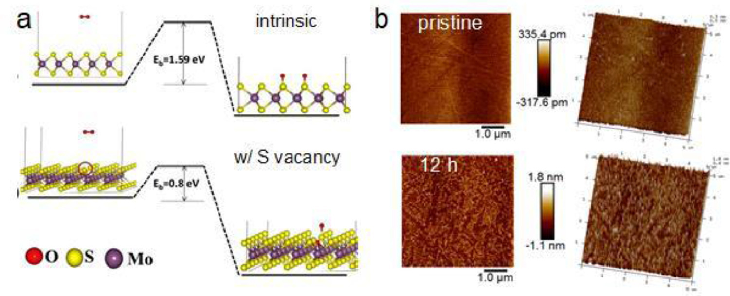
Although WS2 is more reactive to oxygen than MoS2, the interior oxidation of single crystalline WS2 upon the exposure to oxygen is still difficult to happen due to the high kinetic barrier of 1.25 eV [32, 36]. XPS measurement only detected a very low oxygen concentration of ~2% and an unchanged O 1s level after 4 weeks of air exposure. Similar to MoS2, the air oxidation of WS2 in the air ambient can be initiated by water exposure or rising the reaction temperature. Liu et al. preformed thermal oxidation at 400 ℃ [37]. The oxidation started from the edges which have the lower activation energy, then it propagated laterally toward the center (Fig. 3a). Moreover, Kotsakidis et al. reported the clear photo-induced oxidation in the exposed WS2 in the presence of 532 nm green light [38].

|
Download:
|
| Fig. 3. (a) Optical microscopy picture showing the oxidized edges of air-exposed WSe2 and Raman intensity plots taken at the center and edge of the flake. Reprinted with permission [37]. Copyright 2015, American Chemical Society. (b) Raman spectra of monolayer and trilayer WTe2 samples over time in ambient condition. Reprinted with permission [43]. Copyright 2016, Wiley-VCH Verlag GmbH & Co. KGaA, Weinheim. (c) Energy-dispersive X-ray mapping showing the formation of Se blister on the surface of the oxidized HfSe2 flake. The regions below the blister are depleted of Se. Reprinted with permission [29]. Copyright 2016, AIP Publishing. | |
It is known that the TMDs become less resistance to oxidation when changing the chalcogen from S to Se and then to Te. For instance, the kinetic barrier for oxygen dissociation reduces from 1.59 eV to 0.92 eV, when changing from MoS2 to MoSe2 [32]. Nevertheless, same as sulfides, the oxidation begins from the edges of selenides while the single crystalline surface is nearly inert to air within a 1-day exposure [39]. Theoretically, the surface of the single crystalline tellurides, such as MoTe2 and WTe2, should also be considerably air inert, even they are most reactive among the group-VIB TMDs. In reality, tellurides have a low structural stability and are prone to create Te vacancies at slightly increased temperature or with light illuminations [40-42], at which the activation energy is much reduced [34]. WTe2 is unique among group-VIB TMDs as it crystallizes in a distorted 1T′ phase. Monolayer WTe2 is known to be extremely reactive in air [43], which even possesses a zero activation energy at the tellurium vacancy sites [34]. Its characteristic Raman peaks vanished within 13 min after exfoliation due to the oxidation in air (Fig. 3b). In comparison, the Raman signals were still identified after 15 days in the bilayer and trilayer WTe2. Interestingly, the oxidation of tellurium-containing TMDs in air is complex due to the reactive of tellurium which results in α-TeO2. XPS measurements showed clear signal of TeO2 and MoOx/WOx in the air exposed MoTe2/WTe2 using XPS measurement [43, 44]. In multiple layered MoTe2 and WTe2, the surface oxidation was found to be a self-limiting process, as the resulted MoOx or WOx can act as passivation layers. For instance, using ellipsometry, Hou et al. showed that the surface oxidation is limited when a ~2.5 nm thick amorphous oxide layer was formed on surface of WTe2 single crystal [45].
Group IVB TMDs, such as ZrS2, ZrSe2, HfS2, HfSe2, are indirect band gap semiconductors with large work functions and high mobility which are of great interest for electronic applications. Their air stability of is a matter of concern. Small bubbles due to surface oxidation were found on HfS2 surface after 4 h of oxidation [46]. In the case of HfSe2, the oxidation process proceeds as Se atoms are completely replaced by oxygen atoms to form HfOx while the Se atoms aggregate at the surface with time in the form of blisters as shown in Fig. 3c [29]. In addition, oxidation was severely accelerated at defect sites and by light illumination. No Raman signal can be detected on monolayer and bilayer ZrS2 in air, due to the easy oxidation assisted by the weak laser illumination [47]. Interestingly, flake thickness increased simultaneously during oxidation process. After a long exposure of 120 h, the thickness can be expanded by about 250%. Such expansion can be ascribed to the intercalations of oxygen atoms between layers. exposure to the laser for some minutes The AFM measurements indicates ZrS2 as an air-sensitive TMD, clearly shows a hole of about 1.9 nm produced by the laser over the flake surface. HfSe2 and ZrSe2 are more reactive in air [48, 49]. The oxidation of exfoliated HfSe2 and ZrSe2 in air were studied with cross-section TEM and energy-dispersive X-ray (EDX) mapping [50]. The results indicated amorphous substoichiometric oxides of HfOx and ZrOx grow primarily from the top surface to bottom after few days of ambient exposure. In the case of ZrSe2, the oxidation also occurs at the substrate bottom interface with the laterally diffused oxygen or moisture.
Table 1 lists the calculated oxidation activation energies and observed air life time from experiments of the typical TMDs discussed above as a summarization of their air stabilities.
|
|
Table 1 Summary of the air stabilities of the representative TMDs. |
Group-Ⅳ monochalcogenides – GeS, GeSe, SnS and SnSe, possess the similar orthorhombic lattice with BP. Compared to BP, there are only a few investigations on their air stability. DFT calculations revealed the high activation energies ranging from 1.26 eV to 1.60 eV required for the reaction with oxygen [51], highlighting a good stability of group-Ⅳ monochalcogenides in oxygen. However, experiments have observed clear sign of surface oxidation on Group-Ⅳ monochalcogenides [52]. Clear optical contrast and morphology changes were found on the surface of exfoliated GeS flakes after one-day storage in air (Fig. 4a) [53]. PL and XPS measurements indicated the formation of substoichiometric GeOx. Easily formed Se-vacancies are the possible reasons for the rapid oxidation in air ambient [54]. Regarding water-assisted oxidation, a slightly higher activation energy of O2 dissociation was obtained for GeS monolayer in humid air than that without the presence of H2O using DFT calculations, indicating the low possibility of water-assisted oxidation. However, molecular dynamics simulations indicate a high reactivity of Group-Ⅳ monochalcogenides [55], on which the polar H2O molecules can be dissociated within tens of nanosecond in ambient.

|
Download:
|
| Fig. 4. (a) Optimal microscopy images of an exfoliated GeS flake upon 10-day exposure to air. AFM images showing the evolution within the first 48 h after exfoliation. Reprinted with permission [53]. Copyright 2019, American Chemical Society. (b) Raman spectra of GaSe sample over time in ambient condition. Reprinted with permission [60]. Copyright 2017, AIP Publishing. | |
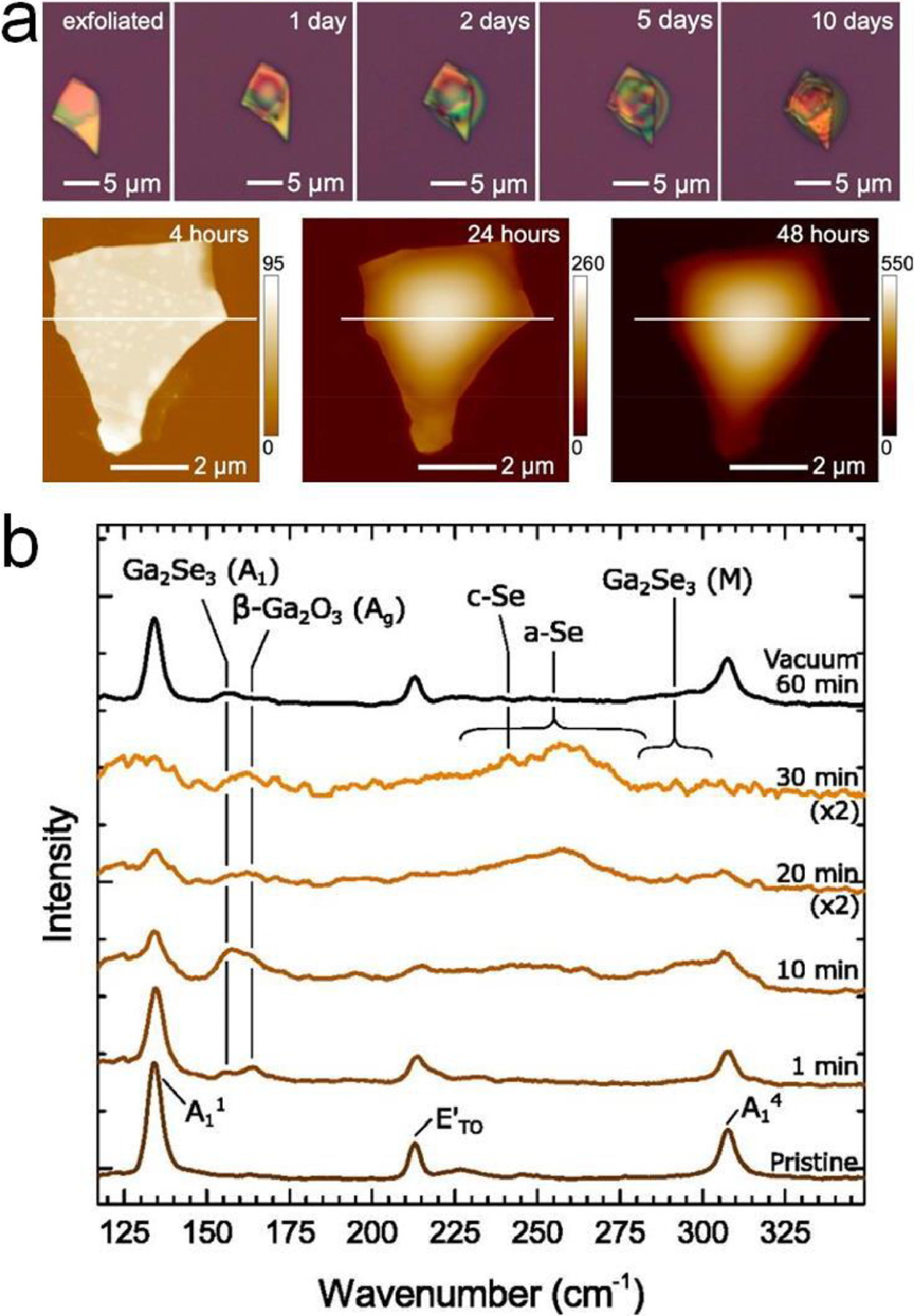
Besides, another group of well-studied transition metal monochalcogenides is the Group-Ⅲ monochalcogenides (GaS, GaSe, InS and InSe), which possess a layered hexagonal structure. Native oxides are commonly noted on their surface after long air storage [56, 57]. The rapid oxidation in mechanically exfoliated GaSe has been observed using Raman spectroscopy (Fig. 4b) [58-60]. In particular, the monolayer reaches an oxidized state almost immediately after exposure to air [61]. The oxidation produces are complex, including Ga2Se3, Ga2O3, and amorphous and crystalline selenium (Fig. 4b). GaSe is also extremely sensitive to light, no safe measurement power therefore exists to carry out accurate optical measurements on ultrathin GaSe in ambient conditions. Similar to group-Ⅳ monochalcogenides, the DFT calculated activation energy required for dissociating O2 molecules are high in the case of Group-Ⅲ monochalcogenides, which are around 3 eV [62, 63]. Theoretically, the spontaneous oxidation in ambient is very unlikely in the perfect group-Ⅲ monochalcogenides. Nevertheless, the chalcogen vacancies are easily formed on the surface due to the low binding energies, at which activation energies are significantly reduced to 0.26~0.36 eV [61]. Hence, the defects are vulnerable to oxidation and provide the highly reactive sites for reaction with water and oxygen in air directly and activate the neighboring chemical bonds for further oxidation [64].
3. PassivationThe air instability of 2D semiconductors seriously limits their practical applications. The key factor in studying the intrinsic properties and unleashing the true potential of two-dimensional materials is to avoid the spontaneous oxidation to the maximum extent. One strategy is to perform all characterization, fabrication and measurements in an oxygen and moisture-free environment. Chae et al. reported the fabrication and measurements of HfS2 field effect transistors in an integrated vacuum cluster system, combined with four glove boxes [46]. Hence, HfS2 can be mostly isolated from oxygen and moisture (< 1 ppm) and therefor exhibits the presumably intrinsic properties. Nevertheless, such a system cannot contain all functionalities required for characterization and device fabrications. When transferring the materials between different instruments, exposure to ambient is inevitable. Therefore, it is of great importance to develop efficient techniques to slow down or ideally to completely eradicate the oxidation under ambient conditions. In this section, various passivation strategies developed till-date will be discussed.
3.1. Physical capping and encapsulationThe most commonly investigated passivation is done by physically protecting the surface of 2D semiconductors from ambient gases using a capping layer. Polymethyl methacrylate (PMMA) polymer, a common electron beam photoresist, can be easily spun on the exfoliated sample to passivate the surface. Although PMMA inevitably dopes the underlying 2D semiconductors, due to the convenience, this has been widely used in the early stage [65, 66]. Air-stable thin film oxides, such as Al2O2, HfO2, which have been utilized to passivate silicon, have been coated on the 2D semiconductors using atomic layer deposition to passivate their surface from oxidation [67, 68]. A 1 nm-thick ALD deposited Al2O3 could effectively slow down the obvious oxidation in the exfoliated few-layer BP from tens of minutes to a month [69]. Using thin-film passivation, the thermal stability of 2D semiconductors can also be much enhanced. With Al2O3 passivation layer, SnS2 can survive in a high temperature annealing of 700 ℃, in comparison, it decomposes and evaporates at 400 ℃ without passivation [70]. In additional, the high-k nature of the oxides could benefit the passivated 2D material with an enhanced carrier motility through the dielectric screening and the stronger gate capacitance for more effective gate tunability in the electronic devices [71, 72]. However, a serious issue requires special attention when using ALD deposited thin film passivation layer. Due to the lacking of dangling bonds, ALD on the hydrophobic nature of the most 2D semiconductors leads to isolated islands instead of continuous film. Oxidation is still expected through the numerous pinholes in the ALD oxides. To overcome this issue, a chemically functionalized surface or a precursor layer to initiate the nucleation is necessary to grow uniform passivation oxide films [73-76]. The unideal interface together with the innegligible defect bands induced by passivation oxides inevitably degrade the intrinsic properties of 2D semiconductors.
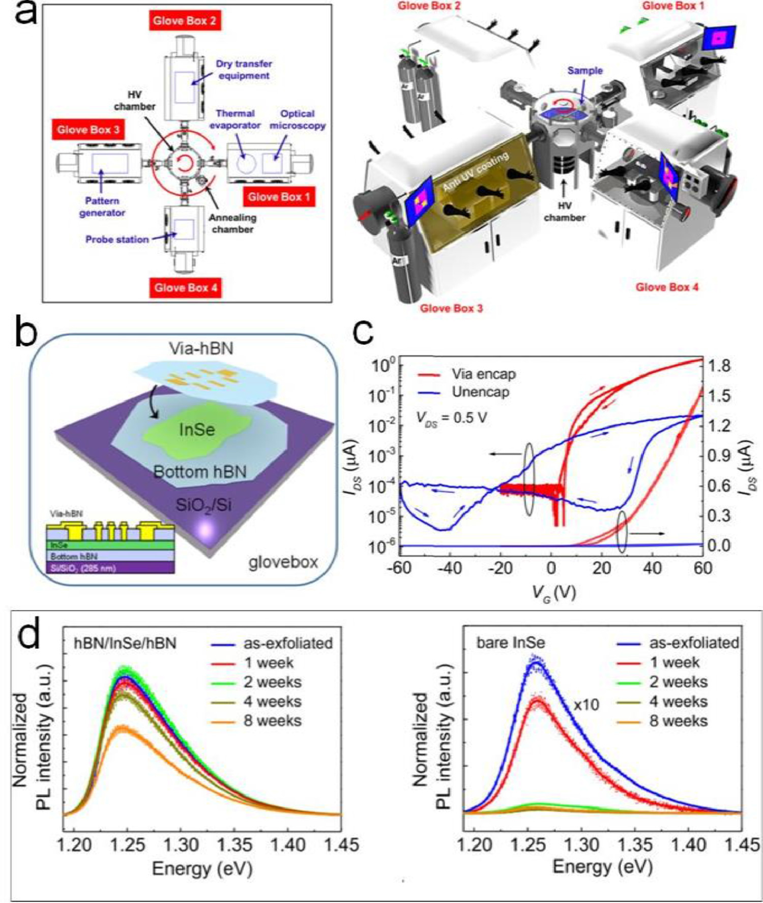
A widely utilized alternative passivation layer other than ALD oxide is the inert 2D hexagonal boron nitride (hBN). By encapsulating the reactive 2D semiconductors prepared in the inert environment with hBN via van der Waals force, the surface of 2D semiconductors is physically protected, which therefore is less susceptible to ambient or even to other reactive chemicals [77]. Thanks to the atomically smooth interface and high quality crystalline of hBN, their intrinsic properties are maintained to the maximum extent [78-80]. For instance, the high hole mobility of 5200 cm2 V−1 s−1 limited by only photon-scattering has been measured in hBN encapsulated BP [81]. The hBN encapsulated InSe exhibits high ambient-stability over an 8-weeks long exposure and shows the nearly negligible hysteresis and an improved mobility of 120 cm2 V−1 s−1 compared to the notable hysteresis and low mobility of ~1 cm2 V−1 s−1 measured in the sample exposed in air (Fig. 5) [82]. The air stability of the half-encapsulated 2D semiconductors requires further validation, as some reports pointed out a slow diffusion of oxygen in between hBN layer and the substrate which causes the oxidation the 2D semiconductors eventually [83].

|
Download:
|
| Fig. 5. (a) Schematic of the integrated vacuum cluster system combined with several gloveboxes in which the air reactive 2D materials can be fabricated and characterized without exposing to ambient. Reprinted with permission [46]. Copyright 2016, American Chemical Society. (b) Schematic of the hBN encapsulate InSe device prepared in a glovebox. (c) Transfer curves of encapsulated and exposed InSe transistor devices. The small arrows show the direction of the gate sweep. (c) Evolution of the PL spectra with time for both encapsulated and exposed InSe at room temperature, respectively, stored under ambient conditions. Reprinted with permission [82]. Copyright 2019, American Chemical Society. | |
Under some circumstances, a dense protection layer grows on 2D semiconductors during synthesis or post-treatment producing self-passivation capability. For instance, GeS synthesized by vapor transport process are self-encapsulated in a thin, sulfur-rich amorphous GeSx shell, which provides GeS exceptional air stability with no changes after 14 days in air [53]. In a more popular case, an oxide layer formed on the surface of few-layer 2D semiconductors, which effectively stop the further oxidation, provides the self-passivation. The controlled oxidation techniques for TMDs include ultraviolet (UV) ozone treatment and oxygen plasma. The oxidation of the topmost layer in MoTe2 subjected to the low power oxygen plasma treatment was found to be efficient to passivate MoTe2 in ambient or even in continuous plasma treatment [84]. Such self-passivation has been reported in oxygen annealed SnS with the surface being oxidized based on the self-limiting process [85] and in the dry-oxidized InSe [57]. One noteworthy problem is that the surface oxides normally bring in significant doping effect to the underlying semiconductor, as will be discussed in details in section Ⅳ.
3.2. Surface modification by organic materialsSurface chemical modification by organic molecules or polymers is another route to passivate 2D semiconductors. Experiments showed that BP can be stabilized by introducing surface functionalization with p-nitrobenzene diazonium [86], and imidazoliu-based ionic liquids [87]. Specifically, aryl diazonium leads to the formation of phosphorus–carbon covalent bonds, which occupy the surface phosphorous atoms, thereby preventing contact between the air mixture and BP surface. Ionic liquids can passivate BP as it effectively depletes the reactive oxygen species on the BP surface. The water-proof linear alkylamines n-CmH2m+1NH2 (m = 4 ~ 11) have been demonstrated as a highly effective passivation for BP and TMDs, including WS2, MoTe2, WTe2, WSe2. Among them, n-hexylamine (m = 6) can be applied in thin molecular monolayer on BP surface with and can prolong the lifetime of BP in ambient from a few hours to months. This passivation monolayer is also stable at high temperature H2 annealing, and general organic solvents, which can be removed by certain organic acids [88]. Except the chemically bonded surface modification, Park et al. demonstrated a monolayer of titanyl phthalocyanine (TiOPc) which forms an organic-inorganic van der Waals interaction on the surface of MoS2 and therefore effectively passivate the defects from oxidations [89]. Xu et al. reported a highly ordered, ultrathin and scalable N, N′-ditridecylperylene-3, 4, 9, 10-tetracarboxylic diimide (PTCDI-C13) as passivation layer for MoS2 which can be grown epitaxially [90].
Generally speaking, organic molecules and polymers can be directly introduced on 2D semiconductors by using solution processing, such as immersion, spin-coating, therefore give the advantageousness of simplicity and low-cost. Albeit these merits, one difficulty of the surface modification is that uniform chemical functionalization may not easy to achieve to fully cover the surface of 2D semiconductors, therefore many exposed regions at the atomic scale may still be reactive in air. In contrast to materials used for physical encapsulations, most of the functionalized organic materials are not stable as the physical encapsulations [91]. Making them surviving from high temperatures or organic solvents during the device fabrication could be an issue. Moreover, the functionalized organics facilitate surface charge transfer doping to the passivated 2D semiconductors, therefore bringing in the unexpected changes of their electric properties. The appropriate molecules with strong binding with the surface or polymers should be carefully chosen.
4. Controlled oxidations and their applicationsAs aforementioned, ideally the basal planes of the majority 2D semiconducting transition metal dichalcogenides and monochalcogenides are air stable considering the high activation energies of the high quality crystalline. The air oxidations only occur without controls from the randomly distributed defects, edges or with the assistant of moisture, heat and light. In additional, for these stable 2D semiconductors, such as MoS2, the oxidation may take hours or even a few days to fully spread over the surface. In order to utilize the oxides, the basal oxidation process must be achieved with controls and relatively rapid rate. There are experimental reports showing oxidations using UV ozone, oxygen plasma, thermal annealing, and scanning probe, with which these factors for accelerating basal oxidation such as UV light illumination, defects, heat can be induced with good controls. In this section, we will present the reported applications on material patterning, modification and synthesis achieved by employing various controlled oxidation processes.
4.1. Material patterningThe energy band structure of some 2D semiconductors highly depend on their thickness. For example, tungsten and molybdenum dichalcogenides exhibit thickness-dependent band gaps where the gaps are enhanced with decreasing thickness [92, 93]. Upon reaching monolayer thickness, they transit from indirect-band gap semiconductors into direct-band gap semiconductors. To tuning their band structures and correlated properties, methodologies that can precisely control the number of layers of 2D semiconductors are highly desired. Surface oxidation based on the self-limiting layer-by-layer process has been demonstrated as an effective way to thin down molybdenum and tungsten chalcogenides with good controls. Self-limited oxidation was reported for WSe2, MoS2 and MoTe2 using oxygen plasma [84, 94, 95]. Using Raman, X-ray photoelectron spectroscopy, and photoluminescence (PL) measurements, the selective oxidation of the topmost layer was confirmed. The surface oxidation is mainly nucleated from edges and defects on the surface. With further exposure to plasma, the oxides grow laterally until the top layer is fully oxidized. UV ozone treatment induced layer-by-layer oxidation has been realized for MoTe2 and WSe2 [96-98]. The ozone-induced oxidation was found to be either limited at the topmost layer or to be able to propagate in depth on the layer-by-layer basis, depending on the process conditions. Such self-limiting oxidation has also been reported transition metal monochalcogenide SnS by oxygen annealing [85]. The resulted surface oxide WOx can be etched away by a quick dip in KOH solution or deionized H2O etching [94, 99]. MoOx can be desorbed from the surface by annealing at 500 ℃ in vacuum [95]. Subsequently, the precise thinning with monolayer accuracy can be accomplished by repeating the oxidation process followed by removal of oxidized surface (Figs. 6a and b). Photo-induced exfoliation was developed for TMDs, such as MoS2, WS2 and WSe2, to control the layer number left on the substrate to be one [100]. The exfoliation is performed in pure water, which proceeds via an oxidation reaction in a layer-by-layer manner by active holes generated during photoexcitation. The resulted amorphous oxide products are removed by water.

|
Download:
|
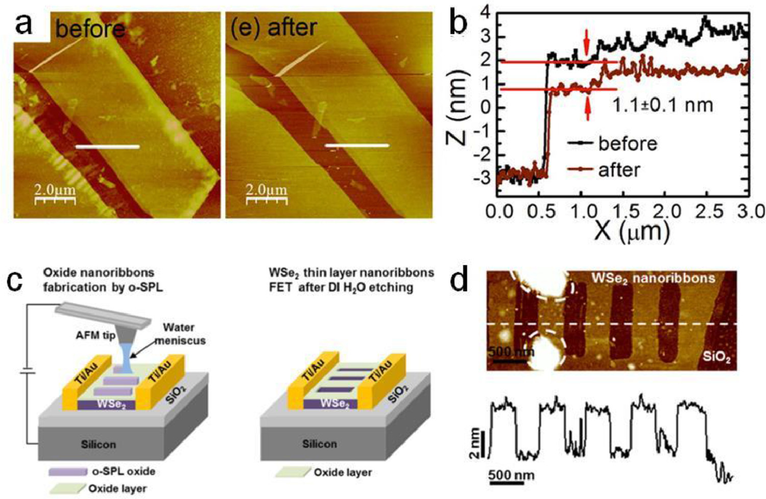
| Fig. 6. (a) AFM images and (b) line profiles measured on MoS2 flakes before and after the self-limiting oxidation and annealing. Reprinted with permission [95]. Copyright 2016, American Chemical Society. (c) Schematic showing the fabrication of WSe2 nanoribbon using the oxidation scanning probe lithography followed by H2O etching. (d) The AFM image and line profile of the fabricated nanoribbons. Reprinted with permission [99]. Copyright 2018, American Chemical Society. | |
By spatially inducing and controlling the oxidation by applying local voltages using scanning probe, patterning 2D semiconductors into complex geometries can also be realized. This technique has been initially employed to pattern graphene with nanoscale resolutions [101, 102]. Controlled patterning of BP has been demonstrated with nanoscale spatial resolution using conductive atomic force microscopy [103]. The patterning is due to the anodic oxidation, which is verified by the formation of oxidized phosphorus species. The oxidized phosphorus is water soluble and therefore can be easily removed by water rinsing. Similar work has also been done for WSe2, where oxidation was induced in the designed ribbon-shapes with controlled width and depth by oxidation scanning probe lithography [99]. By the removal of the oxides by water, the WSe2 nanoribbons are therefore produced (Figs. 6c and d).
4.2. Material modificationDoping is a primary technique to tune the transport in semiconductor-based field effect transistors (FET). For thin films, ion implantation and thermal diffusion are the commonly adopted techniques to control the carrier type and carrier concentrations in semiconductors. However, they are not compatible with 2D semiconductors as the 2D crystalline cannot survive the process. Element substitute during the synthesis is a way to dope 2D semiconductors [104].
For example, using niobium substitution of molybdenum atoms during the growth of MoS2 can change the intrinsic n-type characteristic to p-type behavior [105, 106]. Beyond traditional substitutional doping, surface doping plays a significant role in 2D semiconductors due to their atomically-thin nature [107-109]. Controlled doping to 2D semiconductors can be induced by surface oxidation under certain circumstances. Surface oxides MoOx and WOx (x < 3) formed on the surface of molybdenum and tungsten chalcogenides possess high work functions of 6.6 eV and 6.3 eV, respectively, which are inside the valence bands of all molybdenum and tungsten chalcogenides [110, 111]. Hence, surface oxidation can be used to induce effective p-doping to the underlying TMDs. This surface modification charge transfer doping technique has been shown to be more advantageous for FET applications due to enhanced control on doping. In the previous section, we introduced that the oxygen plasma and ozone treatment induced oxidation is a self-limited layer-by-layer process. The fully oxidized surface could effectively prevent the vertical diffusion of oxygen into the underlying layers to create further charged defects, which are highly undesired as they significantly reduce the mobility, increase the sub-threshold swing slope, and cause hysteresis and long-term drifts in the transfer characteristics. These treatments are also compatible to the conventional semiconductor processing techniques, making them promising for future applications in the next-generation electronics.
By carefully controlling the plasma power and treatment durations, the controlled p-doping have been demonstrated in the intrinsic n-type WSe2 and MoTe2 using plasma and ozone induced layer-by-layer oxidation [84, 97, 98, 112-114]. Moreover, the plasma treatment produces more firm oxide layer than ozone treatment, which exhibits robust p-doping characteristics even after the long storage in air ambient or short soaking in organic solutions [84, 98]. Furthermore, the spatial control on the doping area is expected by using capping masks to protect the designated area from oxidation [77]. Complex structures such as p-n junctions therefore can be fabricated using the oxidation induced doping.
Electrical contact is another big concern when building 2D FETs. Normally, the electronic device of 2D semiconductors are suffered from the large contact resistance which originates from the Schottky barrier formed at the contact interface as a result of poor band alignment or Fermi-level pinning because of the massive disorders induced in 2D semiconductors during metal deposition [115].
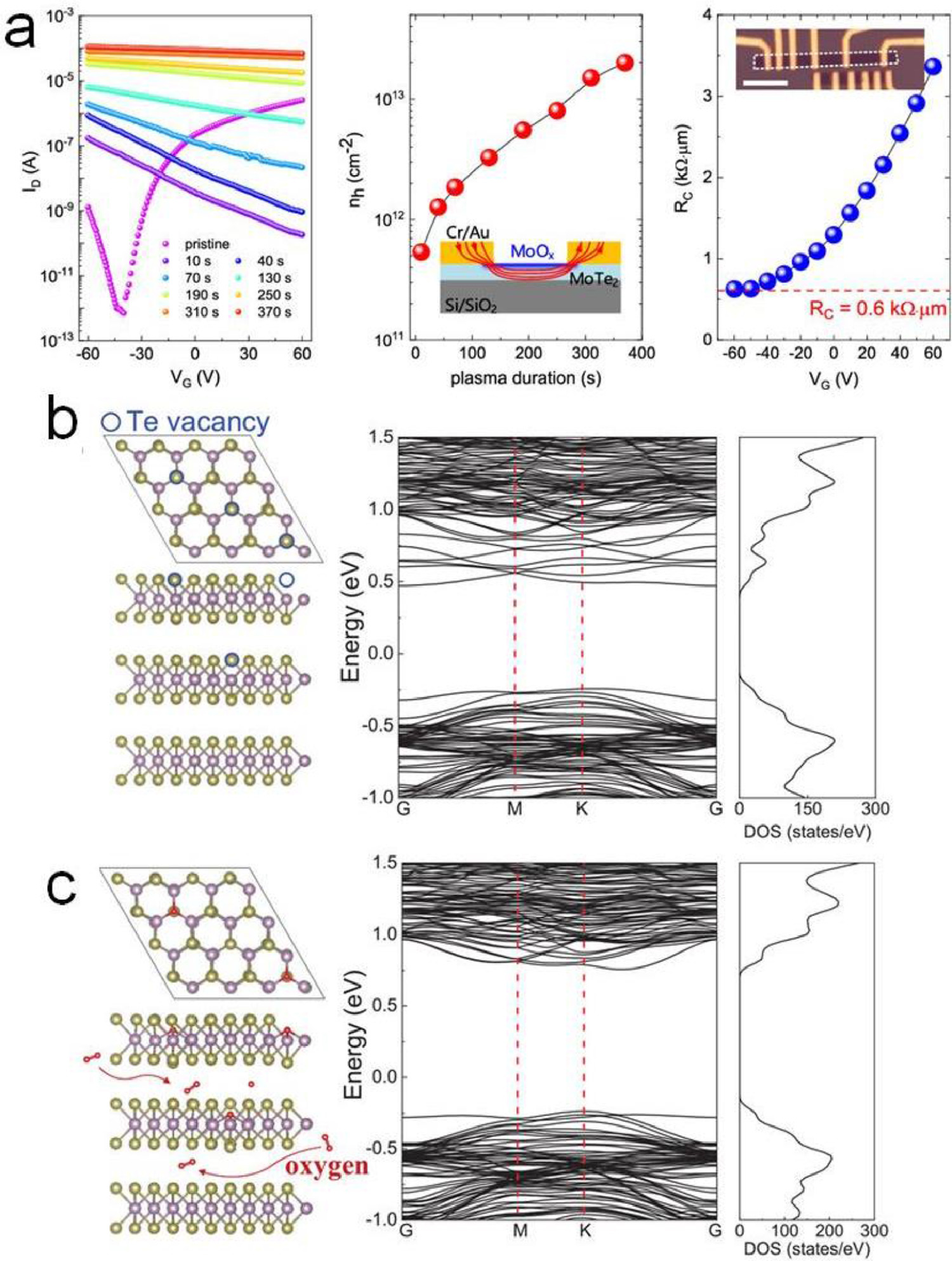
Using the degenerately doped materials as electric contacts, the contact resistance of the device can be significantly reduced, which is widely employed in the complementary metal-oxide-semiconductor (CMOS) technology. Degenerate hole doping to MoTe2 has been demonstrated by using room temperature oxygen plasma treatment (Fig. 7a) [84]. When the topmost layer is fully oxidized, the hole concentration can reach 2 × 1013 cm−2 without additional gate modulation. Using it as the contacts, an extremely low contact resistance of 0.6 kΩ µm is achieved.

|
Download:
|
| Fig. 7. (a) Transfer characteristics of a MoTe2 FET subjected to the O2 plasma treatments with varied durations and the extracted hole-sheet density. Contact resistance measured with the transmission line model device for the MoTe2 subjected a long plasma treatment. Reprinted with permission [84]. Copyright 2020, American Chemical Society. Atomic crystal structure and electronic band structure of (c) defective trilayer MoTe2 with one Te monovacancy in each layer highlighted by blue circles and (d) selectively oxidized MoTe2 at the vacancies by the intercalated oxygen. Reprinted with permission [117]. Copyright 2020, Wiley-VCH GmbH. | |
Defects formed inside the 2D semiconductors also degrade the performance of their FETs. As aforementioned, tellurides have a low structural stability and are prone to create Te vacancies. For instance, Te vacancies are able to induce extra mid-gap charged states near the conduction band minimum of MoTe2 (Fig. 7b) [116]. Processes such as baking and electron irradiations during the device fabrication can aggravate the formation of defects and therefore degrade the performance of its FET. Controlled Low pressure oxygen annealing has been utilized to induce oxygen intercalation in MoTe2. The intercalated oxygen selectively oxidizes at Te vacancies where the activation energy is low, and leaves other part of MoTe2 untouched [117]. This weak oxidation has been varied to be able to remove charged states (Fig. 7c) and restore the electronic properties of MoTe2, for example, a high hole current density exceeding 20 µA/µm, a record high hole mobility of 77 cm2 V−1 s−1 (Fig. 7b).
Other than the electronic properties, controlled oxidation has also been demonstrated to enhance the PL emission for transition metal dichalcogenides. Firstly, a unique property of TMDs known as the indirect-to-direct band gap transition when these materials change from bulk to a monolayer flake. Subsequently, the photoluminescence intensity drastically increases with the decreased number of layers. Using oxygen plasma, the significant enhancements of PL intensity have been observed in the treated bilayer MoS2, MoSe2, and WSe2, in which the topmost layer is oxidized leaving only one active TMD layer [94, 118]. Besides the band structure modulation due to the materials thinning, the increased bound exciton emission can also lead to enhanced PL signal. The much enhanced PL intensities were detected in monolayer MoS2 locally near the oxidized defects and in the MoS2 and WSe2 with surface oxides induced by controlled layer-by-layer oxidation process [119, 120], as the Mo-O or W-O bonds lead to the saturation of traps and increased radiative recombination rates. However, special attention should be paid when tuning PL with oxidations, as the uncontrolled harsh oxidation, which is responsible to the severe mid-gap states or non-radiative recombination centers, has been reported to quenches PL emissions largely, e.g., in MoS2 [121] and WS2 [36].
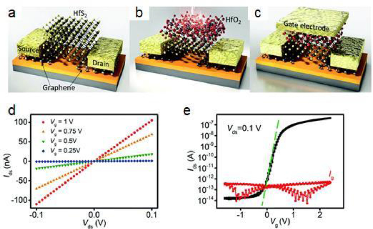
4.3. Dielectric synthesisThe success of silicon in the modern information technology in some aspect can be ascribed to the its nature oxide silicon dioxide, which acts as dielectric layer in its electronic devices with an excellent interface quality. 2D semiconductor based nanoelectronic devices are far from their full theoretically predicted performance due to the lack of compatible dielectrics [122]. The deposited oxides that widely employed in thin film process offer poorly defined interface on 2D semiconductors and deteriorate the device performance [122]. Drawing on the experience of silicon, the use of nature oxides of 2D semiconductors as dielectric layer for 2D device seems a promising way. In the early stage of the research, there are only a few reports on using surface native oxide or the oxidized 2D semiconductors as the dialectics for the 2D electronic device. Mleczko et al. demonstrated the possibility of naturally oxidizing HfSe2 and ZrSe2 to synthesize native high-k oxides HfO2 and ZrO2. Then Lai et al. reported a top-gated HfS2 field effect transistor using the surface oxide HfO2 as gate dielectric, which is analogous to the Si/SiO2 heterostructure in the silicon based FETs (Fig. 8) [123]. The surface oxidation was induced by oxygen plasma treatment, with which the oxidation was verified to be a layer-by-layer process. This ensures a high interface quality with low interface trap density of 1011 cm−2 eV−1, which is about 1~2 orders of magnitude lower than that in the deposited HfO2 thin-film [124, 125]. Hence, they demonstrated a high device performance with the sub-threshold swing slope as low as 67 mV/dec. More recently, Peimyoo et al. reported the selective photo-oxidation of HfS2 into an amorphous HfOx inside vdW heterostructures using laser irradiation [126]. Based on that, they demonstrated a variety of device functionalities, including FET, memory device, and optoelectronic device. Plasma induced oxide POx layer on the surface of BP has also been utilized as dielectric to realize FET device function [127]. In addition, Ta2O5 synthesized by thermally oxidizing TaS2 has been transferred onto MoS2 as a high-k gate dielectric to realize FET with low SS of 61 mV/dec [128]. In many cases, the resulted oxide dielectrics are nonstoichiometric therefore contain high defect densities and limited dielectric strength. Overall, this field is relatively new, which requires further and systematic exploration.

|
Download:
|
| Fig. 8. (a–c) Schematic diagrams of the process for the fabrication of a top-gated FET based on the converted HfO2/HfS2 hybrid structure. (d, e) Output and transfer characteristics of the top gated HfS2 FET with oxidized surface HfO2 dielectric. Reprinted with permission [123]. Copyright 2018, The Royal Society of Chemistry. | |
The chemical stability of 2D semiconductors in ambient is of great importance to their fundamental properties and their technological applications. In this review, we discussed the fundamentals of the ambient oxidation of some representative 2D semiconductors, including BP, transition metal dichalcogenides and transition metal monochalcogenides. Theoretical calculations combined with multiple characterization techniques, e.g., AFM, Raman spectroscopy, XPS, TEM, have been utilized in order to establish the whole picture of the oxidation mechanism for various materials. The roles of the key factors of the ambient oxidations, i.e., oxygen, water, heat and light illumination, have been summarized. In most of the cases, especially for these transition metal dichalcogenides and transition metal monochalcogenides with high activation energies, the intrinsic materials with no defects are found to be chemically stable in air. In practice, their highly reactive properties are ascribed to the inevitably possessed defects and light illumination. Many efforts have been dedicated to the development of feasible methods to passivate the reactive surface. Appropriate passivation could potentially prolong the lifetime of 2D semiconductors in ambient from few hours to nearly a year. Physical capping including the self-passivation by the surface oxides, and chemical surface functionalization are the two commonly employed techniques. So far, the h-BN encapsulation seems the most reliable and stable passivation in the lab. However, as the development of 2D semiconductors goes further, the passivation facing the mass production must be developed, which is most likely to be a chemical passivation technique, which should be relatively stable and provides no significant change to the passivated semiconductors. In the end, we concluded the recent progress of applications of the controlled oxidations using various techniques in 2D semiconductors patterning, modification, and synthesis. In particular, the use of native oxides of 2D semiconductors, such as HfSe2 and HfS2, seems a promising way to have 2D compatible high-k dielectric while they offer improved interface quality with 2D semiconductors. Nevertheless, under most of the circumstances the resulted nonstoichiometric oxides are expected to exhibit very high defects which limit their dielectric characteristics. And the performance of these 2D oxide as dielectric for varied applications are currently unknown. We hope that this review will inspire further investigations on the oxidations of novel 2D semiconductors in ambient and particularly stimulate more potential applications by utilizing the controlled oxidations in 2D semiconductors.
Declaration of competing interestWe declare that we do not have any commercial or associative interest that represents a conflict of interest in connection with the work submitted.
AcknowledgmentsThis work was partially supported by the National Natural Science Foundation of China (No. 11804397), the Hunan High-Level Talent Program (No. 2019RS1006).
| [1] |
M.L. Chen, X. Sun, H. Liu, et al., Nat. Commun. 11 (2020) 1205. DOI:10.1038/s41467-020-15096-0 |
| [2] |
C. Liu, H. Chen, S. Wang, et al., Nat. Nanotechnol. 15 (2020) 545-557. DOI:10.1038/s41565-020-0724-3 |
| [3] |
H. Li, J.K. Huang, Y. Shi, et al., Adv. Mater. Interfaces 6 (2019) 1900220. DOI:10.1002/admi.201900220 |
| [4] |
S. Manzeli, D. Ovchinnikov, D. Pasquier, O. Yazyev, A. Kis, Nat. Rev. Mater. 2 (2017) 17033. DOI:10.1038/natrevmats.2017.33 |
| [5] |
S. Zhao, B. Dong, H. Wang, et al., Nanoscale Adv. 2 (2020) 109-139. DOI:10.1039/c9na00623k |
| [6] |
J. Sun, R.S. Deacon, W. Luo, et al., Commun. Phys. 3 (2020) 93. DOI:10.1038/s42005-020-0357-8 |
| [7] |
X. Liu, Y. Yuan, Z. Wang, et al., Phys. Rev. Appl. 13 (2020) 044056. DOI:10.1103/PhysRevApplied.13.044056 |
| [8] |
Y. Liu, X. Duan, H.J. Shin, et al., Nature 591 (2021) 43-53. DOI:10.1038/s41586-021-03339-z |
| [9] |
M. Chhowalla, D. Jena, H. Zhang, Nat. Rev. Mater. 1 (2016) 16052. DOI:10.1038/natrevmats.2016.52 |
| [10] |
J. Sun, M. Muruganathan, H. Mizuta, Sci. Adv. 2 (2016) e1501518. DOI:10.1126/sciadv.1501518 |
| [11] |
M. Muruganathan, J. Sun, T. Imamura, H. Mizuta, Nano Lett. 15 (2015) 8176-8180. DOI:10.1021/acs.nanolett.5b03653 |
| [12] |
Z. Wang, Q. Jingjing, X. Wang, et al., Chem. Soc. Rev. 47 (2018) 6128-6174. |
| [13] |
S. Bertolazzi, P. Bondavalli, S. Roche, et al., Adv. Mater. 31 (2019) 1806663. DOI:10.1002/adma.201806663 |
| [14] |
X. Liu, X. Zhou, Y. Pan, et al., Adv. Mater. 32 (2020) 2004813. DOI:10.1002/adma.202004813 |
| [15] |
J. Sun, M.E. Schmidt, M. Muruganathan, H. Chong, H. Mizuta, Nanoscale 8 (2016) 6659-6665. DOI:10.1039/C6NR00253F |
| [16] |
J. Sun, W. Wang, M. Muruganathan, H. Mizuta, Appl. Phys. Lett. 105 (2014) 033103. DOI:10.1063/1.4891055 |
| [17] |
J. Mei, T. Liao, L. Kou, Z. Sun, Adv. Mater. 29 (2017) 1700176. DOI:10.1002/adma.201700176 |
| [18] |
W. Bi, C. Wu, Y. Xie, ACS Energy Lett. 3 (2018) 624-633. DOI:10.1021/acsenergylett.7b01343 |
| [19] |
X. Wang, Y. Sun, K. Liu, 2D Mater. 6 (2019) 042001. DOI:10.1088/2053-1583/ab20d6 |
| [20] |
V. Tran, R. Soklaski, Y. Liang, L. Yang, Phys. Rev. B 89 (2014) 235319. DOI:10.1103/PhysRevB.89.235319 |
| [21] |
A. Ziletti, A. Carvalho, D.K. Campbell, D.F. Coker, A.H. Castro, Phys. Rev. Lett. 114 (2015) 046801. DOI:10.1103/PhysRevLett.114.046801 |
| [22] |
J.D. Wood, S.A. Wells, D. Jariwala, et al., Nano Lett. 14 (2014) 6964-6970. DOI:10.1021/nl5032293 |
| [23] |
Y. Huang, J. Qiao, K. He, et al., Chem. Mater. 28 (2016) 8330-8339. DOI:10.1021/acs.chemmater.6b03592 |
| [24] |
A. Favron, E. Gaufres, F. Fossard, et al., Nat. Mater. 14 (2015) 826-832. DOI:10.1038/nmat4299 |
| [25] |
T. Ahmed, S. Balendhran, M.N. Karim, et al., NPJ 2D Mater. Appl. 1 (2017) 18. DOI:10.1038/s41699-017-0023-5 |
| [26] |
S. Walia, Y. Sabri, T. Ahmed, et al., 2D Mater. 4 (2016) 015025. DOI:10.1088/2053-1583/4/1/015025 |
| [27] |
A.E. Naclerio, D.N. Zakharov, J. Kumar, et al., ACS Appl. Mater. Interfaces 12 (2020) 15844-15854. DOI:10.1021/acsami.9b21116 |
| [28] |
K.H. Oh, S.W. Jung, K.S. Kim, Appl. Surf. Sci. 504 (2020) 144341. DOI:10.1016/j.apsusc.2019.144341 |
| [29] |
G. Mirabelli, C. McGeough, M. Schmidt, et al., J. Appl. Phys. 120 (2016) 125102. DOI:10.1063/1.4963290 |
| [30] |
S. KC, R.C. Longo, R.M. Wallace, K. Cho, J. Appl. Phys. 117 (2015) 135301. DOI:10.1063/1.4916536 |
| [31] |
P. Budania, P. Baine, J. Montgomery, et al., MRS Commun. 7 (2017) 813-818. DOI:10.1557/mrc.2017.105 |
| [32] |
R.C. Longo, R. Addou, S. KC, et al., 2D Mater. 4 (2017) 025050. DOI:10.1088/2053-1583/aa636c |
| [33] |
S.S. Grønborg, K. Thorarinsdottir, L. Kyhl, et al., 2D Mater. 6 (2019) 045013. DOI:10.1088/2053-1583/ab2d00 |
| [34] |
H. Liu, N. Han, J. Zhao, RSC Adv. 5 (2015) 17572-17581. DOI:10.1039/C4RA17320A |
| [35] |
X. Zhang, F. Jia, B. Yang, S. Song, J. Phys. Chem. C 121 (2017) 9938-9943. DOI:10.1021/acs.jpcc.7b01863 |
| [36] |
J. Gao, B. Li, J. Tan, P. Chow, T. Lu, N. Koratkar, ACS Nano 10 (2016) 2628-2635. DOI:10.1021/acsnano.5b07677 |
| [37] |
Y. Liu, C. Tan, H. Chou, et al., Nano Lett. 15 (2015) 4979-4984. DOI:10.1021/acs.nanolett.5b02069 |
| [38] |
J.C. Kotsakidis, Q. Zhang, A.L. Vazquez de Parga, et al., Nano Lett. 19 (2019) 5205-5215. DOI:10.1021/acs.nanolett.9b01599 |
| [39] |
J.H. Park, S. Vishwanath, X. Liu, et al., ACS Nano 10 (2016) 4258-4267. DOI:10.1021/acsnano.5b07698 |
| [40] |
H. Zhu, Q. Wang, L. Cheng, et al., ACS Nano 11 (2017) 11005-11014. DOI:10.1021/acsnano.7b04984 |
| [41] |
C. Si, D. Choe, W. Xie, et al., Nano Lett. 19 (2019) 3612-3617. DOI:10.1021/acs.nanolett.9b00613 |
| [42] |
L. Muechler, W. Hu, L. Lin, C. Yang, R. Car, Phys. Rev. B 102 (2020) 041103. |
| [43] |
F. Ye, J. Lee, J. Hu, et al., Small 12 (2016) 5802-5808. DOI:10.1002/smll.201601207 |
| [44] |
H.C. Diaz, R. Chaghi, Y. Ma, M. Batzill, 2D Mater. 2 (2015) 044010. DOI:10.1088/2053-1583/2/4/044010 |
| [45] |
F. Hou, D. Zhang, P. Sharma, et al., ACS Appl. Electron. Mater. 2 (2020) 2196-2202. DOI:10.1021/acsaelm.0c00380 |
| [46] |
S.H. Chae, Y. Jin, T.S. Kim, et al., ACS Nano 10 (2016) 1309-1316. DOI:10.1021/acsnano.5b06680 |
| [47] |
S. Mañas-Valero, V. García-López, A. Cantarero, M. Galbiati, Appl. Sci. 6 (2016) 264. DOI:10.3390/app6090264 |
| [48] |
Q. Yao, L. Zhang, P. Bampoulis, H.J.W. Zandvliet, J. Phys. Chem. C 122 (2018) 25498-25505. DOI:10.1021/acs.jpcc.8b08713 |
| [49] |
A. Cruz, Z. Mutlu, M. Ozkan, et al., MRS Commun. 8 (2018) 1191-1196. DOI:10.1557/mrc.2018.185 |
| [50] |
M.J. Mleczko, C. Zhang, H.R. Lee, et al., Sci. Adv. 3 (2017) e1700481. DOI:10.1126/sciadv.1700481 |
| [51] |
Y. Guo, S. Zhou, Y. Bai, J. Zhao, ACS Appl. Mater. Interfaces 9 (2017) 12013-12020. DOI:10.1021/acsami.6b16786 |
| [52] |
Y.K. Lee, Z. Luo, S.P. Cho, M.G. Kanatzidis, I. Chung, Joule 3 (2019) 719-731. DOI:10.1016/j.joule.2019.01.001 |
| [53] |
E. Sutter, B. Zhang, M. Sun, et al., ACS Nano 13 (2019) 9352-9362. DOI:10.1021/acsnano.9b03986 |
| [54] |
L.C. Gomes, A. Carvalho, A.C. Neto, Phys. Rev. B 94 (2016) 054103. DOI:10.1103/PhysRevB.94.054103 |
| [55] |
S. Barraza-Lopez, T.P. Kaloni, ACS Cent. Sci. 4 (2018) 1436-1446. DOI:10.1021/acscentsci.8b00589 |
| [56] |
D.J. Late, B. Liu, J. Luo, et al., Adv. Mater. 24 (2012) 3549-3554. DOI:10.1002/adma.201201361 |
| [57] |
P.H. Ho, Y.R. Chang, Y.C. Chu, et al., ACS Nano 11 (2017) 7362-7370. DOI:10.1021/acsnano.7b03531 |
| [58] |
M. Rahaman, R.D. Rodriguez, M. Monecke, S.A. Lopez-Rivera, D.R.T. Zahn, Semicond. Sci. Technol. 32 (2017) 105004. DOI:10.1088/1361-6641/aa8441 |
| [59] |
T.E. Beechem, B.M. Kowalski, M.T. Brumbach, et al., Appl. Phys. Lett. 107 (2015) 173103. DOI:10.1063/1.4934592 |
| [60] |
A. Bergeron, J. Ibrahim, R. Leonelli, et al., Appl. Phys. Lett. 110 (2017) 241901. DOI:10.1063/1.4986189 |
| [61] |
Y. Liu, P. Stradins, S.H. Wei, Angew. Chem. Int. Ed. 55 (2016) 965-968. DOI:10.1002/anie.201508828 |
| [62] |
L. Shi, Q. Zhou, Y. Zhao, et al., J. Phys. Chem. Lett. 8 (2017) 4368-4373. DOI:10.1021/acs.jpclett.7b02059 |
| [63] |
Y. Guo, S. Zhou, Y. Bai, J. Zhao, J. Chem. Phys. 147 (2017) 104709. DOI:10.1063/1.4993639 |
| [64] |
L. Shi, Q. Li, Y. Ouyang, J. Wang, Nanoscale 10 (2018) 12180-12186. DOI:10.1039/C8NR01533C |
| [65] |
M. Kang, S. Rathi, I. Lee, et al., Appl. Phys. Lett. 106 (2015) 143108. DOI:10.1063/1.4917458 |
| [66] |
F. Alsaffar, S. Alodan, A. Alrasheed, et al., Sci. Rep. 7 (2017) 44540. DOI:10.1038/srep44540 |
| [67] |
X. Luo, Y. Rahbarihagh, J.C. Hwang, et al., IEEE Electron. Device Lett. 35 (2014) 1314-1316. DOI:10.1109/LED.2014.2362841 |
| [68] |
T. Kanazawa, T. Amemiya, V. Upadhyaya, et al., Proceedings of the 16th International Conference Nanotechnology, 2016, pp. 865–867.
|
| [69] |
R. Galceran, E. Gaufres, A. Loiseau, et al., Appl. Phys. Lett. 111 (2017) 243101. DOI:10.1063/1.5008484 |
| [70] |
N. Lee, H. Jeon, J ECS, Solid State Sci. Technol. 10 (2021) 023001. DOI:10.1149/2162-8777/abddd7 |
| [71] |
H. Liu, K. Xu, X. Zhang, et al., Appl. Phys. Lett. 100 (2012) 152115. DOI:10.1063/1.3703595 |
| [72] |
W. Li, J. Zhou, S. Cai, et al., Nat. Electron. 2 (2019) 563-571. DOI:10.1038/s41928-019-0334-y |
| [73] |
T. Nam, S. Seo, H. Kim, J. Vac. Sci. Technol. A 38 (2020) 030803. DOI:10.1116/6.0000068 |
| [74] |
L. Cheng, X. Qin, A.T. Lucero, et al., ACS Appl. Mater. Interfaces 6 (2014) 11834-11838. DOI:10.1021/am5032105 |
| [75] |
J.H. Park, S. Fathipour, I. Kwak, K. Sardashti, A.C. Kummel, ACS Nano 10 (2016) 6888-6896. DOI:10.1021/acsnano.6b02648 |
| [76] |
H. Zhu, R. Addou, Q. Wang, et al., Nanotechnology 31 (2019) 055704. |
| [77] |
X. Liu, Y. Yuan, D. Qu, et al., Phys. Status Solidi RRL 13 (2019) 1900208. DOI:10.1002/pssr.201900208 |
| [78] |
A.J. Cho, J.Y. Kwon, ACS Appl. Mater. Interfaces 11 (2019) 39765-39771. DOI:10.1021/acsami.9b11219 |
| [79] |
X. Chen, Y. Wu, Z. Wu, et al., Nat. Commun. 6 (2015) 7315. DOI:10.1038/ncomms8315 |
| [80] |
D. Yue, D. Lee, Y.D. Jang, et al., Nanoscale 8 (2016) 12773-12779. DOI:10.1039/C6NR02554D |
| [81] |
G. Long, D. Maryenko, J. Shen, et al., Nano Lett. (2016) 7768-7773. DOI:10.1021/acs.nanolett.6b03951 |
| [82] |
H. Arora, Y. Jung, T. Venanzi, et al., ACS Appl. Mater. Interfaces 11 (2019) 43480-43487. DOI:10.1021/acsami.9b13442 |
| [83] |
J. Holler, L. Bauriedl, T. Korn, et al., 2D Mater. 7 (2019) 015012. |
| [84] |
X. Liu, D. Qu, Y. Yuan, et al., ACS Appl. Mater. Interfaces 12 (2020) 26586-26592. DOI:10.1021/acsami.0c03762 |
| [85] |
N. Higashitarumizu, H. Kawamoto, M. Nakamura, et al., Nanoscale 10 (2018) 22474-22483. DOI:10.1039/c8nr06390g |
| [86] |
C.R. Ryder, J.D. Wood, S.A. Wells, et al., Nat. Chem. 8 (2016) 597-602. DOI:10.1038/nchem.2505 |
| [87] |
S. Walia, S. Balendhran, T. Ahmed, et al., Adv. Mater. 29 (2017) 1700152. DOI:10.1002/adma.201700152 |
| [88] |
C. Su, Z. Yin, Q.B. Yan, et al., Proc. Natl. Acad. Sci. U. S. A. 116 (2019) 20844-20849. DOI:10.1073/pnas.1909500116 |
| [89] |
J.H. Park, A. Sanne, Y. Guo, et al., Sci. Adv. 3 (2017) e1701661. DOI:10.1126/sciadv.1701661 |
| [90] |
X. Xu, Z. Chen, B. Sun, et al., Sci. Bull. 64 (2019) 1700-1706. DOI:10.1016/j.scib.2019.09.009 |
| [91] |
K. Cho, J. Pak, S. Chung, T. Lee, ACS Nano 13 (2019) 9713-9734. DOI:10.1021/acsnano.9b02540 |
| [92] |
X. Duan, C. Wang, A. Pan, R. Yu, X. Duan, Chem. Soc. Rev. 44 (2015) 8859-8876. DOI:10.1039/C5CS00507H |
| [93] |
J. Gusakova, X. Wang, L.L. Shiau, et al., Phys. Status Solidi a 214 (2017) 1700218. DOI:10.1002/pssa.201700218 |
| [94] |
Z. Li, S. Yang, R. Dhall, et al., ACS Nano 10 (2016) 6836-6842. DOI:10.1021/acsnano.6b02488 |
| [95] |
H. Zhu, X. Qin, L. Cheng, A. Azcatl, R.M. Wallace, ACS Appl. Mater. Interfaces 8 (2016) 19119-19126. DOI:10.1021/acsami.6b04719 |
| [96] |
Q. Wang, J. Chen, Y. Zhang, et al., Nanomaterials 9 (2019) 756. DOI:10.3390/nano9050756 |
| [97] |
X. Zheng, Y. Wei, C. Deng, et al., ACS Appl. Mater. Interfaces 10 (2018) 30045-30050. DOI:10.1021/acsami.8b11003 |
| [98] |
M. Yamamoto, S. Dutta, S. Aikawa, et al., Nano Lett. 15 (2015) 2067-2073. DOI:10.1021/nl5049753 |
| [99] |
A.I. Dago, Y. Ryu, F.J. Palomares, et al., ACS Appl. Mater. Interfaces 10 (2018) 40054-40061. DOI:10.1021/acsami.8b15937 |
| [100] |
S.S. Wu, T.X. Huang, K.Q. Lin, et al., 2D Mater. 6 (2019) 045052. DOI:10.1088/2053-1583/ab42b6 |
| [101] |
I.-S. Byun, D. Yoon, J.S. Choi, et al., ACS Nano 5 (2011) 6417-6424. DOI:10.1021/nn201601m |
| [102] |
S. Masubuchi, M. Arai, T. Machida, Nano Lett. 11 (2011) 4542-4546. DOI:10.1021/nl201448q |
| [103] |
X. Liu, K.S. Chen, S.A. Wells, et al., Adv. Mater. 29 (2017) 1604121. DOI:10.1002/adma.201604121 |
| [104] |
L. Loh, Z. Zhang, M. Bosman, G. Eda, Nano Res. 14 (2021) 1668-1681. DOI:10.1007/s12274-020-3013-4 |
| [105] |
J. Suh, T.E. Park, D.Y. Lin, et al., Nano Lett. 14 (2014) 6976-6982. DOI:10.1021/nl503251h |
| [106] |
J. Suh, T.L. Tan, W. Zhao, et al., Nat. Commun. 9 (2018) 199. DOI:10.1038/s41467-017-02631-9 |
| [107] |
Y. Wang, Y. Zheng, C. Han, et al., Nano Res. 14 (2021) 1682-1697. DOI:10.1007/s12274-020-2919-1 |
| [108] |
Z. Wang, Y. Yuan, X. Liu, et al., ACS Nano 13 (2019) 7502-7507. DOI:10.1021/acsnano.9b02935 |
| [109] |
Z. Wang, J. Sun, M. Muruganathan, H. Mizuta, Appl. Phys. Lett. 113 (2018) 133101. DOI:10.1063/1.5042696 |
| [110] |
I. Moon, S. Lee, M. Lee, et al., Nanoscale 11 (2019) 17368-17375. DOI:10.1039/c9nr05881h |
| [111] |
S. Chuang, C. Battaglia, A. Azcatl, et al., Nano Lett. 14 (2012) 1337-1342. |
| [112] |
P.R. Pudasaini, A. Oyedele, C. Zhang, et al., Nano Res. 11 (2018) 722-730. DOI:10.1007/s12274-017-1681-5 |
| [113] |
A.N. Hoffman, M.G. Stanford, M.G. Sales, et al., 2D Mater. 6 (2019) 045024. DOI:10.1088/2053-1583/ab2fa7 |
| [114] |
M. Yamamoto, S. Nakaharai, K. Ueno, et al., Nano Lett. 16 (2016) 2720-2727. DOI:10.1021/acs.nanolett.6b00390 |
| [115] |
A. Allain, J. Kang, K. Banerjee, A. Kis, Nat. Mater. 14 (2015) 1195-1205. DOI:10.1038/nmat4452 |
| [116] |
S. Haldar, H. Vovusha, M.K. Yadav, O. Eriksson, B. Sanyal, Phys. Rev. B 92 (2015) 235408. DOI:10.1103/PhysRevB.92.235408 |
| [117] |
X. Liu, D. Qu, L. Wang, et al., Adv. Funct. Mater. 30 (2020) 2004880. DOI:10.1002/adfm.202004880 |
| [118] |
S. Kang, Y.S. Kim, J.H. Jeong, et al., ACS Appl. Mater. Interfaces 13 (2021) 1245-1252. DOI:10.1021/acsami.0c18364 |
| [119] |
H. Nan, Z. Wang, W. Wang, et al., ACS Nano 8 (2014) 5738-5745. DOI:10.1021/nn500532f |
| [120] |
T.F.D. Fernandes, A. de C. Gadelha, A.P.M. Barboza, 2D Mater. 5 (2018) 025018. DOI:10.1088/2053-1583/aab38c |
| [121] |
N. Kang, H.P. Paudel, M.N. Leuenberger, L. Tetard, S.I. Khondaker, J. Phys. Chem. C 118 (2014) 21258-21263. DOI:10.1021/jp506964m |
| [122] |
Y.Y. Illarionov, T. Knobloch, M. Jech, et al., Nat. Commun. 11 (2020) 3385. DOI:10.1038/s41467-020-16640-8 |
| [123] |
S. Lai, S. Byeon, S.K. Jang, et al., Nanoscale 10 (2018) 18758-18766. DOI:10.1039/c8nr06020g |
| [124] |
K. Xu, Y. Huang, B. Chen, et al., Small 12 (2016) 3106-3111. DOI:10.1002/smll.201600521 |
| [125] |
X. Zou, J. Wang, C.H. Chiu, et al., Adv. Mater. 26 (2014) 6255-6261. DOI:10.1002/adma.201402008 |
| [126] |
N. Peimyoo, M. Barnes, J. Mehew, et al., Sci. Adv. 5 (2019) eaau0906. |
| [127] |
W. Dickerson, V. Tayari, I. Fakih, et al., Appl. Phys. Lett. 112 (2018) 173101. DOI:10.1063/1.5011424 |
| [128] |
B. Chamlagain, Q. Cui, S. Paudel, et al., 2D Mater. 4 (2017) 031002. DOI:10.1088/2053-1583/aa780e |