 2022, Vol. 33


b International Center for Young Scientists (ICYS), National Institute for Materials Science (NIMS), Tsukuba 305-0044, Japan;
c Shenzhen Research Institute, City University of Hong Kong, Shenzhen 518057, China
Two-dimensional (2D) transition metal dichalcogenide (TMD) nanosheets have become a hot research topic in recent years due to its diverse properties [1-7], such as topological insulator properties [8, 9], superconductivity [10, 11], valley polarization [12, 13] and enhanced catalytic activity for various chemical reactions [14-21]. Particularly, the atomically thin body and dangling-bond free surface of 2D TMD materials make them promising channel materials for high-performance field-effect transistors (FETs) [22-24]. The bulk TMDs are actually a family of materials widely studied since 1960s with various properties [25]. They are presented as MX2, where M is the transition metal in Group 4 to Group 10 and X represents the chalcogen elements of S, Se or Te, which can crystallize in non-layer structure or graphite-like layered structure (mainly the Groups 4–7 TMDs). Typically, recent advances in sample preparation have boosted a great development of 2D layered TMD nanosheets, which not only inherit most properties of their bulk counterparts, but also present unique layer-dependent characteristics due to the electron confinement effects [26, 27]. Therefore, the preparation of 2D TMD nanosheets provides a new platform for both discovering new physical phenomena and enabling breakthrough in a variety of fields like materials science, chemistry and nanotechnology [1-7].
To further explore the potential of 2D TMD nanosheets, many compelling strategies like vacancies engineering, heteroatom doping and introducing second component into/onto 2D TMD nanosheets were put forward to tune their properties [17, 28-32]. More recently, the alloying of different 2D TMD nanosheets has emerged as an effective approach to implement such modulation mechanism [33, 34]. In 2D alloyed TMD nanosheets, one of the elements in binary TMD can be substituted by another element at an arbitrary percentage while the crystal structure remaining in a single homogeneous phase, and many 2D alloyed TMD nanosheets with miscible chalcogens (e.g., MoS2(1-x)Se2x, WS2(1-x)Se2x, ReS2(1-x)Se2x and WSe2(1-x)Te2x), or miscible transition metals (e.g., MoxW1-xS2, MoxRe1-xS2, W1-xNbxS2 and V1-xTaxS2) have been well-prepared with tunable composition [35-42]. Given the diverse properties of 2D TMD nanosheets, the alloying technology offers further opportunity to fine-tune their properties, e.g., bandgap/band position, charge carrier type, vibrational frequency and lattice parameter. Moreover, it shows the possibility of obtaining materials with not only enhanced electrical, optical and catalytic performance but new properties, such as magnetism [43-45]. To date, 2D alloyed TMD nanosheets can be prepared by those well-developed methods for 2D TMDs, such as exfoliation of chemical vapor transport (CVT)-grown bulk crystals, wet-chemical synthesis, and vapor synthesis method (e.g., chemical vapor deposition (CVD) and physical vapor deposition (PVD)). These prepared 2D alloyed TMD nanosheets showed tunable bandgaps and electronic structure, good scalability, and controllable high-quality exfoliation, which provide a highly promising way for functionalizing the 2D TMD nanosheets into wide applications like electronics, optoelectronics, and catalysis.
In this review, we aim to highlight the latest research progress in 2D alloyed TMD nanosheets. Firstly, the classification and advantages of 2D alloyed TMD nanosheets are introduced, followed by its preparation and characterization methods. Then the great potential of these 2D alloyed TMD nanosheets in various applications is discussed. Finally, this review is concluded with some personal discussion on the challenges and outlooks of this emerging research area based on the current research achievements.
2. The classification and advantages of 2D alloyed TMD nanosheets 2.1. The classification of 2D alloyed TMD nanosheetsIn alloyed TMD nanosheets, one of the elements in the binary TMDs is partially substituted by another element at an arbitrary percentage with the crystal structure retained. It is worth noting that this is different from the doping process in which the dopants can be any kind of element and the doping concentration is limited [30]. In principle, the choice of two materials for 2D TMD alloys follows four rules [41, 46]:
|
(1) |
|
(2) |
|
(3) |

|
(4) |
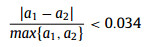
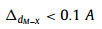
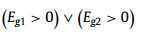
where a and Eg represent the lattice constant and bandgap of one TMD material, respectively, ΔdM−X and ΔHmix is the bond distance difference of the metal-chalcogen atoms and mixing enthalpy of the two TMD materials, respectively. Eqs. 1 and 2 request the mismatch of the lattice constants between the two TMDs to be smaller than 3%, and the difference in their metal-chalcogen bond distance better less than 0.1 Å. Eq. 3 predicts that at least one material should be semiconductor since there will be no finite bandgap exist in the alloys based on two metallic TMDs. Meanwhile, the value of the mixing enthalpy (ΔHmix) determines the miscibility of the two TMDs, and a negative ΔHmix will be favorable. Generally, alloying TMD materials between the same metal group or chalcogen is feasible due to the small lattice mismatches [34]. As shown in Fig. 1a, the 2D alloyed TMD nanosheets can be divided into three types according to the alloying sites: (1) MxM'1-xX2 type (transition metal (TM) site), (2) MX2xX'2(1-x) type (chalcogen-site), and (3) quarter-nary alloys in MxM'1-xX2yX'2(1-y) type (both TM- and chalcogen-site), where M and X denote the transition metal and chalcogen element, respectively.

|
Download:
|
| Fig. 1. (a) Selected TMD materials from the periodic table. (b) Potential applications of 2D alloyed TMD nanosheets. | |
The study of alloyed TMD crystals can date back to 1960s, such as metal (e.g., MoxW1-xS2 and MoxW1-xTe2 [47, 48]) and the chalcogen sublattices (e.g., MoS2(1-x)Se2x) [49], these materials have been proven to be thermodynamically stable at room temperature. However, the exploration of the 2D alloyed TMD nanosheets are only conducted in recent years (Fig. 1b). One of the most unique advantages of 2D alloyed TMD is the tunable bandgap [30, 38]. For example, it was reported that the direct bandgap of WS2(1-x)Se2x monolayers can be fully tuned from pure WSe2 (x = 1, Eg = 1.61 eV) to pure WS2 (x = 0, E = 1.97 eV) by adjusting the ratio of S and Se [50]. The alloying technology is also applicable for the property integration and the electronic structure adjustment of TMD materials. As is known, the carrier types in the naturally grown TMD nanosheets are different, e.g., the MoS2 and WS2 are usually presented as n-type while WSe2 and MoTe2 nanosheets are p-type semiconductors, the carrier types can be further tuned through forming alloys [38, 40, 42]. Moreover, as 2D TMD materials have diverse polymorph structures [25, 51], e.g., 1T-MoS2 and 1T'-MoS2 nanosheets are metallic and semi-metallic, respectively, alloying 2D TMDs with diverse phases opens a new avenue for phase control [44, 45, 52]. Another motivation to study the 2D TMD alloys is their better thermal stability induced by lower free energy and internal energy compared with the binary alloys (e.g., WS2 and MoS2) [36]. And from the point view of the in-plane crystal structure, the alloying of different TMD nanosheets can bring additional lattice strain in the basal plane due to the lattice mismatch [53, 54], and the incorporation of another element into the binary TMD may also increase the density of the active sites as well as the intrinsic activity. These synergistic effects could lead to the enhanced performance of alloyed TMD in electrocatalysis like hydrogen evolution reaction (HER) comparing with binary counterparts [44, 55, 56].
3. Preparation and characterization of 2D alloyed TMD nanosheetsThe widely used techniques for the synthesis of 2D alloyed TMD nanosheets can be classified into three categories: (1) Exfoliation of CVT-grown bulk crystals (e.g., mechanical exfoliation and liquid exfoliation), (2) Vapor synthesis (e.g., chemical/physical vapor deposition (C/PVD)), (3) Wet-chemical synthesis (e.g., hydrothermal synthesis and colloidal synthesis method). Generally, the alloying of TMD materials with similar structure (e.g., MoS2 and MoSe2, WS2 and WSe2) is favorable and shows precisely tunable bandgap, which is promising for (opto)electronic application. Alloying TMDs with lattice mismatch (e.g., MoTe2 and MoSe2, ReSe2 and ReS2) is not easy but will generate many interesting properties like phase transition and rich surface defects that are suitable for catalysis. Currently, the most widely studied 2D alloyed TMD nanosheets are from Groups 6 and 7 with M, M' = Mo, W, Re, V or Nb.
3.1. Phase structure/engineering of 2D alloyed TMD nanosheetsAs is known, 2D layered TMD nanosheets contain diverse phases, e.g., 1T, distorted 1T (1T' or 1T''), Td, 2H and 3R phases (the first digital indicates the layer number), which determine their fascinating electronic, optical and chemical properties [25, 57]. This feature can be ascribed to the different electronic structures of their transition metal atoms that depend on the different filling states of the d orbitals [57]. It is common to find the phase-dependent properties as well as appropriate application fields of 2D TMD materials. For example, single-layer 1H-MoS2 is semiconducting and has been recognized as one of the channel materials for next-generation FETs [22], 1TMoS2 is metallic and is promising as low-resistance contact materials for 2D FETs [58] and high-performance electrocatalyst [55], and 3R-MoS2 is a non-centrosymmetric semiconductor that has advantages for fabricating nonlinear optic devices [59]. Therefore, precisely engineering the phase structure of 2D TMD materials is a key issue in future research and applications. Currently, 2D TMD materials with thermodynamically stable phase are widely studied, such as 1H-MoS2 and 1H-WS2 that exhibit semiconducting properties. Most 1T- and 1T'-phase 2D TMD materials are (semi-)metallic, and remain difficult to be synthesized because of their metastable nature [30, 51]. However, those metastable phase-based 2D TMDs can present superior performances in catalysis, energy storage and superconductivity [57, 60, 61]. Notably, high quality 1T'-MoS2 nanosheets were prepared by Yu et al. [62], showing the best HER performance among MoS2-based electrocatalysts. More recently, high quality 1T'-WS2 nanosheets are reported by Lai et al. [63], presenting excellent superconductivity among reported TMD-based superconductors. These findings pave the way of phase-engineering of nanomaterials to further explore phase-dependent physicochemical properties and applications [51, 57].
Given such properties, alloying technology provides great convenience for further engineering the phase/phase structure of 2D TMD materials, which mainly includes two strategies: (1) 2D TMD alloys without phase transition: at the early stage, 2D TMD alloys were usually formed from Group 6 2D TMDs that focused on the composition modulation strategy, such as WS2(1-x)Se2x, MoS2(1-x)Se2x and MoxW1-xS2 that present in 2H phase as their precursors [50, 64, 65]. As expected, these 2D TMD alloys exhibited continuous tunability of electronic band structure, and the distribution of atoms is randomized due to the large phase miscibility. Notably, Group 7 based 2D TMD alloys such as 1T'-ReS2(1-x)Se2 shows unusual in-plane anisotropic optical, electrical and phonon properties, due to the lower lattice symmetry of Re-based TMDs [40]. (2) 2D TMD alloys with phase transition: in the past few years, constructing 2D alloys consisting of two materials with different phase structures has attracted great attention, such as WSe2(1-x)Te2x (2H-1Td phase), WTe2(1-x)S2x (2H-1T' phase), MoxRe1-xS (2H-1T' phase), WxRe1-xS (2H-1T' phase) and RexMo1-xSe (2H-1T'-1T'' phase), as the phase structure provides more degree of freedom for engineering their structures and properties [38, 39, 44, 45, 66]. Such phase transition enables a wide-range tunability of electronic structures, and also give rise to extraordinary physical properties. Moreover, recent breakthrough in phase engineering [62, 63, 67] of 2D TMD offers a significant opportunity to open up a whole new class of 2D TMD family, pointing out a direction of structure and property control of 2D TMD alloys for wide applications.
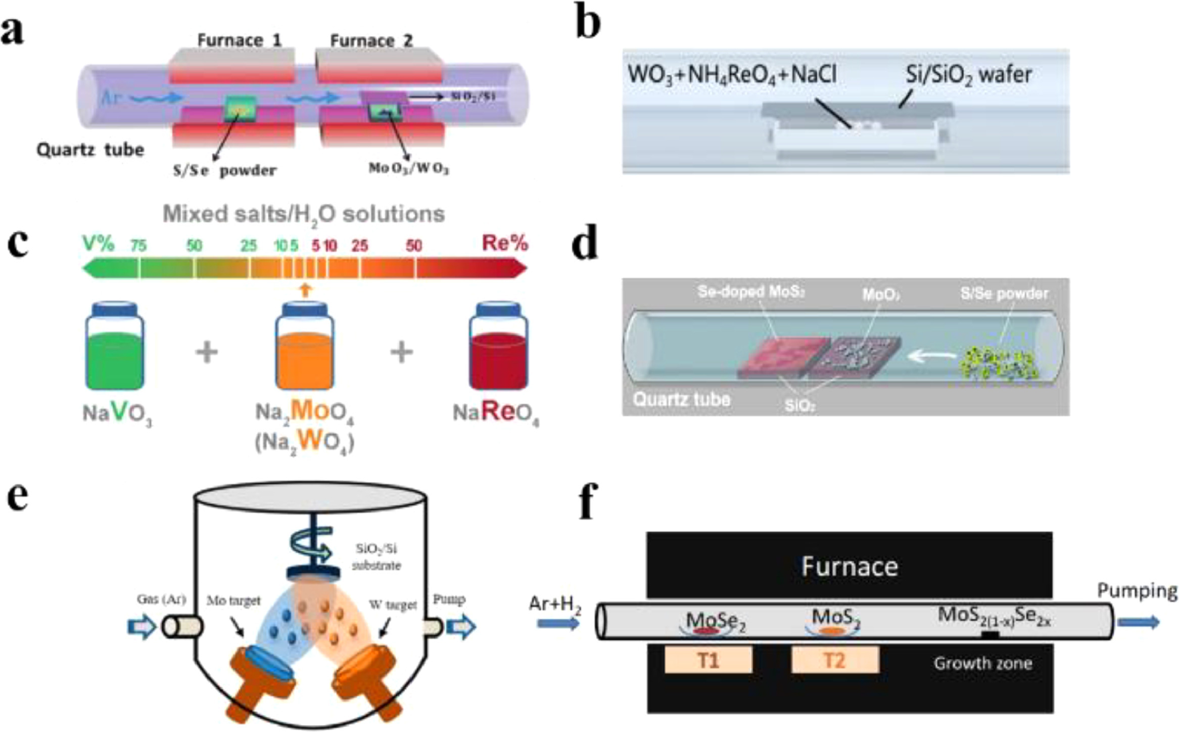
3.2. Exfoliation of CVT-grown bulk crystalsThe so-called CVT reaction addresses the crystallization of nonvolatile solids, has been widely used to produce the single crystals of various TMDs since 1960s [68]. Typical process of exfoliation of CVT-grown layered TMD crystal is shown in Fig. 2a. It starts from sealing elemental powders with transport agents (e.g., I2 and Br2) in a quartz ampoule under high vacuum, then the sealed ampoule will be annealed under a temperature gradient. During the growth, the layered TMD crystal is carried by the gas-phase transport agent in the high temperature zone (T2) and then released at the cold end (T1), which is actually a formation and decomposition of the volatile intermediates through a reversible endothermic reaction that enables the crystallization of TMD in single crystal. Generally, high temperature (~1000 ℃) and long reaction time (> 10 days) are required for the reaction. The as-prepared bulk TMD crystals can be further exfoliated into single- or few-layer 2D nanosheets. Briefly, the mechanical exfoliation of crystals can produce nanosheets with high quality but low yield and controllability, and it is usually time-consuming. On the other hand, liquid exfoliation method takes less time and shows high yield, but will generate lots defects on the surface of nanosheets.

|
Download:
|
| Fig. 2. (a) Typical process involves CVT growth bulk TMD crystals and exfoliation for nanosheets. Reproduced with permission [68]. Copyright 2012, Walter de Gruyter GmbH. (b) STEM-ADF image of Mo0.5W0.5S2, the W atoms are marked in different colors in the same image: purple, blue, light blue, green, yellow, orange and red for six-, five-, four-, three-, two-, one- and zero-coordinate sites, respectively. Reproduced with permission [69]. Copyright 2013, Nature Publishing Group. (c) An optical image and (d) layer-dependent PL spectra of Mo0.47W0.53S2. (e) Composition-dependent PL spectra of MoxW1-xS2 monolayers. Reproduced with permission [70]. Copyright 2013, American Chemical Society. (f) Composition-dependent bandgaps of WSe2(1-x)Te2x monolayers. Reproduced with permission [38]. Copyright 2017, John Wiley & Sons, Inc. (g) STEM image of ReS1.02Se0.98 and (h) crystal structure of ReS2(1-x)Se2x monolayers (side view in the top panel and top view in the bottom panel). Reproduced with permission [37]. Copyright 2017, John Wiley & Sons, Inc. | |
To date, several types of alloyed TMD nanosheets have been prepared by CVT followed by the mechanical exfoliation method. As for MxM'1-xX2 type, MoxW1-xS2 was widely studied. Dumcenco et al. [69] successfully exfoliated MoxW1-xS2 monolayers (x = 0–1) from their CVT-grown bulk crystals and quantified the degree of alloying. To begin, the powdered Mo, W, and S elements were mixed in a quartz ampoule in a double heating zone furnace system, with the charge zone maintained at 1030 ℃ (T2) and the growth zone at 980 ℃ (T1) for 20-day reaction. MoxW1-xS2 monolayers were finally obtained through the mechanical exfoliation from the as-prepared crystals using the scotch tape. Atomically resolved electron energy loss spectroscopy (EELS) and scanning transmission electron microscope (STEM) annular dark-field (ADF) method were employed to discriminate the W and Mo metal atoms. The STEM-ADF images (Fig. 2b) showed uniform 2H phase of nanosheets, and the positions occupied by W atoms were brighter than Mo atoms due to the larger annular dark-field contrast (larger Z number, Z = atomic number). Furthermore, the quantitative simulation of the STEM-ADF images revealed a random heteroatomic distribution and the alloying degree in the single-layer MoxW1-xS2, which provided a direct method for visualizing the atomic distributions at the atomic scale. The properties of MoxW1-xS2 monolayers were further revealed by Chen et al. [70], and typical optical image of the nanosheets was shown in Fig. 2c. According to PL measurements (Figs. 2d and e), MoxW1-xS2 showed a transition phenomenon from indirect to direct bandgap after thinning its bulk counterpart to monolayer, and the bandgap of its monolayers can be continuously tuned from 1.82 eV (x = 0.2) to 1.99 eV (x = 1). Meanwhile, the bandgap values did not scale linearly with the composition but show a large bowing effect which was observed in many bulk semiconducting alloys [71, 72], due to different contribution of W atoms to the highest occupied molecular orbital (HOMO) and the lowest unoccupied molecular orbital (LUMO). Further temperature-dependent PL emission and Raman scattering studies showed that characteristic peaks would redshift as the temperature increased, attributing to the an-harmonic effects and the composition disorder [73].
Similarly, MX2xX'2(1-x) type alloyed TMD nanosheets such as WS2(1-x)Se2x and MoS2(1-x)Se2x can also be prepared by above-mentioned method using stoichiometric mixture of elements as precursors, which showed uniform 2H phase structure [74, 75]. Then Yu et al. [38] firstly prepared WSe2(1-x)Te2x monolayers (x = 0–1) that showed interesting composition-dependent phase transition. Characterization results showed that the phase of WSe2(1-x)Te2x monolayers can be tuned from semiconductor 1H (x = 0–0.4) to mixed 1H and 1T' (x = 0.5–0.6), and finally the metallic 1T' (x = 0.7–1) phase. The bandgap of the WSe2(1-x)Te2x monolayers can be tuned from 1.67 eV to 1.44 eV (1H semiconductor) and drop to 0 eV (1T' metal) as revealed by the PL spectra (Fig. 2f). Meanwhile, Wen et al. [37] prepared alloyed ReS2(1-x)Se2x monolayers (x = 0–1) with unique 1T' phase structure, and the bandgap can be continuously tuned from 1.62 eV (ReS2) to 1.31 eV (ReSe2). The 1T' structure of ReS2(1-x)Se2x monolayer was confirmed according to the zigzag chains of the diamond-shaped Re4 clusters shown in the STEM image (Figs. 2g and h), and the Se atoms preferentially located inside the Re4 diamonds that was different from the random atomic distribution shown in MoxW1-xS2. Typically, polarized Raman characterization of the nanosheets showed strong anisotropic angle-dependence and Raman-mode dependence. To date, the study of TMD alloys is not limited to Groups 6 and 7 TMD alloys. Recently, Hemmat et al. [41] revealed that the alloying of TMD from Group 5 or intergroups 5 and 6 was also feasible. With the prediction of miscibility temperatures calculated by density functional theory (DFT) analysis, layered TMD alloys like MoxNb1-xS2, W1-xNbxS2, Nb1-xTaxS2, V1-xTaxS2, VS2(1-x)Se2x and TaS2(1-x)Se2x were successfully prepared by CVT method with homogeneous composition and good exfoliation capability, which boosts the further research on 2D TMD alloys.
3.2.2. Liquid exfoliation of CVT-grown bulk crystalsDifferent from the mechanical exfoliation, liquid exfoliation offers a convenient strategy to produce alloyed TMD nanosheets with high yield, but usually showed limitation in size. The commonly used methods are sonication in organic solvent and electrochemical Li-intercalation assisted exfoliation, while the latter can induce phase transition [76, 77]. Very recently, Hu et al. [33] synthesized MoxW1-xS2 crystal (x = 0.3–0.7) via the CVT method and then exfoliated it into monolayers by dispersing it in Isopropyl Alcohol (IPA) solution, which showed 1H phase with a uniform size (175 nm in average). Kiran et al. [78] exfoliated MoS2(1-x)Se2x crystal (x = 0–1) into few-layer nanosheets by sonicating it in water-ethanol mixture. The characterization results confirmed its uniform dimensions (100–300 nm) and thickness (1.4–1.9 nm). Tan et al. [77] then combined the CVT and the electrochemical Li-intercalation assisted exfoliation method to prepare MoS2(1-x)Se2x and MoxW1-xS2 monolayers, as schematically shown in Fig. 3a. The monolayers showed a lateral size ranged from few hundred nanometers to micrometers (Fig. 3b). Interestingly, the Li-intercalation process was found to induce the phase transformation, resulting in high-concentration in metallic 1T phase (around 66%) of the monolayers comparing with the 2H phase of their bulk counterparts. The Ultraviolet and visible spectrophotometry (UV–vis) absorption spectra of MoS2(1-x)Se2x evidenced the absence of the 2H phase after exfoliation process (Fig. 3c), and the HAADF-STEM analysis further confirmed its 1T phase structure as Mo atoms arranged in a triangular shape and Se atoms located in the center of the triangles. 1T phase concentration was quantified by the XPS analysis (Fig. 3d). The same group also prepared some uncommon alloyed TMD nanosheets like TixTa1-xS2OZ (x = 0.71, 0.49 and 0.30) nanosheets from CVT-prepared TixTa1-xS2 crystal in high yield by the similar method [79]. Although the nanosheets has been slightly oxidized, it still performed well as photothermal agent.

|
Download:
|
| Fig. 3. (a) Schematic illustration of the preparation of MoS2(1-x)Se2x nanosheets in metallic 1T phase. (b) AFM height image of MoS2(1-x)Se2x nanosheets (scale bars: 500 nm). (c) UV–vis spectra of exfoliated and annealed MoS2(1-x)Se2x. (d) High-resolution XPS S 2p spectrum of bulk crystal of MoS2(1-x)Se2x, and the exfoliated and annealed MoS2(1-x)Se2x nanosheets. Reproduced with permission [77]. Copyright 2016, John Wiley & Sons, Inc. | |
Since the exfoliation of CVT-prepared crystal method takes long reaction time, vapor phase growth appeared to be a promising method to prepare large scale alloyed TMD nanosheets in great flexibility and high quality, mainly including CVD and PVD. The difference of these two methods is the use of precursors. Typical schematic synthesis diagram is shown in Fig. 4a, employing the furnace as reactor and inert gas as transport agent. Precursors ① and ② represent chalcogenide and metal source, respectively, and may contain more than one component. During the reaction, precursors are usually placed at different temperature zones to achieve uniform evaporation or decomposition rates, and inert gas will continuously flow through the reactor, inducing the mixing and reaction of vapors when the heating zones reach certain temperatures. Finally, the product will be carried by inert gas and deposit on certain substrate. Different types of alloyed TMD nanosheets can be obtained by changing the precursors, and the types of precursors used are shown in Fig. 4b. Typical synthesis details are shown in Table 1 [35, 40, 42, 45, 50, 66, 80-84].

|
Download:
|
| Fig. 4. (a) Schematics of vapor phase growth of alloyed TMD nanosheets. (b) The classification of different growth methods according to the precursors. | |
|
|
Table 1 Summary of some representative vapor synthesized alloyed TMD nanosheets. |

According to Fig. 4 and Table 1, CVD can be the most flexible way to prepare alloyed TMD nanosheets with uniform and large-scale morphology (comparing with exfoliation), and it can be achieved by direct reacting sole or multiple chalcogenide sources with different metal precursors. Most of the prepared nanosheets appeared to be triangle-like morphology due to energetically preferred edge [85], and can merge into film by adjusting the synthesis parameters.
As for MxM'1-xX2 type alloyed TMD nanosheets, it is usually obtained by reacting single chalcogenide source with mixture of metal precursors. For example, Zhang et al. [35] firstly reported the one-step CVD strategy to grow the MoxW1-xS2 monolayers with controllable composition (x = 0–1) and tunable bandgap. As shown in Fig. 5a, the process took place in a dual-heating zone furnace under ordinary pressure with S and/or Se powder and MoO3 and/or WO3 powder placed at two separate heating zones. Through programmed heating, the mixture of MoO3 and WO3 powders would react with sulfur vapor to crystalize MoxW1-xS2 monolayers on a SiO2/Si substrate. The synthesized MoxW1-xS2 monolayers showed triangle-like morphology, and the Raman signals revealed the superiority of CVD over mechanical exfoliation in retaining the characteristics of the parent materials. Further research conducted by Liu et al. [36] also confirmed the better thermal stability of CVD-grown MoxW1-xS2 monolayers than the binary TMDs (e.g., WS2 and MoS2), and the phase structure of MoxW1-xS2 can be further engineered due to the great flexibility of CVD. Wang et al. [52] prepared MoxW1-xS2 monolayers (x = 0–1) with mixed phase structure (both 1H and 1T) by using a low-pressure CVD furnace system. The XPS analysis results showed that a fast-cool rate after the growth could lead to high proportions of the 1T MoxW1-xS2. Meanwhile, substrates with larger thermal expansion coefficients (TECs) (typically, the MgO) also contributed to the formation of 1T phase. A high 1T phase fraction of 60% was achieved in Mo0.4W0.6S2 at the optimized synthesis conditions. MoxRe1-xS2 monolayers have also been prepared by above-mentioned method while showed heterogeneous phase structure due to lattice mismatch. As reported by Deng et al. [39], the MoxRe1-xS2 monolayers showed two phase structures (1H or 1T') when tuning the composition, and the characteristic Raman peaks of MoxRe1-xS2 almost maintained fixed with the increase of x value, attributing to the large difference of lattice vibration modes of the two parent materials. Meanwhile, the bandgap evolution of MoxRe1-xS2 showed a strong band bowing effect with phase transition. As x changed from 0 to 0.25 (1T' phase), the bandgap decreased from 1.31 eV to 0.3 eV, while increased from 0.62 eV to 1.67 eV as x changed from 0.75 to 1 (1H phase). Since MoS2 and ReS2 also showed certain lattice mismatch [34], Wang et al. [45] used halide salt to promote the CVD synthesis of WxRe1-xS2 monolayers (Fig. 5b). The halide salt (NaCl) was employed to promote the decomposition of NH4ReO4 precursor into highly volatile Re2O7 [40]. The 2D alloys was well characterized, and the W0.2Re0.8S2 and W0.9Re0.1S2 appeared to be 1T' and 1H phase, respectively. Recently, Li et al. [42] employed mixed molten salts, e.g., Na2MoO4, Na2WO4, NaReO4 and NaVO3 for the CVD growth of alloyed 2D TMDs, as shown in Fig. 5c. The mixed molten salt showed great feasibility in controlling the composition of TMD alloys by simply changing the ratio of mixed molten salts. And thus, tunable optical and electrical properties were achieved in these 2D TMD alloys.

|
Download:
|
| Fig. 5. (a) Schematic of the tube-furnace set-up for the growth of MoxW1-xS2 monolayers. Reproduced with permission [35]. Copyright 2015, Royal Society of Chemistry. (b) Mixed metal oxides and halide salts precursors for the synthesis of WxRe1-xS2. Reproduced with permission [45]. Copyright 2020, John Wiley & Sons, Inc. (c) Mixed salt solutions with different NaReO4 and NaVO3 ratios as source precursors. Reproduced with permission [42]. Copyright 2020, John Wiley & Sons, Inc. (d) Schematic of the tube-furnace set-up for the growth of MoS2(1-x)Se2x nanosheets. Reproduced with permission [81]. Copyright 2013, American Chemical Society. (e) MoxW1-x metal film prepared by co-sputtering method. Reproduced with permission [80]. Copyright 2018, American Chemical Society. (f) Illustration of PVD synthesis of MoS2(1-x)Se2x monolayers. Reproduced with permission [89]. Copyright 2014, John Wiley & Sons, Inc. | |
As for MX2xX'2(1-x) type alloyed TMD nanosheets, it is usually obtained by reacting mixed chalcogenide sources with single metal precursor. For example, Gong et al. [81] reported the synthesis of MoS2(1-x)Se2x nanosheets with a broad range of compositions (x = 0–1) through the reaction of MoO3 with mixed S and Se vapor at 800 ℃ in an atmospheric CVD furnace (Fig. 5d). The MoS2(1-x)Se2x nanosheets can also be prepared under low pressure (P = 8 torr and T = 830 ℃) as reported by Li et al. [65], showing tunable bandgaps from 1.557 eV (x = 0) to 1.856 eV (x = 1) with little bowing effect according to the PL analysis. Interestingly, the same group [86] also achieved unique bilayer MoS2(1-x)Se2 nanosheets with continuous lateral growth composition as well as bandgaps along its structure by changing the input sequence of the precursors. Similarly, alloyed WS2(1-x)Se2x monolayers (x = 0–1) were prepared by reacting WO3 with mixed S and Se vapor as reported by Fu et al. [83]. The carrier gas flow rate has played an important role on the monolayer nucleation and growth, and the bandgaps of the samples can be continuously tuned from 1.97 eV (x = 0) to 1.61 eV (x = 1). As for TMD materials with large lattice mismatch, e.g., ReS2 and ReSe2, WS2 and WTe2, additional salts would be helpful for the alloying process. For example, Kang et al. [40] prepared ReS2(1-x)Se2x monolayers (x = 0–1) by reacting NH4ReO4/NaCl powder with S/Se vapor in an atmospheric CVD furnace. The nanosheets showed dendritic-like feature which was caused by the anisotropic growth and 1T' phase structure. The bandgaps of nanosheets showed linear dependence on the composition x in the range of 1.32 eV (ReSe2) to 1.62 eV (ReS2) according to PL measurements. While through similar synthesis method, alloyed WTe2xS2(1-x) monolayers were prepared with interesting composition-dependent bandgap and phase transition feature [66]. According to the optical microscope (OM) and TEM-ADF images, the alloyed WTe2xS2(1-x) monolayers showed triangular and elongated shape that correspond to 1H and 1T' phase, respectively, and its bandgaps could be tuned from 2 eV (for pure WS2, 1H phase) to zero bandgap (for pure WTe2, 1T' phase) as the concentration x increased, and 1H (semiconductor) to 1T' (metal) phase transition existed when x was in the range of 0.4–0.6. This phase transition was induced due to the highly deformed hexatomic rings structure of Te which would cause pairs of metal atoms to be pulled toward each other, and finally breaking the threefold symmetry of the 1H phase of WTe2xS2(1-x). Combing the results of CVT-exfoliation method, it could be found that alloying TMDs with smaller lattice mismatch leads to controllable tuning of bandgaps while the tuning range is limited. On the other hand, alloying TMDs with larger lattice mismatch leads to promising phase modulation but the synthesis process will be more challenging. Note that most of the synthesized alloyed TMD nanosheets showed limited size (Table 1), prefabricating alloyed metal membrane may be a promising strategy to produce alloyed TMD nanosheets with large scale (Fig. 5e) [80, 87]. For example, Liu et al. [87] firstly prepared the large scale (2-inch) MoxW1-xS2 (x = 0–1) atomic layers by sulfurizing the as-prepared MoxW1-x thin films, which was pre-deposited on 2-inch c-plane sapphire substrates by co-sputtering Mo and W targets. The XPS analysis confirmed the feasibility of the method as the W content in MoxW1-xS2 increased linearly with the increase in the powder ratio of W/(Mo + W), and peak-fittings of the Raman spectra across the 2-inch wafer showed low variation (5%), revealing the uniformity of the synthesized nanosheets. Similar strategy was also reported by Park et al. [80], and an additional laser thinning process was employed to thinner the thickness of MoxW1-xS2 nanosheets.
The CVD method is also feasible to synthesize MxM'1-xX2yX'2(1-y) type TMD alloys. Susarla et al. [84] prepared alloyed MoxW1-xS2ySe'2(1-y) nanosheets by reacting Se/S vapor with mixture of ammonium molybddate tetrahydrate (AT) and ammonium meta tungstate (AMT), which showed a wide range of bandgap tunability from 1.60 eV to 2.03 eV. Very recently, a modified sequential two-stage CVD process was employed by Zhang et al. [88] to prepare bilayer MoxW1-xS2ySe'2(1-y) nanosheets with large size (~200 µm) and high controllability. Typically, reverse hydrogen flow was introduced during the growth stage, both to reduce the undesired nucleation centers of the first layer as well as to promote the homogeneous growth of the second monolayer.
3.3.2. Physical vapor depositionFor some TMD materials with high sublimation rate, the alloying process can be simplified by direct heating the two materials. For example, Xie's Group [82, 89] prepared the PVD-grown MoS2(1-x)Se2x (x = 0–1) monolayers by employing double heating zone furnace using MoSe2 and MoS2 as precursors (Fig. 5f). The characterization results indicated that the increase in evaporation temperature of MoSe2 lead to a tunable growth of MoS2(1-x)Se2x with larger size but limited Se content (x = 0–0.40), this problem arose from the decomposition of MoSe2 to Mo3Se4 at high temperatures and was solved by adding extra Se vapor during PVD. The as-prepared alloyed monolayers also showed a tunable bandgap (from 1.86 eV (x = 0) to 1.55 eV (x = 1)). WS2(1-x)Se2x (x = 0–1) monolayers can also be prepared by co-evaporation method. As revealed by Duan et al. [50], the PL and Raman studies of WS2(1-x)Se2x (x = 0–1) monolayers showed a systematic shift of PL peak position and the Raman resonance frequencies, indicating a successful chemical and structural modulation and tunable bandgaps from pure WSe2 to pure WS2.
Briefly, the vapor phase synthesis is convenient to obtain different types of alloyed TMD nanosheets with tunable bandgap comparing with CVT method, but many challenges remain. The adjustment range of bandgap and size of the 2D alloys are still limited, and how to precisely control its phase structure is another challenge. The uniformity and reproducibility of synthetic 2D alloys need to be carefully considered before we can generate a scalable synthesis method for future lab-to-industry application.
3.4. Wet-chemical synthesisDifferent from the vapor synthesis method that required high temperature, hydrothermal method is carried under lower temperature, presenting an attractive alternative with the potential for higher-yield, substrate-free synthesis of larger-surface-area 2D TMD alloys as well as vacancy engineering [90]. In terms of the MxM'1-xX2 type, Sun et al. [91] reported a simple colloidal synthesis method to prepare MoxW1-xSe2 nanosheets with tunable optical properties by injecting metal reagents (mixture of MoCl5, WCl6 and oleic acid) into as-prepared chalcogen-contained precursors (hot mixture of 300 ℃) of diphenyl diselenide, oleylamine and hexamethyldisilazane (HMDS)). As shown in Figs. 6a and b, TEM and energy dispersive spectrometer (EDS)-mapping images confirmed the buckled nanoflower structure of MoxW1-xSe2 nanosheets with uniform elemental distribution, and the ADF-STEM images of the sample presented the Mo vs. W site occupancies as well as three chalcogen configurations (namely diselenium (Se2), monoselenium vacancy (VSe), and diselenium vacancy (VSe2)). The bandgaps of the samples showed a complete tunability between the two ends TMDs (1.51–1.61 eV). Phase engineering of 2D alloys can also be achieved by wet-chemical method. For example, Yang et al. [92] prepared MoxW1-xS2 nanoflowers (x = 0.04–0.13) with 1T/2H phase (Fig. 6c) by heating mixture of (NH4)10W12O41·xH2O, (NH4)6Mo7O24·4H2O, and thiourea under certain temperature (200 ℃, 220℃ or 240 ℃). Furthermore, Kwak et al. [44] prepared MoxRe1-xSe2 nanosheets (x = 0–1) with phase evolution. As revealed by the schematic synthesis diagram (Fig. 6d), powder precursors of Na2MoO4·2H2O and NaReO4 were dissolved in the deionized water with 4-mmol NaBH4 as the reductant, and MoxRe1-xSe2 nanosheets were obtained under the temperature of 240 ℃. Distinct phase transition of MoxRe1-xSe2 was observed, i.e., the major phase is 1T'' (triclinic, distorted 1T) for x = 0–0.4, 1T' (monoclinic, distorted 1T) for x = 0.6, and 2H for x = 0.8–1.

|
Download:
|
| Fig. 6. (a) TEM image and (b) scanning transmission electron microscopy-energy dispersive X-ray spectroscopy (STEM-EDS) element maps (100-nm scale bars) of Mo0.35W0.65Se2 nanostructures. Reproduced with permission [91]. Copyright 2017, American Chemical Society. (c) Cs-corrected STEM image of the MoxW1-xS2 nanosheets, the red and blue squares represent the 2H and 1T structures, respectively. Reproduced with permission [92]. Copyright 2017, The Royal Society of Chemistry. (d) Schematic diagram for the synthesis of Re1-xMoxSe2 nanosheets (calculated ball-stick models, where green, purple, and golden balls represent Re, Mo and Se atoms, respectively). Reproduced with permission [44]. Copyright 2020, American Chemical Society. (e, f) Magnified high-resolution STEM images for MoSSe and (g) Intensity profile of the blue area indicated in image (f). Reproduced with permission [94]. Copyright 2019, American Chemical Society. | |
As for MX2xX'2(1-x) type, Xu et al. [93] illustrated a novel liquid interface-mediated strategy to prepare MoSSe monolayers by direct heating the (NH4)6Mo7O24·4H2O, and S/Se powder dissolved in the oleylamine/water solution in teflon-lined autoclave at 220 ℃, then MoSSe nanosheets were flexibly formed at the oil/water interface. The X-ray absorption fine structure spectroscopy (XAFS) measurements revealed the disordered structure of MoSSe with shorter Mo-S and longer Mo-Se bond comparing with the pure MoS2 and MoSe2 monolayers, which helped to further tailor the electronic structure of Mo atoms. More recently, inspired by the vacancy engineering, He et al. [94] reported a simple alloying reaction to prepare MoS2(1-x)Se2x nanosheets (x = 0–1) with tunable anion vacancies concentration. The mixture of MoSe2 (prepared by hydrothermal method) and S powder were prepared first, then vacuum sealed and calcinated at 700 ℃ to obtain MoS2(1-x)Se2x nanosheets (12 nm in thickness). Defect and vacancy features of samples were revealed by STEM analysis (Figs. 6e-g), and the electron paramagnetic resonance (EPR) analysis showed that the vacancy concentration increased firstly with the increase of x value and then reduced, reaching the highest value at x = 0.25.
3.5. Other methodsThe alloyed TMD nanosheets can also be prepared via other advanced methods with great potentiality. For example, Yao et al. [95] reported the growth of high-quality Mo0.5W0.5S2 nanosheets with centimeter-scale and thickness of 20 nm via pulsed laser deposition (PLD). The nanosheets was highly c-axis-oriented since only one pronounced peak indexed as (0 0 2) was found in the XRD pattern. Zhang et al. [96] employed the molecular beam epitaxy (MBE) method which was widely used in the semiconductor heterostructure to fabricate VxMo1-xSe2 monolayers with tunable composition (x = 0–1). The synthesis of these alloyed nanosheets was carried out under ultrahigh vacuum, and Se was evaporated from a Knudsen cell while V and Mo were co-evaporated from two electron-beam evaporators with their evaporation rates controlled by the flux current. The value of x = 0.44 acted as a critical point while below which the phase separation occurred and above which a homogeneous metallic 1H phase was favored. Most of the methods focused on TMD precursors with thermodynamically stable phase, while notably, Lai et al. [63] successfully obtained high quality and large scale metastable 1T' MoS2(1-x)Se2x and WS2(1-x)Se2x nanosheets by a multi-step thermal reaction followed by mechanical exfoliation. As an example of MoS2(1-x)Se2x, mixtures of K2MoO4 with S and Se powder were firstly grounded and sealed within a quartz ampoule under internal pressure of about 10−6–10−5 Torr. After heated at 500 ℃ for around 100 h, the as-prepared intermediate would be treated under the flow of Ar/H2 mixed gas. Finally, the 1T'-MoS2(1-x)Se2x crystals were obtained by purification and drying process, and then exfoliated into single or multi-layer nanosheets.
4. Applications of 2D alloyed TMD nanosheets 4.1. Electronics2D TMD nanosheets are widely considered as attractive semiconducting channel materials, due to their atomically thin thickness, high carrier mobility and current on/off ratio [22, 97]. Meanwhile, 2D TMD alloys have unique properties such as tunable bandgap/band position, phase structure and electrical conductivity compared with their binary counterparts, thus making them promising candidates for not only the channel materials but also the electrode materials of 2D FETs [42, 98, 99].
FETs that employ 2D TMD alloys as channel materials were studied at an early stage, more efforts are needed to seek ideal alloys with enhanced FET performance. Compared with the intrinsic 2D TMD nanosheets, most of the reported 2D TMD alloys demonstrated similar or poor FET performance. As for the MxM'1-xX2 type, Liu et al. [36] reported WxMo1-xS2 monolayer-based FETs on SiO2/Si substrates for the first time. The WMoS2-FET demonstrated typical n-type transport behavior and similar high current on/off ratio as the intrinsic MoS2 and WS2 monolayers (Fig. 7a). The electron mobility of WMoS2-FET was ~54 cm2 V−1 s−1 at 20 K and ~30 cm2 V−1 s−1 at 300 K (Fig. 7b) which is somehow in between the MoS2 and WS2 monolayers. As for MX2xX'2(1-x) type, Duan et al. [50] demonstrated the interesting composition-dependent electronic properties of WS2(1-x)Se2x monolayer-based FETs. According to the evolution of electrical properties of FETs (Isd1/2–Vg plot, Fig. 7c), highly p-type behavior was observed in Se-rich alloy (brown curve), while gradually shifted to highly n-type in S-rich alloys (black curve). As shown in Fig. 7d, the extracted average threshold voltage (Vt) of the FETs decreased (more negative) with increasing S ratio, suggesting the reduced electron density and increased hole density. Meanwhile, the achieved mobility value (Fig. 7e) decreased firstly from the Se-rich end (68.2 cm2 V−1 s−1 for holes), reaching a lowest value at x ≈ 0.5 and then increased to 11.8 cm2 V−1 s−1 (electrons) at S-rich end. The low electron mobility was ascribed to the higher contact resistance due to the lower doping concentration, and also the ionized impurity scattering and alloy scattering commonly seen in Groups 3–5 alloy semiconductors [100, 101]. The WS2(1-x)Se2x-based FETs also presented thickness-dependent transport mechanism as revealed by Karande et al. [74], showing n-type and ambipolarity behavior in thinner and thicker samples, respectively. This FET device also showed promising performance, exhibiting a maximum electron mobility of ~50 cm2 V−1 s−1 along with an on/off ratio > 106.

|
Download:
|
| Fig. 7. (a) ID–VG transfer characteristic (VD = 0.5 V) at 300 K of the fabricated FETs, the inset shows the optical image of monolayer WxMo1-xS2 FETs. (b) Field effect mobility µ as a function of the measurement temperature. Reproduced with permission [36]. Copyright 2017, John Wiley & Sons, Inc. (c) Transfer characteristics (Id1/2–Vg plot) of WS2(1-x)Se2x nanosheet transistors with different S atomic ratio from nearly pure WSe2 (brown curve) to nearly pure WS2 (black curve). (d) Alloy nanosheet transistor threshold voltage (Vt) vs. S atomic ratio, with the blue dots highlighting the p-type behavior in WSe2-rich alloys and red dots highlighting the n-type behavior in WS2-rich alloys. (e) Field effect mobility vs. S atomic ratio relationship in alloyed WS2(1-x)Se2x nanosheets, with the blue dots representing the hole mobility in WSe2-rich alloys and red dots representing the electron mobility in WS2-rich alloys. Reproduced with permission [50]. Copyright 2016, American Chemical Society. (f) Transfer curves (Ids–Vg) of MoxRe1-xS2 alloy FETs with different Mo compositions. Reproduced with permission [39]. Copyright 2020, John Wiley & Sons, Inc. (g) Typical I-V curves of intrinsic MoS2 and MoxNb1-xS2 monolayers. (h) Typical Nb composition dependent transport curves of MoxNb1-xS2 monolayers. Reproduced with permission [99]. Copyright 2020, American Chemical Society. (i) Typical V composition dependent transport curves of WxV1-xS2 and WxV1-xSe2 monolayers. (j) Typical transport curves of WSe2-FETs with three different contacts: Au, Pd and WxV1-xSe2. Reproduced with permission [42]. Copyright 2021, John Wiley & Sons, Inc. | |
In addition, the carrier type and density of Group 6 2D TMD nanosheets can be well tuned when alloying with neighboring Re (electron donor), or V and Nb (electron acceptor) in periodic table [42, 99]. And thus, their electrical properties can be tuned in a large range, from intrinsic semiconductors to heavily alloyed metals. These TMD alloys showed great potential in overcoming the high contact resistance between metal electrodes and 2D TMD nanosheets. For the MxRe1-xX2 type, Deng et al. [39] fabricated the back-gated FETs based on MoxRe1-xS2 monolayers that showed conduction transition behavior from n-type to bipolar and p-type in 1T' phase, and novel "bipolar-like" conduction behavior contributed by the electron current in 2H phase alloys (Fig. 7f). Besides the MxRe1-xX2, the MxNb1-xX2 and the MxV1-xX2 show the most impressive composition dependent electrical conductivity. Chuang et al. [98] demonstrated a unique Nb0.005W0.995Se2/WSe2 electrode contacts for WSe2 based-FETs. The 2D/2D contacts exhibited low contact resistances of ~0.3 kΩ·µm and high on/off ratios up to > 109. Gao et al. [99] reported the growth of wafer-scale MoxNb1-xS2 monolayers with tunable Nb composition via metal–organic chemical vapor deposition (MOCVD) growth. The as-grown MoxNb1−xS2 showed a dramatical increment of electrical conductivity up to 107 when compare with the intrinsic MoS2 monolayers (Figs. 7g and h). Similarly, Li et al. [42] also observed the dramatic enhancement of electrical conductivity up to 108 in WxV1-xS2 and WxV1-xSe2 (Fig. 7i). These metallic TMD alloys were ideal van der Waals contacts for 2D FETs. They can eliminate the high contact resistance caused by Fermi level pinning effect at the interface of metal electrode and TMD nanosheets. As shown in Fig. 7j, when the metallic WxV1-xSe2 monolayers were used as contacts, the on-state current and current on/off ratio of WSe2-FETs increased 1~3 orders of magnitude when compare with the widely used Pd and Au electrodes. Using metallic 2D TMD alloys provide a practical strategy to engineer the contacts for high-performance 2D FETs.
Alternatively, tunable carrier type and density can also be achieved in MX2xX'2(1-x) alloys. Cui et al. [102] synthesized 1T' ReS2xSe2(1-x) monolayer with an interesting tunable conductivity from n-type (x = 0.6–1.0) to bipolar (x = 0.3–0.6) and p-type (x = 0–0.3). Moreover, the electrical transport properties of the 2D alloys-based FETs showed obvious lattice direction dependence, where both electron and hole mobility of the FET channel along the b-axis was larger than that perpendicular to the b-axis. Yu et al. [38] employed the bilayer WSe2(1-x)Te2x as the channel materials for back-gated FETs, which showed interesting phase dependent electrical properties. The calculated mobility and on/off ratio of 2H WSe2(1-x)Te2x (p-type) at x = 0 and 0.3 were 10 cm2 V−1 s−1 with 106, and 46 cm2 V−1 s−1 with 106, respectively, whereas no drain current dependency was found in WSe2(1-x)Te2x with x > 0.7, suggesting its metallic properties. This study provides a strategy to create a WSe2(1-x)Te2x homojunction which can work as channel and electrode materials of 2D FETs simultaneously.
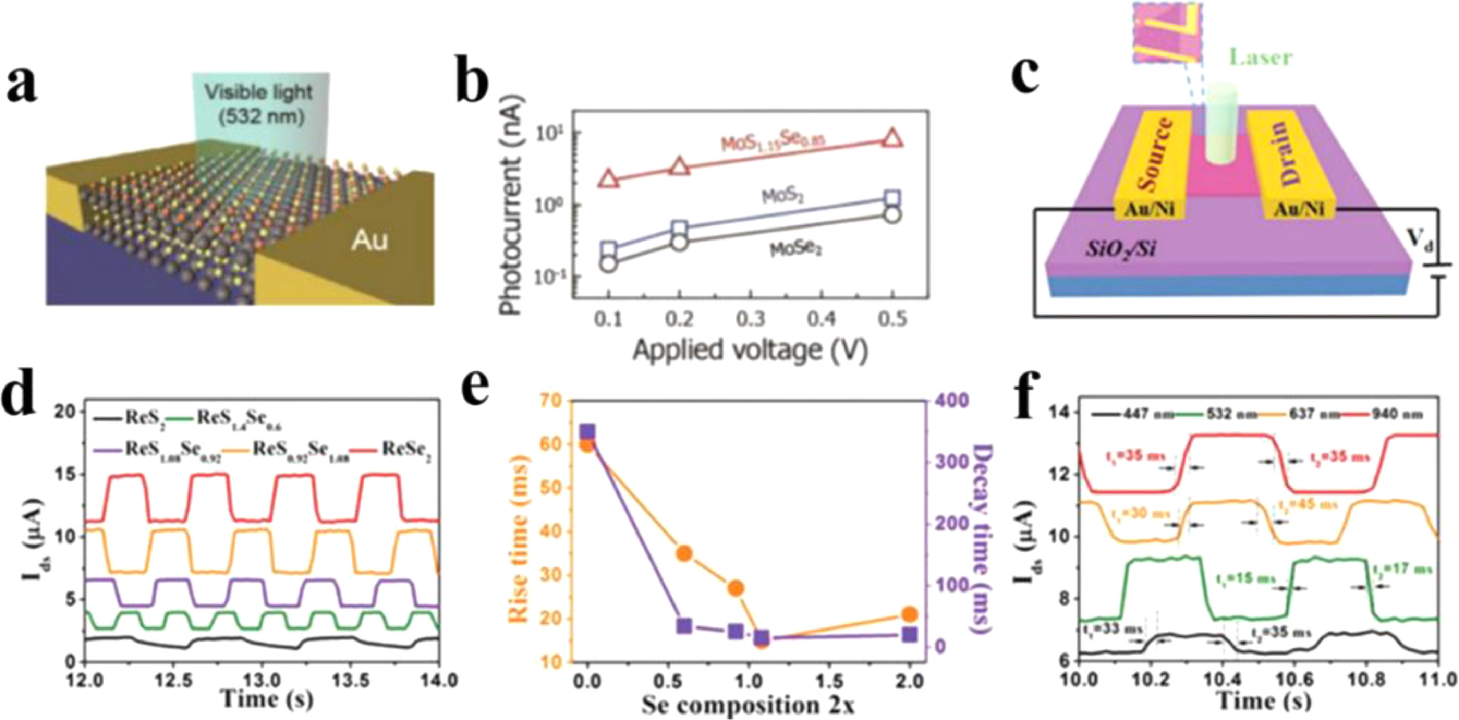
4.2. PhotodetectorsBesides the applications in FET devices, 2D alloyed TMD nanosheets have also exhibited great potential in fabricating high-performance photodetectors, due to its tunable bandgap in tuning the peak responsivity position and photo-response edge [103-106]. Yao et al. [95] demonstrated the fabrication of photodetector based on PLD-prepared alloyed Mo0.5W0.5S2 nanosheets with better responsibility than PLD-prepared WS2. The resulting photodetector possessed stable photoresponse from 370 nm to 1064 nm with a responsivity of 5.8 A/W and a response time shorter than 150 ms. The favorable results laid in the suppression of the depth and number of deep-level defect states (DLDSs) due to the alloy engineering to improve the thermodynamic stability. More recently, Wang et al. [45] employed WxRe1-xS2 monolayers for photodetector and found that the device based on 1H-W0.9Re0.1S2 alloy displayed a high photoresponsivity of 17 µA/W in air than WS2 (0.2 µA/W), attributing to the existence of trap states and the absorption of light. However, it also showed a worse response time. Klee et al. [107] studied the photo-response of the CVD-grown MoS2(1-x)Se2x monolayers using the spatially resolved photocurrent measurement (laser powers = 190–1320 µW at λ = 633 nm). Interestingly, the author found an unusual photoresponsivity transition in the MoS2(1-x)Se2x-based devices from notably nonlinear to nearly linear current–voltage when increasing the Se content. It was worth noting that Lim et al. [108] prepared the large-scale MoS2(1-x)Se2x multilayers on a 4-inch quartz wafer through thermal decomposition method for photoelectrical application, and 20 devices were fabricated with identical geometry on a single chip to evaluate the device-to-device variations in terms of the photocurrents (Fig. 8a). As a typical example, Fig. 8b showed that the photocurrent of the MoS1.15Se0.85based FET was higher than those of the MoS2 and MoSe2based devices, which can be explained by two synergetic effects: (1) The decrease in density of localized DLDSs and (2) Deep-to-shallow level transition induced by the alloy formation. The spatial homogeneity test further revealed the excellent reproducibility of the device. Moreover, the photoresponsivity of the MoS1.15Se0.85-based device reached 2.06 A/W at 10 V, which was greater than those of the commercial photodetectors based on Si and GaAs. Kang et al. [40] prepared the CVD-grown ReS2(1-x)Se2x monolayer in high crystal quality for photodetector, and the schematic image of the device was shown in Fig. 8c. The study of the temporal time-dependent photo-response of the ReS2(1-x)Se2x-based devices were shown in Figs. 8d and e, revealing that the incorporation of Se within Re-based TMDs could reduce the response time, which was attributed to the modulation of the defect-induced trap states. Typically, the ReS0.92Se1.08-based photodetector exhibited a fast response time less than 15 ms. The ReS0.92Se1.08-based device also showed wide photo-response from visible (447, 532 and 637 nm) to near-infrared (940 nm) light (Fig. 8f), and the photocurrent rose gradually with the increase of the laser wavelength except for a singular point at 532 nm, which showed the highest photocurrent.

|
Download:
|
| Fig. 8. (a) Schematic illustration of MoS1.15Se0.85-based visible light photodetector. (b) Plots of the photocurrent of MoS2, MoSe2 and MoS1.15Se0.85 as a function of bias voltage. Reproduced with permission [108]. Copyright 2019, John Wiley & Sons, Inc. (c) Schematic diagram of a back-gated ReS2(1-x)Se2x photodetector. (d) The time-dependent photo-response of the ReS2(1-x)Se2x photodetector with different compositions of Se. (e) The plots of the rise and decay time measured at a bias of 1 V as a function of Se composition. (f) The rise and decay times of the ReS2(1-x)Se2x photodetector under different light wavelength. Reproduced with permission[40]. Copyright 2019, John Wiley & Sons, Inc. | |
The hydrogen evolution reaction (HER), in which the molecular H2 is formed through the reduction of the absorbed protons on the electrode, is considered as an effective route to achieve high-performance water splitting [77]. Currently, 2D TMD nanosheets have been proven to be promising catalysts, and alloying technology offers the possibility to further engineer H2 affinity as well as defect structure in 2D TMD alloys, therefore resulting in enhanced HER performance than the binary TMD nanosheets [44, 55, 56].
For the MxM'1-xX2 type, Nguyen et al. [109] prepared the MoWS2 nanosheets coating on carbon nanotube yarn (CNTY) and carbon cloth (CC) substrates by low-temperature thermolysis method for HER. The MoWS2/CC showed small Tafel slope and overpotential of 41.8 mV/dec and 145 mV (η10, means that the overpotential values were obtained at a current density of 10 mA/cm2), respectively, which was the closest to that of Pt/C (Tafel slope of 31.4 mV/dec). MoxRe1-xSe2 nanosheets (x = 0–1) were synthesized by hydrothermal reaction for HER by Kwak et al. [44]. As shown in Figs. 9a and b, the linear sweep voltammetry (LSV) analysis and Tafel plots confirmed the better performance of MoxRe1-xSe2 compared with its binary counterparts, with an overpotential of 77 mV (η10) and a Tafel slope of 42 mV/dec. Then the calculation of Gibbs free energy (Fig. 9c) along the reaction path indicated that the high activity of Mo0.1Re0.9Se2 originated from the formation of the Mo-H provided the existence of the adjacent Se vacancies. For the alloyed TMDs in MX2xX'2(1-x) type, similarly, Kiran et al. [78] found that the exfoliated MoS2(1-x)Se2x nanosheets possessed higher HER activity than pristine MoS2 and MoSe2 nanosheets. A high exchange current density of 320 µA/cm2 for a constant loading of 180 µg/cm2 and a Tafel slope of 56 mV/dec were achieved by the prepared MoSSe in N2-saturated 0.5 mol/L H2SO4 electrolyte. The MoSSe also showed good stability without detectable difference between the initial voltammogram and the one after 1000 cycles. In addition, high-temperature solution prepared few-layer MoS2(1-x)Se2x was also applied for HER by Gong et al. [56]. The MoS2(1-x)Se2x nanoflakes have high activity and durability for HER electrocatalysis with small overpotentials in the range of 80–100 mV and the negligible activity loss up to 10, 000 potential cycles. Meanwhile, the alloyed MoSSe obtained the lowest overpotential of ~160 mV (η10) and Tafel slope of ~48 mV/dec, with the highest TOF (turnover frequency, s−1) of 150 mV. The enhanced activity was attributed to the modulation of the d-band electronic structure to tune the hydrogen adsorption free energy and the consequent electrocatalytic activity. Particularly, Tan et al. [55] prepared MoS2, WS2, MoSe2, Mo0.5W0.5S2 and MoSSe nanodots by Li-assisted exfoliation for HER reaction. Impressively, the obtained MoSSe achieved a low overpotential of 140 mV (η10), Tafel slope of 40 mV/dec, faster Faradic process and excellent long-term durability (Figs. 9d and e). Combing the DFT calculation, the excellent catalytic activity of MoSSe nanodots was attributed to the high-density active edge sites, high-percentage metallic 1T phase (60%), alloying effect and basal-plane Se-vacancy (Fig. 9f). Wang et al. [110] then reported the CVD-grown dendritic WS2(1-x)Se2x monolayers for enhanced HER. The dendritic WS2(1-x)Se2x nanosheets revealed a much lower overpotential and Tafel plot than that of WS2 nanosheets, suggesting that the dendritic shape of flakes provided more active edge sites than triangular flakes, thereby resulting in an improved HER performance.

|
Download:
|
| Fig. 9. (a) LSV curves (scan rate: 2 mV/s) for MoxRe1-xSe2 and commercial Pt/C as catalysts toward HER in H2-saturated 0.5 mol/L H2SO4 (pH 0). (b) Tafel plots derived from the LSV curves at low potentials which correspond to the activation-controlled region, using the Tafel equation of η = blog(J/J0), where η is the overpotential, b is the Tafel slope (mV/dec), J is the measured current density, and J0 is the exchange current density. (c) Gibbs free energy (ΔGH*) diagrams for the HER at x = 0% (ReSe2), 12.5%, 50% and 100% (MoSe2) and those with CVSe = 6.25% at x = 0% and 12.5%. Reproduced with permission [44]. Copyright 2020, American Chemical Society. (d) Electrochemical impedance spectroscopy Nyquist plots of MoSSe, MoS2, Mo0.5W0.5S2, WS2 and MoSe2 nanodots at the working potential of −0.198 V (vs. RHE). Inset: The corresponding fitting equivalent circuit, where Rs represents the uncompensated resistance, Rp represents the charge transfer resistance, CPE is the value of the argument of the constant phase element, and n is the value of the exponent of the constant phase element. (e) Stability measurement of MoSSe nanodots for HER. (f) Atomic models for hydrogen atoms adsorbing at the active sites of basal planes of 1T-phase MoS2 nanodots, 1T-phase MoSSe nanodots, 1T-phase nanodot in presence of S vacancy, and 1T-phase MoSSe nanodot in presence of Se vacancy. VS and VSe represent the S and Se vacancies, respectively. Reproduced with permission [55]. Copyright 2018, John Wiley & Sons, Inc. | |
In addition to the as mentioned applications, some other promising ones involving 2D alloyed TMD nanosheets have also been reported in recent years. For example, Tan et al. [77] revealed that single-layer MoS2(1-x)Se2x with high 1T phase (66%) were efficient electrocatalyst for the tri-iodide reduction on the counter electrode in a dye-sensitized solar cell (DSSC). As shown in Fig. 10a, MoS2(1-x)Se2x nanosheets were coated on a fluorine-doped tin oxide (FTO) substrate by simple drop-coating method to form the counter electrode, and Fig. 10b further revealed that the MoS2(1-x)Se2x nanosheets/FTO counter electrode presented comparable photovoltaic performance (PCE) comparing with Pt/FTO. The MoS2(1-x)Se2x nanosheets showed a PCE of 6.5% that was higher than that of the 2H-MoS2(1-x)Se2x (5.4%) and MoS2 (6.0%). They also found that TixTa1-xS2Oz were highly effective for photothermal therapy [79]. Typically, the Ti0.71Ta0.29S2Oz nanosheets exhibited strong absorption intensity in the near-infrared region (large extinction coefficient of 54.1 L g−1 cm−1 at 808 nm). After modified with lipoic acid-conjugated polyethylene glycol (LA-PEG) to increase the physiological stability, the modified Ti0.71Ta0.29S2Oz nanosheets showed a high photothermal conversion efficiency of 39.2%, with the solution temperature increasing by 34.4 ℃ after 10 min irradiation using an 808 nm laser at a power density of 1.0 W/cm2 (Fig. 10c). Notably, low viabilities of HeLa cells incubated with 20 and 50 ppm LA-PEG-modified Ti0.71Ta0.29S2Oz nanosheets were obtained by irradiating the cancer cells with the 808 nm laser, further revealing its potential as photothermal agent (Fig. 10d). Meanwhile, 2D alloyed TMD nanosheets can also be attractive candidates for energy storage and conversion, due to defects or phase engineering in enhancing the activities. Cai et al. [111] reported defect-rich few-layer MoS2(1-x)Se2x nanocomposites for Li-ion batteries. A co-etching method was employed to increase the active edges sites, and the MoS1.5Se0.5 nanosheets showed best performance, e.g., special capacity of up to 500 mAh/g at the large current density of 5 C after 350 cycles, and the coulombic efficiency was close to 100%. Similarly, alloyed MoS2(1-x)Se2x nanosheets with anion vacancies were reported by He et al. [94] for potassium ion battery. The anion vacancies in MoS2(1-x)Se2x nanosheets could enhance the electronic conductivity by inducing more active sites and alleviating structural variation in the alloys. The most optimized vacancy-rich MoSSe alloy showed high reversible capacities of 517.4 and 362.4 mAh/g at 100 and 1000 mA/g, respectively. Moreover, a reversible capacity of 220.5 mAh/g could be maintained at 2000 mA/g after 1000 cycles.

|
Download:
|
| Fig. 10. (a, b) DSSCs based on MoS2(1-x)Se2x nanosheets: (a) Schematic illustration of a typical assembled DSSC with N719 dye-sensitized TiO2 photoanode and FTO-exfoliated-MoS2(1-x)Se2x CEs. (b) J–V curves of DSSCs with FTO-exfoliated- MoS2(1-x)Se2x, FTO-Annealed-MoS2(1-x)Se2x, and FTO-Pt used as CEs measured under simulated sunlight 100 mW/cm2 (AM 1.5). Reproduced with permission [77]. Copyright 2016, John Wiley & Sons, Inc. (c) Photothermal heating curves of pure water and solutions of LA-PEG modified Ti0.71Ta0.29S2Oz nanosheets at concentrations of 5, 20 and 50 ppm. Irradiation wavelength is 808 nm. (d) Relative viabilities of Sk-mel-28 and HeLa cells incubated in LA-PEG-modified Ti0.71Ta0.29S2Oz nanosheets at different concentrations (0, 20 and 50 ppm) under laser irradiation (λ = 808 nm). Reproduced with permission [79]. Copyright 2017, John Wiley & Sons, Inc. | |
In this review, we have summarized the latest research progress on the preparation, characterization and applications of 2D alloyed TMD nanosheets. Different synthesis methods have their own features. For example, the exfoliation of CVT-grown crystals is a convenient way to study the thickness-dependent properties of 2D alloyed TMD nanosheets, and the CVD method appears to be the most promising and flexible way to synthesize alloyed TMD nanosheets with high quality and large area, which is suitable for electronic and optoelectronic applications. Wet-chemical synthesis, on the other hand, favors the atomic engineering (e.g., interface and defect engineering) of alloyed TMD nanosheets, is usually employed for catalytic application. Various characterization techniques like OM, AFM, HAADF-STEM, PL analysis, Raman, and XPS were employed to reveal the sizes, thicknesses, atomic arrangements, bandgaps, phase structure, and compositions of 2D alloyed TMD nanosheets. Owing to their advantages compared with 2D TMD nanosheets, 2D alloyed TMD nanosheets exhibited enhanced performance in many applications, such as electronics, optoelectronics, and catalysis.
Given the unique properties of 2D alloyed TMD nanosheets, there are still lots of challenges but also opportunities remain. Firstly, the controllable synthesis of 2D alloys with high quality, stability, and uniform large area still remains a key challenge. As is known, both CVD and CVT requires high temperature that may affect the surface properties of the prepared 2D alloys, and for the wet-chemical synthesis, it is difficult to precisely control the thickness and size of the 2D alloys. Therefore, exploring novel approaches or improving the current technique is urgently required to control and engineer the structure of the 2D alloyed TMD nanosheets, especially with large area (e.g., in centimeter level). Secondly, most of the recent works still concentrate on Groups 6 and 7 TMDs, while new 2D alloyed TMD nanosheets like W1-xNbxS2, Nb1-xTaxS2 and V1-xTaxS2 can also be prepared by the method introduced before. Therefore, to explore novel 2D alloyed TMD nanosheets (e.g., Groups 4 and 5 TMDs) is also a promising direction. Moreover, with the development of phase-engineering of nanomaterials, alloying 2D TMDs with diverse phases is another promising and challenging topic. Thirdly, the application of 2D alloyed TMD nanosheets is still limited and its potential has not been fully explored. For example, although the 2D alloyed TMD nanosheets showed interesting tunable electronic and optoelectronic properties which are desired in making FETs or photodetectors, the performance is less than satisfactory, key factors such as high dark current and low photo-detectivity issues need to be addressed. Meanwhile, the 2D alloyed TMD nanosheets were mostly employed for HER in catalysis, while other applications like electrocatalytic CO2 reduction, batteries, and environmental treatment are rarely explored. Therefore, the exploration of novel applications based on 2D alloyed TMD nanosheets is also a key issue.
Declaration of competing interestThe authors report no declarations of interest.
AcknowledgmentsC.Tan thanks the funding support from the Start-Up Grant (No. 9610495) from City University of Hong Kong and National Natural Science Foundation of China (No. 22005259). S.Li acknowledges the funding support from JSPS-KAKENHI (Nos. 19K15399, 21K04839).
| [1] |
C. Tan, X. Cao, X.J. Wu, et al., Chem. Rev. 117 (2017) 6225-6331. DOI:10.1021/acs.chemrev.6b00558 |
| [2] |
C. Tan, H. Zhang, Chem. Soc. Rev. 44 (2015) 2713-2731. DOI:10.1039/C4CS00182F |
| [3] |
Y. Ge, Z. Shi, C. Tan, et al., Chem 6 (2020) 1237-1253. DOI:10.1016/j.chempr.2020.04.004 |
| [4] |
A. Chaturvedi, B. Chen, K. Zhang, et al., SmartMat 1 (2020) e1011. |
| [5] |
Y. Chen, C. Tan, H. Zhang, et al., Chem. Soc. Rev. 44 (2015) 2681-2701. DOI:10.1039/C4CS00300D |
| [6] |
Z. Zhou, B. Li, C. Shen, et al., Small 16 (2020) 2004173. DOI:10.1002/smll.202004173 |
| [7] |
G. Wang, C. Hou, H. Long, et al., Acta Phys. Chim. Sin. 35 (2019) 1319-1340. DOI:10.3866/pku.whxb201903010 |
| [8] |
X. Qian, J. Liu, L. Fu, et al., Science 346 (2014) 1344-1347. DOI:10.1126/science.1256815 |
| [9] |
E. Sajadi, T. Palomaki, Z. Fei, et al., Science 362 (2018) 922-925. DOI:10.1126/science.aar4426 |
| [10] |
C.H. Sharma, A.P. Surendran, S.S. Varma, et al., Commun. Phys. 1 (2018) 90. DOI:10.1038/s42005-018-0091-7 |
| [11] |
Y. Saito, T. Nojima, Y. Iwasa, et al., Nat. Rev. Mater. 2 (2016) 16094. |
| [12] |
A. Arora, R. Schmidt, R. Schneider, et al., Nano Lett. 16 (2016) 3624-3629. DOI:10.1021/acs.nanolett.6b00748 |
| [13] |
P. Nagler, M.V. Ballottin, A.A. Mitioglu, et al., Nat. Commun. 8 (2017) 1551. DOI:10.1038/s41467-017-01748-1 |
| [14] |
L. Majidi, P. Yasaei, R.E. Warburton, et al., Adv. Mater. 31 (2019) 1804453. DOI:10.1002/adma.201804453 |
| [15] |
M. Asadi, M.H. Motevaselian, A. Moradzadeh, et al., Adv. Energy Mater. 9 (2019) 1803536. DOI:10.1002/aenm.201803536 |
| [16] |
C. Jian, W. Hong, Q. Cai, et al., Appl. Catal. B 266 (2020) 118649. DOI:10.1016/j.apcatb.2020.118649 |
| [17] |
Q. Fu, J. Han, X. Wang, et al., Adv. Mater. 33 (2021) 1907818. DOI:10.1002/adma.201907818 |
| [18] |
C. Han, Z. Tian, H. Dou, et al., Chin. Chem. Lett. 29 (2018) 606-611. DOI:10.1016/j.cclet.2018.01.017 |
| [19] |
Y. Liu, S. Zhu, Z. Gu, et al., Chin. Chem. Lett. (2021). DOI:10.1016/j.cclet.2021.04.023 |
| [20] |
J. Liu, W. Peng, Y. Li, et al., Trans. Tianjin Univ. 26 (2020) 149-171. DOI:10.1007/s12209-020-00235-x |
| [21] |
Y. Ling, Q. Ma, Y. Yu, et al., Trans. Tianjin Univ. 27 (2021) 180-200. DOI:10.1007/s12209-021-00283-x |
| [22] |
B. Radisavljevic, A. Radenovic, J. Brivio, et al., Nat. Nanotechnol. 6 (2011) 147-150. DOI:10.1038/nnano.2010.279 |
| [23] |
W. Cao, J. Kang, D. Sarkar, et al., IEEE Int. Electron Devices Meet. 2014 pp. 30.35.31-30.35.34.
|
| [24] |
A. Sebastian, R. Pendurthi, T.H. Choudhury, et al., Nat. Commun. 12 (2021) 693. DOI:10.1038/s41467-020-20732-w |
| [25] |
M. Chhowalla, H.S. Shin, G. Eda, et al., Nat. Chem. 5 (2013) 263-275. DOI:10.1038/nchem.1589 |
| [26] |
T. Cao, G. Wang, W. Han, et al., Nat. Commun. 3 (2012) 887. DOI:10.1038/ncomms1882 |
| [27] |
H. Zeng, J. Dai, W. Yao, et al., Nat. Nanotechnol. 7 (2012) 490-493. DOI:10.1038/nnano.2012.95 |
| [28] |
S. Wang, A. Robertson, J.H. Warner, et al., Chem. Soc. Rev. 47 (2018) 6764-6794. DOI:10.1039/c8cs00236c |
| [29] |
Z. Hu, Z. Wu, C. Han, et al., Chem. Soc. Rev. 47 (2018) 3100-3128. DOI:10.1039/c8cs00024g |
| [30] |
Y. Feng, L. Ding, D. Ji, et al., Chin. Chem. Lett. 29 (2018) 892-894. DOI:10.1016/j.cclet.2018.01.053 |
| [31] |
M. Wang, W. Wang, Y. Zhang, et al., Chin. Chem. Lett. (2021). DOI:10.1016/j.cclet.2021.09.046 |
| [32] |
X. Hu, Z. Hemmat, L. Majidi, et al., Small 16 (2020) 1905892. DOI:10.1002/smll.201905892 |
| [33] |
L.M. Xie, Nanoscale 7 (2015) 18392-18401. DOI:10.1039/C5NR05712D |
| [34] |
W. Zhang, X. Li, T. Jiang, et al., Nanoscale 7 (2015) 13554-13560. DOI:10.1039/C5NR02515J |
| [35] |
X. Liu, J. Wu, W. Yu, et al., Adv. Funct. Mater. 27 (2017) 1606469. DOI:10.1002/adfm.201606469 |
| [36] |
W. Wen, Y. Zhu, X. Liu, et al., Small 13 (2017) 1603788. DOI:10.1002/smll.201603788 |
| [37] |
P. Yu, J. Lin, L. Sun, et al., Adv. Mater. 29 (2017) 1603991. DOI:10.1002/adma.201603991 |
| [38] |
Q. Deng, X. Li, H. Si, et al., Adv. Funct. Mater. 30 (2020) 2003264. DOI:10.1002/adfm.202003264 |
| [39] |
P. Kang, H. Nan, X. Zhang, et al., Adv. Opt. Mater. 8 (2020) 1901415. DOI:10.1002/adom.201901415 |
| [40] |
Z. Hemmat, J. Cavin, A. Ahmadiparidari, et al., Adv. Mater. 32 (2020) 1907041. DOI:10.1002/adma.201907041 |
| [41] |
S. Li, J. Hong, B. Gao, et al., Adv. Sci. 8 (2021) 2004438. DOI:10.1002/advs.202004438 |
| [42] |
F. Raffone, C. Ataca, J.C. Grossman, et al., J. Phys. Chem. Lett. 7 (2016) 2304-2309. DOI:10.1021/acs.jpclett.6b00794 |
| [43] |
I.H. Kwak, I.S. Kwon, T.T. Debela, et al., ACS Nano 14 (2020) 11995-12005. DOI:10.1021/acsnano.0c05159 |
| [44] |
Z. Wang, X. Zhao, Y. Yang, et al., Small 16 (2020) 2000852. DOI:10.1002/smll.202000852 |
| [45] |
A. Kutana, E.S. Penev, B.I. Yakobson, et al., Nanoscale 6 (2014) 5820-5825. DOI:10.1039/C4NR00177J |
| [46] |
E. Revolinsky, D. Beerntsen, J. Appl. Phys. 35 (1964) 2086-2089. DOI:10.1063/1.1702795 |
| [47] |
V. Popescu, A. Zunger, Phys. Rev. Lett. 104 (2010) 236403. DOI:10.1103/PhysRevLett.104.236403 |
| [48] |
M.K. Agarwal, P.D. Patel, L.T. Talele, et al., Phys. Status Solidi A 90 (1985) K107-K111. DOI:10.1002/pssa.2210900167 |
| [49] |
X. Duan, C. Wang, Z. Fan, et al., Nano Lett. 16 (2016) 264-269. DOI:10.1021/acs.nanolett.5b03662 |
| [50] |
Y. Chen, Z. Lai, X. Zhang, et al., Nat. Rev. Chem. 4 (2020) 243-256. DOI:10.1038/s41570-020-0173-4 |
| [51] |
Z. Wang, Y. Shen, Y. Ito, et al., ACS Nano 12 (2018) 1571-1579. DOI:10.1021/acsnano.7b08149 |
| [52] |
V. Murugan, K. Meganathan, N.B. Shinde, et al., Appl. Phys. Lett. 118 (2021) 013102. DOI:10.1063/5.0022790 |
| [53] |
S. Susarla, P. Manimunda, Y.M. Jaques, et al., Adv. Mater. Interfaces 6 (2019) 1801262. DOI:10.1002/admi.201801262 |
| [54] |
C. Tan, Z. Luo, A. Chaturvedi, et al., Adv. Mater. 30 (2018) 1705509. DOI:10.1002/adma.201705509 |
| [55] |
Q. Gong, L. Cheng, C. Liu, et al., ACS Catal. 5 (2015) 2213-2219. DOI:10.1021/cs501970w |
| [56] |
D. Voiry, A. Mohite, M. Chhowalla, et al., Chem. Soc. Rev. 44 (2015) 2702-2712. DOI:10.1039/C5CS00151J |
| [57] |
R. Kappera, D. Voiry, S.E. Yalcin, et al., Nat. Mater. 13 (2014) 1128-1134. DOI:10.1038/nmat4080 |
| [58] |
J. Shi, P. Yu, F. Liu, et al., Adv. Mater. 29 (2017) 1701486. DOI:10.1002/adma.201701486 |
| [59] |
H. Lin, Q. Zhu, D. Shu, et al., Nat. Mater. 18 (2019) 602-607. DOI:10.1038/s41563-019-0321-8 |
| [60] |
C. Guo, J. Pan, H. Li, et al., J. Mater. Chem. C 5 (2017) 10855-10860. DOI:10.1039/C7TC03749J |
| [61] |
Y. Yu, G.H. Nam, Q. He, et al., Nat. Chem. 10 (2018) 638-643. DOI:10.1038/s41557-018-0035-6 |
| [62] |
Z. Lai, Q. He, T.H. Tran, et al., Nat. Mater. (2021). DOI:10.1038/s41563-021-00971-y |
| [63] |
Y. Chen, D.O. Dumcenco, Y. Zhu, et al., Nanoscale 6 (2014) 2833-2839. DOI:10.1039/C3NR05630A |
| [64] |
H. Li, X. Duan, X. Wu, et al., J. Am. Chem. Soc. 136 (2014) 3756-3759. DOI:10.1021/ja500069b |
| [65] |
B. Tang, J. Zhou, P. Sun, et al., Adv. Mater. 31 (2019) 1900862. DOI:10.1002/adma.201900862 |
| [66] |
M.S. Sokolikova, C. Mattevi, Chem. Soc. Rev. 49 (2020) 3952-3980. DOI:10.1039/d0cs00143k |
| [67] |
P. Schmidt, M. Binnewies, R. Glaum, et al., Adv. Top. Cryst. Growth (2013) 227-306. |
| [68] |
D.O. Dumcenco, H. Kobayashi, Z. Liu, et al., Nat. Commun. 4 (2013) 1351. DOI:10.1038/ncomms2351 |
| [69] |
Y. Chen, J. Xi, D.O. Dumcenco, et al., ACS Nano 7 (2013) 4610-4616. DOI:10.1021/nn401420h |
| [70] |
W.J. Yin, X.G. Gong, S.H. Wei, Phys. Rev. B 78 (2008) 161203. DOI:10.1103/PhysRevB.78.161203 |
| [71] |
J. Kang, S. Tongay, J. Li, et al., J. Appl. Phys. 113 (2013) 143703. DOI:10.1063/1.4799126 |
| [72] |
Y. Chen, W. Wen, Y. Zhu, et al., Nanotechnology 27 (2016) 445705. DOI:10.1088/0957-4484/27/44/445705 |
| [73] |
S.D. Karande, N. Kaushik, D.S. Narang, et al., Appl. Phys. Lett. 109 (2016) 142101. DOI:10.1063/1.4964289 |
| [74] |
J. Jadczak, D.O. Dumcenco, Y.S. Huang, et al., J. Appl. Phys. 116 (2014) 193505. DOI:10.1063/1.4901994 |
| [75] |
Q. Zhang, L. Mei, X. Cao, et al., J. Mater. Chem. A 8 (2020) 15417-15444. DOI:10.1039/d0ta03727c |
| [76] |
C. Tan, W. Zhao, A. Chaturvedi, et al., Small 12 (2016) 1866-1874. DOI:10.1002/smll.201600014 |
| [77] |
V. Kiran, D. Mukherjee, R.N. Jenjeti, et al., Nanoscale 6 (2014) 12856-12863. DOI:10.1039/C4NR03716B |
| [78] |
C. Tan, L. Zhao, P. Yu, et al., Angew. Chem. Int. Ed. 56 (2017) 7842-7846. DOI:10.1002/anie.201703597 |
| [79] |
J. Park, M.S. Kim, B. Park, et al., ACS Nano 12 (2018) 6301-6309. DOI:10.1021/acsnano.8b03408 |
| [80] |
Y. Gong, Z. Liu, A.R. Lupini, et al., Nano Lett. 14 (2014) 442-449. DOI:10.1021/nl4032296 |
| [81] |
Q. Feng, N. Mao, J. Wu, et al., ACS Nano 9 (2015) 7450-7455. DOI:10.1021/acsnano.5b02506 |
| [82] |
Q. Fu, L. Yang, W. Wang, et al., Adv. Mater. 27 (2015) 4732-4738. DOI:10.1002/adma.201500368 |
| [83] |
S. Susarla, A. Kutana, J.A. Hachtel, et al., Adv. Mater. 29 (2017) 1702457. DOI:10.1002/adma.201702457 |
| [84] |
S. Wang, Y. Rong, Y. Fan, et al., Chem. Mater. 26 (2014) 6371-6379. DOI:10.1021/cm5025662 |
| [85] |
H. Li, Q. Zhang, X. Duan, et al., J. Am. Chem. Soc. 137 (2015) 5284-5287. DOI:10.1021/jacs.5b01594 |
| [86] |
H. Liu, K.K.A. Antwi, S. Chua, et al., Nanoscale 6 (2014) 624-629. DOI:10.1039/C3NR04515C |
| [87] |
X. Zhang, H. Nan, S. Xiao, et al., Nat. Commun. 10 (2019) 598. DOI:10.1038/s41467-019-08468-8 |
| [88] |
Q. Feng, Y. Zhu, J. Hong, et al., Adv. Mater. 26 (2014) 2648-2653. DOI:10.1002/adma.201306095 |
| [89] |
Y. Liu, C. Xiao, Z. Li, et al., Adv. Energy Mater. 6 (2016) 1600436. DOI:10.1002/aenm.201600436 |
| [90] |
Y.Y. Sun, K. Fujisawa, Z. Lin, et al., J. Am. Chem. Soc. 139 (2017) 11096-11105. DOI:10.1021/jacs.7b04443 |
| [91] |
K. Yang, X. Wang, H. Li, et al., Nanoscale 9 (2017) 5102-5109. DOI:10.1039/C7NR01015J |
| [92] |
J. Xu, X. Li, W. Liu, et al., Angew. Chem. Int. Ed. 56 (2017) 9121-9125. DOI:10.1002/anie.201704928 |
| [93] |
H. He, D. Huang, Q. Gan, et al., ACS Nano 13 (2019) 11843-11852. DOI:10.1021/acsnano.9b05865 |
| [94] |
J. Yao, Z. Zheng, G. Yang, et al., ACS Appl. Mater. Interfaces 8 (2016) 12915-12924. DOI:10.1021/acsami.6b03691 |
| [95] |
L. Zhang, T. Yang, X. He, et al., ACS Nano 14 (2020) 11140-11149. DOI:10.1021/acsnano.0c02124 |
| [96] |
Y. Liu, X. Duan, H.J. Shin, et al., Nature 591 (2021) 43-53. DOI:10.1038/s41586-021-03339-z |
| [97] |
H.J. Chuang, B. Chamlagain, M. Koehler, et al., Nano Lett. 16 (2016) 1896-1902. DOI:10.1021/acs.nanolett.5b05066 |
| [98] |
H. Gao, J. Suh, M.C. Cao, et al., Nano Lett. 20 (2020) 4095-4101. DOI:10.1021/acs.nanolett.9b05247 |
| [99] |
L. Cheng, C. Zhang, Y. Liu, et al., Appl. Phys. Lett. 125 (2020) 177701. DOI:10.1103/PhysRevLett.125.177701 |
| [100] |
S. Adachi, Phys. Today 47 (1994) 99-100. DOI:10.1063/1.2808406 |
| [101] |
F. Cui, Q. Feng, J. Hong, et al., Adv. Mater. 29 (2017) 1705015. DOI:10.1002/adma.201705015 |
| [102] |
C. Tan, M. Amani, C. Zhao, et al., Adv. Mater. 32 (2020) 2001329. DOI:10.1002/adma.202001329 |
| [103] |
K. Hou, Z. Huang, S. Liu, et al., Nanoscale Adv. 2 (2020) 2185-2191. DOI:10.1039/d0na00202j |
| [104] |
J. Fang, Z. Zhou, M. Xiao, et al., InfoMat 2 (2020) 291-317. DOI:10.1002/inf2.12067 |
| [105] |
J. Li, Y. Ding, D. Zhang, et al., Acta Phys. Chim. Sin. 35 (2019) 1058-1077. DOI:10.3866/pku.whxb201812020 |
| [106] |
V. Klee, E. Preciado, D. Barroso, et al., Nano Lett. 15 (2015) 2612-2619. DOI:10.1021/acs.nanolett.5b00190 |
| [107] |
Y.R. Lim, J.K. Han, Y. Yoon, et al., Adv. Mater. 31 (2019) 1901405. DOI:10.1002/adma.201901405 |
| [108] |
D.A. Nguyen, T.S. Le, D.Y. Park, et al., ACS Appl. Mater. Interfaces 11 (2019) 37550-37558. DOI:10.1021/acsami.9b10383 |
| [109] |
F. Wang, J. Li, F. Wang, et al., Adv. Funct. Mater. 25 (2015) 6077-6083. DOI:10.1002/adfm.201502680 |
| [110] |
G. Cai, L. Peng, S. Ye, et al., J. Mater. Chem. A 7 (2019) 9837-9843. DOI:10.1039/c8ta11583d |