 2021, Vol. 32


b Wuhan Second Ship Design and Research Institute, Wuhan 430200, China;
c School of Physical and Mathematical Sciences, Nanyang Technological University, Singapore 637371, Singapore;
d College of Materials Science and Engineering, Co-Innovation Center of Efficient Processing and Utilization of Forest Resources, Nanjing Forestry University, Nanjing 210037, China;
e XJTU-Oxford International Joint Laboratory for Catalysis, School of Chemical Engineering and Technology, Xi'an Jiaotong University, Xi'an 710049, China;
f School of Materials Science and Engineering, Nanyang Technological University, Singapore 639798, Singapore;
g Department of Physics and Tianjin Key Laboratory of Low Dimensional Materials Physics and Preparing Technology, School of Science, Tianjin University, Tianjin 300350, China;
h Key Lab of Advanced Optoelectronic Quantum Architecture and Measurement (Ministry of Education), Beijing Key Lab of Nanophotonics & Ultrafine Optoelectronic Systems, and School of Physics, Beijing Institute of Technology, Beijing 100081, China
Photocatalytic water splitting for hydrogen production is regarded as a promising pathway to convert solar-energy into fuels [1–3]; however, recombination of charge carriers arriving from the random charge movement in semiconductor photocatalysts remains the critical limiting factor for the enhancement of photocatalytic quantum efficiency [4, 5]. One effective strategy for achieving high quantum efficiency is the introduction of cocatalysts to construct the cocatalyst/photocatalyst interface, which not only facilitates the separation and transfer of charges, but also provides plenty of active sites for H2O adsorption and activation [6–8]. The common cocatalyst/photocatalyst interfaces include 0D-1D, 0D-2D, 1D-1D, 1D-2D and 2D-2D. Among these coupled interfaces, 2D-2D intimate interface has triggered keen interests due to its large contact area derived from the large lateral size of 2D/2D cocatalyst/photocatalyst [9, 10]. Generally, the larger contact area on the cocatalyst/photocatalyst interface can provide more sufficient charge transfer and trapping channels for the extraction of charges [11]. From this perspective, in the design of cocatalyst/photocatalyst interface, if the contact area on 2D/2D cocatalyst/photocatalyst interface is maximized through covering the whole surface of 2D photocatalyst with 2D cocatalyst to construct 2D/2D shell/core cocatalyst/photocatalyst, it is most beneficial to the exciton dissociation and charge transfer. However, it is noted that the thicker shell of 2D cocatalyst in 2D/2D shell/core cocatalyst/photocatalyst is not expected, which may have an adverse effect on charge transfer to surface active sites of the cocatalyst and solar absorption of the photocatalyst core. Therefore, towards the development of high-activity photocatalytic system with high charge-transfer efficiency, reducing the thickness of 2D cocatalyst shell is always the ultimate goal for the design of 2D/2D shell/core cocatalyst/photocatalyst. It would be ideal if the thickness of 2D cocatalyst in 2D/2D shell/core cocatalyst/photocatalyst could be reduced to the atomic-thin level. This is because the 2D atomic-thin cocatalysts have numerous unique advantages, such as high surface area, fully exposed active sites, and shorter diffusion paths of charges, which are highly conducive to the charge transfer [12–14]. Hence, the construction of 2D/2D atomic-thin cocatalyst/photocatalyst shell/core system is precisely the feasible approach for achieving high quantum efficiency of photocatalytic H2 evolution.
Recently, transition metal dichalcogenides (such as WS2) have attracted wide attention due to their excellent optical properties, tailorable electronic structure, low cost and high aspect ratio [15–17]. More importantly, atomic-layer WS2 has a typical 2D layered structure with more exposed edges and surfaces, highly active basal-plane sites [18, 19], which enable it to be an ideal cocatalyst for constructing 2D/2D atomic-thin cocatalyst/photocatalyst shell/core system. Herein, we construct novel 2D/2D atomic double-layer WS2/Nb2O5 shell/core nanosheet (DLWS/Nb2O5) using a new in-situ vapor-phase (ISVP) growth method. Owing to the well-designed 2D/2D shell/core interface, the charge transfer is accelerated significantly, thus yielding a high photocatalytic H2 evolution rate of 237.6 μmol/h for DLWS/Nb2O5, up to 10.8 times by contrast with that of Nb2O5 nanosheet.
DLWS/Nb2O5 was synthesized using a novel ISVP growth method. As displayed in Fig. 1a, Nb2O5 nanosheet was synthesized via a template-assisted calcination method. After that, the synthetic Nb2O5 nanosheet was dispersed into an aqueous solution containing ammonium metatungstate hydrate (shorthand for AMT), where AMT molecules absorbed on the surface of Nb2O5 nanosheet to obtain AMT/Nb2O5. Subsequently, the AMT/Nb2O5 and sulfur powder were synchronously heated to 700 ℃ in a mixed atmosphere (20% H2 + 80% Ar). Under high temperature, sulfur vapor reacted with H2 to form H2S, which can reduce AMT molecules to generate WS2 seed crystals. Such seed crystals gradually grew into double-layer WS2 nanosheet that covered the whole surface of Nb2O5 nanosheet to obtain DLWS/Nb2O5. The unique structure of DLWS/Nb2O5 was investigated by transmission electron microscopy (TEM) and high-angle annular dark-field scanning transmission electron microscopy (HAADF-STEM). As shown in Figs. 1b and e, numerous well-dispersed nanosheets with a size of ~50 nm are found accompanied with abundant mesopores in DLWS/Nb2O5. Fig. 1c further indicates that Nb2O5 nanosheets are completely surrounded by atomic few-layer WS2 nanosheets to form the unique 2D/2D shell/core structure, and the WS2 shell has an average layer-number of double-layer. The high-resolution TEM (HRTEM) is used to reveal the interface details of 2D/2D double-layer WS2/Nb2O5 shell/core nanosheet. As shown in Fig. 1d, the adjacent lattice-fringe spacings of 0.314 and 0.62 nm are attributed to the (180) reflection plane of Nb2O5 and the interlayer spacing of WS2, respectively [20], indicating the presence of 2D/2D shell/core interface. To disclose the fine structure of DLWS/Nb2O5, atomic-resolution HAADF-STEM is performed. As exhibited in Figs. 1f and g, the 2D/2D shell/core interface between atomic double-layer WS2 and Nb2O5 nanosheet can be easily observed, which is highly conducive to the charge transfer from Nb2O5 to WS2. Elemental mappings (Fig. 1 h) and EDX image (Fig. S1 in Supporting information) well support the construction of 2D/2D shell/core interface in the double-layer WS2/Nb2O5 photocatalyst.

|
Download:
|
| Fig. 1. (a) Schematic of the formation of DLWS/Nb2O5. (b, c) TEM and (d) HRTEM images of DLWS/Nb2O5. (e) HAADF-STEM and (f, g) atom-resolved HAADF-STEM images of DLWS/Nb2O5. (h) HAADF-STEM and corresponding mapping images of Nb, O, W and S. | |
The X-ray diffraction (XRD) patterns of Nb2O5 nanosheet (shorthand for Nb2O5) and DLWS/Nb2O5 are shown in Fig. 2a. Concerning Nb2O5, all XRD diffraction peaks are assigned to the orthorhombic crystal structure of Nb2O5 (JCPDS No. 30-0873). For the XRD patterns of DLWS/Nb2O5, three minor peaks at 14.2°, 32.9° and 33.7° correspond to the (002), (100) and (101) crystal planes of hexagonal WS2, respectively (JCPDS No. 08-0237), and all other XRD peaks belong to the orthorhombic crystal structure of Nb2O5, strongly indicating the successful construction of WS2/Nb2O5 heterojunctions. To further investigate the element composition and surface chemical state of DLWS/Nb2O5, the X-ray photoelectron spectroscopy (XPS) was carried out. As displayed in Fig. 2b, the peaks in the S 2p region at 162.7 and 163.9 eV are ascribed to S 2p3/2 and S 2p1/2 regarding S2− in WS2, respectively [21, 22]. The peaks in the W 4f region (Fig. 2c) at 33.0 and 35.3 eV are attributed to W 4f7/2 and W 4f5/2 regarding W4+ in WS2, respectively, and the peaks at 36.5 and 38.2 eV are probably due to the presence of W(VI) originating from W oxides [21, 23-25]. In Fig. 2d, the peaks in the Nb 3d region at 206.8 and 209.6 eV belong to Nb 3d5/2 and Nb 3d3/2 in Nb2O5, respectively, while the peaks in the O 1s region at 529.9 and 531.5 eV are due to the Nb-O bond in Nb2O5 and oxygen from the precursor of ammonium metatungstate, respectively [26, 27]. The XPS results presented above strongly suggest the formation of double-layer WS2/Nb2O5 shell/core nanosheet with the unique 2D/2D shell/core interface, which is beneficial to the acceleration of charge transfer and the improvement of photocatalytic H2 evolution activity.

|
Download:
|
| Fig. 2. (a) XRD patterns of Nb2O5 and DLWS/Nb2O5. XPS spectra of DLWS/Nb2O5 in the regions of (b) S 2p, (c) W 4f, (d) Nb 3d and O 1s. | |
Time-dependent photocatalytic H2 evolution experiments of diverse samples were performed with triethanolamine as the hole-scavenger under simulated solar-light irradiation (λ ≥ 300 nm). As displayed in Fig. 3a, Nb2O5 exhibits a low photocatalytic hydrogen evolution rate (HER) of 21.9 μmol/h, indicative of its inferior charge-transfer capacity. With the construction of 2D/2D double-layer WS2/Nb2O5 shell/core nanosheet, DLWS/Nb2O5 shows a dramatically enhanced HER of 237.6 μmol/h, up to 10.8 times by contrast with that of Nb2O5, even far exceeding lots of the state-of-the-art photocatalysts for H2 evolution [28-31], strongly suggesting the advantages of 2D/2D shell/core interface. Additionally, different 2D/2D few-atomic-layer WS2/Nb2O5 shell/core nanosheets were controllably synthesized to investigate the relationship between the average-layer-number of WS2 shell and HER. As shown in Fig. 3b and Fig. S2 (Supporting information), in comparison with monolayer WS2/Nb2O5 shell/core nanosheet (MLWS/Nb2O5, 113.4 μmol/h) and three-layer WS2/Nb2O5 shell/core nanosheet (TLWS/Nb2O5, 153.3 μmol/h), DLWS/Nb2O5 displays the highest HER of 237.6 μmol/h, indicating that the double-atomic-layer is the optimal average-layer-number of WS2 shell for the design of WS2/Nb2O5 shell/core nanosheet with high photocatalytic H2 evolution activity. The wavelength-dependent apparent quantum efficiency (AQE) for H2 evolution over DLWS/Nb2O5 was performed. As exhibited in Fig. 3c, the AQE of DLWS/Nb2O5 was estimated to be 4.17% at 365 nm, outperforming many wide-band-gap photocatalysts in previous reports [32-35]. The stability of H2 evolution for DLWS/Nb2O5 was investigated. As displayed in Fig. 3d, DLWS/Nb2O5 shows a negligible photoactivity loss after 5 cycling tests, indicative of its excellent stability. This result is evidenced by the HAADF-STEM and TEM images of the DLWS/Nb2O5 sample after 5 cycling tests (Fig. S3 in Supporting information), where the recycled DLWS/Nb2O5 remains the relatively intact structure of 2D/2D shell/core nanosheet similarly to the fresh DLWS/Nb2O5 in Figs. 1b–e. Moreover, the elemental mappings of recycled DLWS/Nb2O5 exhibit the uniform spatial distribution of the elements of Nb, O, S and W (Fig. S4 in Supporting information), indicating the presence of 2D/2D double-layer WS2/Nb2O5 shell/core nanosheet, thereby evidencing excellent stability of DLWS/Nb2O5. Additionally, the XRD patterns of fresh DLWS/Nb2O5 and recycled DLWS/Nb2O5 display no obvious differences (Fig. S5 in Supporting information), strongly supporting prominent stability of DLWS/Nb2O5.

|
Download:
|
| Fig. 3. (a) Time-dependent photocatalytic H2 evolution of Nb 2O5 and DLWS/Nb2O5 under simulated solar-light irradiation (λ ≥ 300 nm). (b) Photocatalytic H2 evolution rate over MLWS/Nb2O5, DLWS/Nb2O5, and TLWS/Nb2O5 under simulated solar-light irradiation (λ ≥ 300 nm). (c) Wavelength-dependent AQE for photocatalytic H2 evolution over DLWS/Nb2O5. (d) Cycling H2 evolution tests of DLWS/Nb2O5 under simulated solar-light irradiation (λ ≥ 300 nm). | |
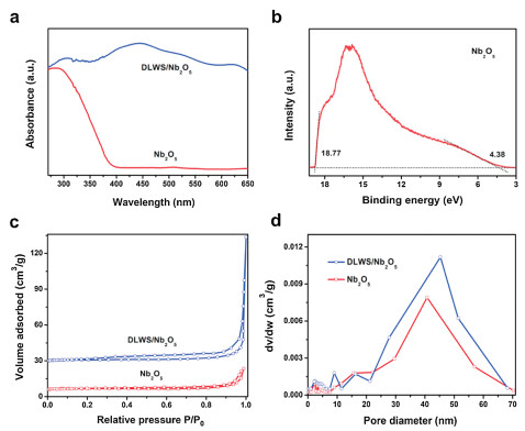
To unravel the dominating factors related to the excellent photocatalytic H2 evolution activity of double-layer WS2/Nb2O5 photocatalyst with the well-designed 2D/2D shell/core interface, diverse properties of DLWS/Nb2O5 including optics, texture and photoelectricity were investigated. In the UV–vis diffuse reflectance spectra (DRS, Fig. 4a), Nb2O5 shows an absorption in ultraviolet region with a calculated band-gap energy (Eg) of 3.15 eV. With the construction of 2D/2D shell/core interface, DLWS/Nb2O5 displays dramatically enhanced optical absorption both in ultraviolet and visible regions due to the effect of WS2 shell [36, 37], as evidenced by the incident photon-to-current conversion efficiency (IPCE) values of Nb2O5 and DLWS/Nb2O5 in Fig. S6 (Supporting information). The ultraviolet photoelectron spectroscopy (UPS) was performed to investigate the energy band structure of Nb2O5. As shown in Fig. 4b, based on the UPS curve with an excitation energy of 21.22 eV, the valence band energy (Ev) and conduction band energy (Ec) concerning the vacuum level of Nb2O5 are calculated to be −6.83 eV and −3.68 eV, respectively. According to the reference standard that 0 V versus normal hydrogen electrode (NHE) equals −4.44 eV versus the vacuum level, the Ev and Ec of Nb2O5 regarding the NHE are equal to 2.39 V and −0.76 V, respectively. Additionally, to acquire the texture information of Nb2O5 and DLWS/Nb2O5, the N2 adsorption-desorption isotherms were measured. As displayed in Fig. 4c, Nb2O5 and DLWS/Nb2O5 show the IV adsorption-desorption isotherm of N2 with the H3-type hysteresis loop, indicating the presence of mesopores. This result is well evidenced by the pore-size distributions in Fig. 4d, where both Nb2O5 and DLWS/Nb2O5 exhibit a pore-size distribution in the region of 2−70 nm, suggesting the coexistence of massive mesopores and a small amount of macropores. The specific surface area and pore volume of Nb2O5 and DLWS/Nb2O5 are listed in Table S1 (Supporting information). As shown in Table S1, DLWS/Nb2O5 exhibits increased specific surface area (14.48 m2/g) and pore volume (0.11 cm3/g) in comparison with those of Nb2O5 (6.65 m2/g and 0.03 cm3/g, respectively), which is due to the building of 2D/2D shell/core interface.

|
Download:
|
| Fig. 4. (a) UV–vis diffuse reflectance spectra of Nb2O5 and DLWS/Nb2O5. (b) UPS spectra of Nb2O5. (c) Nitrogen adsorption-desorption isotherms and (d) pore-size distributions of Nb2O5 and DLWS/Nb2O5. | |
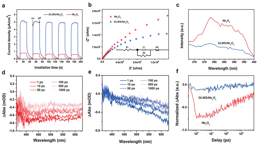
In order to investigate the separation and transfer nature of charges, transient photocurrent responses of Nb2O5 and DLWS/Nb2O5 were detected. As displayed in Fig. 5a, DLWS/Nb2O5 displays a high photocurrent density of 5.19 μA/cm2, up to 6.33 times higher than that of Nb2O5 (0.82 μA/cm2), suggestive of significantly accelerated charge separation and transfer [38-41]. This result is evidenced by electrochemical impedance spectroscopy (EIS, Fig. 5b) and photoluminescence (PL) spectra (Fig. 5c), where DLWS/Nb2O5 displays a smaller radius of Nyquist circle and a far lower emission peak intensity compared to Nb2O5, indicating the advantages of 2D/2D shell/core interface on accelerating charge migration [42-45]. Additionally, femtosecond-resolved transient absorption spectroscopy (TAS) is powerful technique for probing the charge separation and transfer. Figs. 5d and e exhibit the ultrafast TAS spectra of Nb2O5 and DLWS/Nb2O5 at select time points from 1 ps to 1000 ps. These spectra display broad negative induced absorption features from 360 nm to 630 nm, which are ascribed to the effect of overlapping electron and hole absorption in Nb2O5 [46]. The TAS kinetics at 380−410 nm is used to probe the lifetime of charge carriers (Fig. 5f). The relative lifetimes of charge carriers were obtained by fitting the kinetics with three-exponential decay functions. As shown in Table S2 (Supporting information), the average lifetime of charge carriers for DLWS/Nb2O5 (180.97 ps) is considerably shortened in comparison with that of Nb2O5 (230.50 ps), indicating fast charge transfer from Nb2O5 to WS2 via the well-designed 2D/2D shell/core interface [47−50], which is consistent with the time-resolved fluorescence decay spectra results (Fig. S7 and Table S3 in Supporting information).

|
Download:
|
| Fig. 5. (a) Transient photocurrent responses of Nb2O5 and DLWS/Nb2O5. (b) EIS Nyquist plots of Nb2O5 and DLWS/Nb2O5. The inset in (b) displays the impedance equivalent circuit. (c) PL spectra of Nb2O5 and DLWS/Nb2O5. Femtosecond-resolved TAS spectra of (d) Nb2O5 and (e) DLWS/Nb2O5. (f) TAS kinetics probed at 380–410 nm for Nb2O5 and DLWS/Nb2O5. | |
According to all results presented above, an underlying mechanism regarding the charge transfer in 2D/2D atomic double-layer WS2/Nb2O5 shell/core nanosheet for photocatalytic H2 evolution has been proposed. According to the UV–vis DRS and UPS results, Nb2O5 nanosheet can be excited to generate the photoexcited electron-hole pairs under simulated solar-light irradiation (λ ≥ 300 nm). The photoexcited electrons of Nb2O5 are rapidly injected into its conduction band (CB), while the photoexcited holes remained in its valence band (VB) are consumed by the hole-scavenger of triethanolamine. Owing to the presence of unusual 2D/2D shell/core interface with the large contact area, the photoexcited electrons on the CB of Nb2O5 can fast transfer to the atomic double-layer WS2 shell in time, thus boosting the charge separation and migration efficiency significantly (Fig. 5). Moreover, the unique atomic double-layer WS2 cocatalyst endows DLWS/Nb2O5 with the increased specific surface area to provide massive exposed active edges and sites (Fig. 4c and Table S1), where the electrons can reduce the H+ in aqueous solution to generate H2. The synergetic effect of significantly accelerated charge transfer and enhanced specific surface area leads to high photocatalytic H2 evolution activity of DLWS/Nb2O5.
In summary, 2D/2D atomic double-layer WS2/Nb2O5 shell/core nanosheet was successfully synthesized using a new in-situ vapor-phase growth method. Through the results of atom-resolved HAADF-STEM and HRTEM images, we reveal the presence of unique 2D/2D shell/core interface in DLWS/Nb2O5. According to the femtosecond-resolved ultrafast TAS spectra, we unravel fast charge transfer from Nb2O5 to atomic double-layer WS2, which leads to a high photocatalytic H2 generation rate of 237.6 μmol/h for DLWS/Nb2O5, up to 10.8 times by contrast with that of Nb2O5 nanosheet.
Declaration of competing interestThe authors declare no conflict of interest.
AcknowledgementsThis work was funded by the China Postdoctoral Science Foundation (pre-station, No. 2019TQ0050), Applied Basic Research Program of Sichuan Province (No. 2020YJ0068), the China Postdoctoral Science Foundation (No. 2020M673186), National Natural Science Foundation of China (No. 22002014), National Natural Science Foundation of China (No. 11804248), Natural Science Foundation of Tianjin (No. 18JCQNJC03200). Thanks for the technical help from Sichuan Province Key Laboratory of Display Science and Technology, State key Laboratory of Electronic Thin Films and Integrated Devices. This work is also supported by MOE Tier 1 RG4/17 and MOE Tier 2 MOE2019-T2-2-105. Dr. Dan Tian gratefully acknowledged the financial support from the National Natural Science Foundation of China (No. 21971113).
Appendix A. Supplementary dataSupplementary material related to this article can be found, in the online version, at doi:https://doi.org/10.1016/j.cclet.2021.03.057.
| [1] |
X. Wang, L. Chen, S.Y. Chong, et al., Nat. Chem. 10 (2018) 1180-1189. DOI:10.1038/s41557-018-0141-5 |
| [2] |
J. Kosco, M. Bidwell, H. Cha, et al., Nat. Mater. 19 (2020) 559-565. DOI:10.1038/s41563-019-0591-1 |
| [3] |
J. Di, J. Xiong, H. Li, Z. Liu, Adv. Mater. 30 (2018) 1704548. DOI:10.1002/adma.201704548 |
| [4] |
W. Bi, X. Li, L. Zhang, et al., Nat. Commun. 6 (2015) 8647. DOI:10.1038/ncomms9647 |
| [5] |
S. Bai, L. Yang, C. Wang, et al., Angew. Chem. Int. Ed. 54 (2015) 14810-14814. DOI:10.1002/anie.201508024 |
| [6] |
G. Zhao, Y. Sun, W. Zhou, et al., Adv. Mater. 29 (2017) 1703258. DOI:10.1002/adma.201703258 |
| [7] |
D. Zheng, X.N. Cao, X. Wang, Angew. Chem. Int. Ed. 55 (2016) 11512-11516. DOI:10.1002/anie.201606102 |
| [8] |
B. Lin, J. Li, B. Xu, et al., Appl. Catal. B: Environ. 243 (2019) 94-105. DOI:10.1016/j.apcatb.2018.10.029 |
| [9] |
T. Su, Q. Shao, Z. Qin, Z. Guo, Z. Wu, ACS Catal. 8 (2018) 2253-2276. DOI:10.1021/acscatal.7b03437 |
| [10] |
B. Lin, H. Li, H. An, et al., Appl. Catal. B: Environ. 220 (2018) 542-552. DOI:10.1016/j.apcatb.2017.08.071 |
| [11] |
Y.J. Yuan, D. Chen, J. Zhong, et al., J. Mater. Chem. A 5 (2017) 15771-15779. DOI:10.1039/C7TA04410K |
| [12] |
Y. Li, X. Xu, J. Wang, et al., Appl. Catal. B: Environ. 270 (2020) 118855. DOI:10.1016/j.apcatb.2020.118855 |
| [13] |
J. Xiong, L. Wen, F. Jiang, et al., J. Mater. Chem. A 3 (2015) 20627-20632. DOI:10.1039/C5TA04755B |
| [14] |
Y. Zhou, E. Song, J. Zhou, et al., ACS Nano 12 (2018) 4486-4493. DOI:10.1021/acsnano.8b00693 |
| [15] |
J. Yu, S. Seo, Y. Luo, et al., ACS Nano 14 (2020) 1715-1726. DOI:10.1021/acsnano.9b07366 |
| [16] |
J. McAllister, N.A.G. Bandeira, J.C. McGlynn, et al., Nat. Commun. 10 (2019) 370. DOI:10.1038/s41467-018-08208-4 |
| [17] |
J. Zhou, J. Lin, X. Huang, et al., Nature 556 (2018) 355-359. DOI:10.1038/s41586-018-0008-3 |
| [18] |
X. Xu, F. Luo, W. Tang, et al., Adv. Funct. Mater. 28 (2018) 1804055. DOI:10.1002/adfm.201804055 |
| [19] |
X. Yan, M. Xia, B. Xu, et al., Appl. Catal. B: Environ. 232 (2018) 481-491. DOI:10.1016/j.apcatb.2018.03.068 |
| [20] |
K. Tang, X. Wang, Q. Li, C. Yan, Adv. Mater. 30 (2017) 1704779. |
| [21] |
M. Zhu, C. Zhai, M. Fujitsuka, T. Majima, Appl. Catal. B: Environ. 221 (2018) 645-651. DOI:10.1016/j.apcatb.2017.09.063 |
| [22] |
J. Duan, S. Chen, B.A. Chambers, G.G. Andersson, S.Z. Qiao, Adv. Mater. 27 (2015) 4234-4241. DOI:10.1002/adma.201501692 |
| [23] |
B. Mahler, V. Hoepfner, K. Liao, G.A. Ozin, J. Am. Chem. Soc. 136 (2014) 14121-14127. DOI:10.1021/ja506261t |
| [24] |
Mayorga-Martinez C.C., A. Ambrosi, A.Y.S. Eng, Z. Sofer, M. Pumera, Adv. Funct. Mater. 25 (2015) 5611-5616. DOI:10.1002/adfm.201502223 |
| [25] |
X.J. Chua, J. Luxa, A.Y.S. Eng, et al., ACS Catal. 6 (2016) 5724-5734. DOI:10.1021/acscatal.6b01593 |
| [26] |
B. Lin, Z. Chen, P. Song, et al., Small 16 (2020) 2003302. DOI:10.1002/smll.202003302 |
| [27] |
G.T.S.T.D. Silva, K.T.G. Carvalho, O.F. Lopes, C. Ribeiro, Appl. Catal. B: Environ. 216 (2017) 70-79. DOI:10.1016/j.apcatb.2017.05.038 |
| [28] |
S. Zhang, S. Chen, D. Liu, J. Zhang, T. Peng, Appl. Surf. Sci. 529 (2020) 147013. DOI:10.1016/j.apsusc.2020.147013 |
| [29] |
L. Yao, D. Wei, D. Yan, C. Hu, Chem. Asian J. 10 (2015) 630-636. DOI:10.1002/asia.201403387 |
| [30] |
B. Lin, A. Chaturvedi, J. Di, et al., Nano Energy 76 (2020) 104972. DOI:10.1016/j.nanoen.2020.104972 |
| [31] |
H. An, B. Lin, C. Xue, et al., Chinese J. Catal. 39 (2018) 654-663. DOI:10.1016/S1872-2067(17)62927-9 |
| [32] |
F. He, A. Meng, B. Cheng, W. Ho, J. Yu, Chin. J. Catal. 41 (2020) 9-20. DOI:10.1016/S1872-2067(19)63382-6 |
| [33] |
D. Spanu, S. Recchia, S. Mohajernia, et al., ACS Catal. 8 (2018) 5298-5305. DOI:10.1021/acscatal.8b01190 |
| [34] |
H. Li, P. Wang, X. Yi, H. Yu, Appl. Catal. B: Environ. 264 (2020) 118504. DOI:10.1016/j.apcatb.2019.118504 |
| [35] |
Z. Zhang, K. Liu, Y. Bao, B. Dong, Appl. Catal. B: Environ. 203 (2017) 599-606. DOI:10.1016/j.apcatb.2016.10.064 |
| [36] |
C. Xue, P. Zhang, G. Shao, G. Yang, Chem. Eng. J. 398 (2020) 125602. DOI:10.1016/j.cej.2020.125602 |
| [37] |
Y. Tang, W. He, Y. Lu, et al., J. Phys. Chem. C 118 (2014) 25365-25373. DOI:10.1021/jp5092174 |
| [38] |
B. Lin, H. An, X. Yan, et al., Appl. Catal. B: Environ. 210 (2017) 173-183. DOI:10.1016/j.apcatb.2017.03.066 |
| [39] |
J. Di, J. Xia, M.F. Chisholm, et al., Adv. Mater. 31 (2019) 1807576. DOI:10.1002/adma.201807576 |
| [40] |
B. Lin, Y. Zhou, B. Xu, et al., Mater. Horiz. 8 (2021) 612-618. DOI:10.1039/D0MH01693D |
| [41] |
L. Yao, D. Wei, Y. Ni, D. Yan, C. Hu, Nano Energy 26 (2016) 248-256. DOI:10.1016/j.nanoen.2016.05.031 |
| [42] |
Y. Zhou, J. Zhang, E. Song, et al., Nat. Commun. 11 (2020) 2253. DOI:10.1038/s41467-020-16111-0 |
| [43] |
C. Xue, H. An, G. Shao, G. Yang, Chinese J. Catal. 42 (2021) 583-594. DOI:10.1016/S1872-2067(20)63649-X |
| [44] |
X. Fang, R. Gao, Y. Yang, D. Yan, iScience 16 (2019) 22-30. DOI:10.1016/j.isci.2019.05.015 |
| [45] |
M. Arif, G. Yasin, M. Shakeel, et al., J. Energy Chem. 58 (2021) 237-246. DOI:10.1016/j.jechem.2020.10.014 |
| [46] |
K.L. Corp, C.W. Schlenker, J. Am. Chem. Soc. 139 (2017) 7904-7912. DOI:10.1021/jacs.7b02869 |
| [47] |
P. Wang, Y. Mao, L. Li, et al., Angew. Chem. Int. Ed. 58 (2019) 11329-11334. DOI:10.1002/anie.201904571 |
| [48] |
Y. Mao, P. Wang, L. Li, et al., Angew. Chem. Int. Ed. 59 (2020) 3685-3690. DOI:10.1002/anie.201914001 |
| [49] |
B. Lin, G. Yang, L. Wang, Angew. Chem. Int. Ed. 58 (2019) 4587-4591. DOI:10.1002/anie.201814360 |
| [50] |
J. Di, C. Chen, S.Z. Yang, et al., Nat. Commun. 10 (2019) 2840. DOI:10.1038/s41467-019-10392-w |