 2021, Vol. 32


b National Institute for Advanced Materials, Nankai University, Tianjin 300350, China;
c Tianjin Key Laboratory for Rare Earth Materials and Applications, Nankai University, Tianjin 300350, China
Two-dimensional (2D) materials are competitive candidates for next-generation electronic and optoelectronic devices. Their flat surfaces free of dangling bonds, atomically thin thicknesses, and high carrier mobilities bring merits of efficient channel current regulation and a high degree of vertical integration of different types of 2D materials [1-5]. The past decade has witnessed an extraordinary increase in the family of 2D materials including graphene [6-8], black phosphorus (BP) [9-11], and transition metal dichalcogenides (TMDs) [12, 13]. However, in these 2D materials, graphene is difficult to be switched off [14, 15], TMDs generally have low carrier mobilities [3, 16, 17], and BP is not air-stable [18, 19], Thus, it is urgent to find new type of 2D materials with high carrier mobilities, suitable band gaps, and good ambient stability simultaneously. Bi2O2Se has recently emerged as a bismuth-based oxychalcogenide 2D material, which shows a tetragonal structure with the I4/mmm space group. It consists of planar covalently bonded oxide layers (Bi2O2) weakly connected by Se square arrays [20]. With the advantages of high carrier mobility (> 20, 000 cm2 V−1 s−1 at 2K), layer-number tunable band gaps, low subthreshold swing (SS, ~65 mV/dec) [21, 22] and air stability, it is particularly suitable for high-performance transistors or photodetectors.
While bulk Bi2O2Se was synthesized by solid-state reaction as early as 1973 [23], the recent syntheses of Bi2O2Se ultrathin films with controlled thicknesses, good crystallinity and large sizes via chemical vapor deposition (CVD) have spurred the fundamental studies of their properties and applications [21]. However, CVD approaches typically suffer from the disadvantages of low product yield, high equipment investment, as well as the complex and strict technical processes. In addition, complicated transfer steps are necessary if different substrates are needed for device fabrications, which makes it difficult for large-scale integration. The wet chemistry synthesis of Bi2O2Se has emerged as an alternative mass-production approach with benefits of mild conditions, controllability, inexpensiveness, and high yield. For example, Bi2O2Se nanosheets with thicknesses of 155 nm and clear edges have been produced by a molten salt hydrothermal method [24]; Bi2O2Se nanosheets with thicknesses of 2 nm and lateral sizes of 100 − 200 nm have been produced by reacting selenourea with bismuth nitrate in alkaline solutions at room temperature [25]. A recent work also illustrates the importance of organic ions on the thicknesses of Bi2O2Se nanosheets during hydrothermal reactions [26]. These methods are simple and feasible on a large scale, but the synthesized products typically have inhomogeneous distributions in thicknesses or sizes, and tend to agglomerate due to the absence of stabilizing ligands.
Here, we propose a new synthesis method to better control the phase and the morphology of Bi2O2Se nanosheets by separating the generation of seed crystals and the growth of nanosheets. We have systematically studied the influence of different solvents, additives and reaction conditions on the sizes and morphologies of Bi2O2Se nanosheets. The large and ultrathin nanosheets attained at optimized conditions are further assembled into thin films by electrostatic assembly. Using these thin films, we fabricate high performance photodetectors with responsivity of ~6.1 A/W and response time of ~368 μs, which are superior to those prepared by other solution-processed Bi2O2Se nanosheets, or even those synthesized by CVD [26-31]. The preparation and assembly of colloidal Bi2O2Se nanosheets are of great significance to the practical realization of thin film 2D materials for future electronic applications.
To better control the synthesis of Bi2O2Se nanosheets, the seeding and growing steps are separated in our procedure, which is schematically shown in Fig. 1. The overall reaction in the seeding step is shown as follows:
|
(1) |

|
(2) |

|
(3) |

|
Download:
|
| Fig. 1. Schematic diagram of a two-step synthesis process of the Bi2O2Se nanosheets. | |
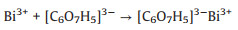
The citrate anions ([C6O7H5]3−) released by the dissolution of sodium citrate are chelated with Bi3+ to produce [C6O7H5]3−Bi3+ complexes in solution 1 (Eq. 1) [32, 33]. The selenide ions (Se2−) from the decomposition of selenourea (SeC(NH2)2) in alkaline medium are produced along with cyanamide (H2NCN) in solution 2 (Eq. 2). When the bismuth nitrate solution is added dropwise to the selenourea solution, Bi3+ slowly released from the complexes react with H2O and Se2− to form Bi2O2Se seeds through a thermodynamically favorable process (Eq. 3). The as-synthesized seeds have a morphology of round disk with an average diameter of 5.5±0.6 nm by TEM (Fig. 2a).

|
Download:
|
| Fig. 2. Morphologies and characterizations of the synthesized Bi2O2Se nanosheets. TEM images of (a) crystal seeds after mixing Solution 1 and 2, and (b) Bi2O2Se nanosheets. (c) High-resolution TEM image of the Bi2O2Se nanosheets, along with an inset SAED pattern demonstrating its single crystalline nature. (d) AFM image of the multiple Bi2O2Se nanosheets and the height profile with a thickness of 10 nm. (e) XRD pattern of the synthesized Bi2O2Se nanosheets. (f) Relationship between the rescaled absorption factor (αhν)1/2 and the photon energy hν, showing a fitted optical band gap of 0.9 eV. | |
In the subsequent growth step, the seeds undergo Ostwald ripening [34] in the hydrothermal conditions at 150 ℃, and grow laterally into Bi2O2Se nanosheets with a size as large as ~1.4 μm after 6h (Fig. 2b). The Bi2O2Se nanosheets are further analyzed by high-resolution TEM and selected-area electron diffraction (SAED) to confirm the crystallinity. As shown in Fig. 2c, the high-resolution TEM image shows a lattice spacing of 0.27 nm, corresponding to the plane (110) of Bi2O2Se, and the strong SAED pattern (Fig. 2c inset) indicates the single crystalline nature of the as-synthesized nanosheets. The AFM measurements reveal an average thickness of 10 nm, indicating a multilayer structure (Fig. 2d). Furthermore, Fig. 2e depicts a typical XRD pattern congruent with tetragonal structure (JCPDS No. 25-1463). The diffraction peaks at 32.253° and 46.061° correspond to the crystal planes of (110) and (020) denoted in Fig. 2c. No impurity peaks are observed according to the standard card, which indicates that the crystalline Bi2O2Se are of single phase and high purity. The optical properties of the as-prepared Bi2O2Se nanosheets are also characterized. As seen from Fig. S1 (Supporting information), the UV–vis-NIR absorption spectrum measured from a diluted Bi2O2Se solution shows strong absorbance in the entire visible light region, and is extended to the region of long wavelength with a decreased absorption. The band gap of the Bi2O2Se nanosheets can be estimated according to the equation (αhν)1/2 = A·(hν − Eg), where α is the absorption coefficient, hν is the photon energy, A is a constant, and Eg is the band gap energy. Following the absorption spectrum, the dependence of (αhν)1/2 on hν is derived and shown in Fig. 2f, which results in a band gap (Eg) of 0.9 eV. All these characterization results confirm that the Bi2O2Se nanosheets are successfully synthesized.
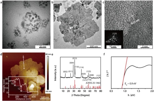
To explore the effect of solvents, several other solvents are used to substitute ethylene glycol in the synthesis. Figs. 3a–d show the TEM images of the Bi2O2Se nanosheets synthesized in different solvents (Samples 1 − 4). The yielded Bi2O2Se nanosheets have a small lateral size of ~60 nm (Sample 1, Fig. 3a) when the DI water is used in Solution 1. In comparison, their sizes increase to ~200 nm (Sample 2, Fig. 3b) or ~300 nm (Sample 3, Fig. 3c) when 0.78 mol/L HNO3 or 0.5 mol/L mannitol in DI water is used as the solvent in Solution 1. The use of ethylene glycol in Solution 1 further enlarges the lateral size of Bi2O2Se nanosheets to over 1 μm (Sample 4, Fig. 3d). It is likely that Bi3+ is more stable when HNO3, mannitol, or ethylene glycol are added to reduce the competing hydrolysis of Bi3+ in water [34]. The more stable solution is beneficial to the growth of nanosheets in the subsequent hydrothermal process. In addition, the high viscosity of ethylene glycol reduces the collision frequency of the ions, leading to less number of seeds in the solution for larger nanosheets [35]. XRD characterizations are used to inspect the phase purity of these four products. As shown in Fig. 3e, the XRD patterns for the samples of different solvent systems (Samples 1, 2 and 4) match well with that of tetragonal Bi2O2Se (JCPDS No. 25-1463), while Sample 3 has some impurities inside. It is observed that the intensities of the diffraction peaks increase with the increased lateral size of nanosheets, indicating the improved crystallinity. Furthermore, the electrical conductivities are measured for compacted films of Bi2O2Se nanosheets from Samples 1−4 (Fig. 3f, see the inset for the schematic diagram of measurement setup). It is shown that the conductivities increase with the increasing size of nanosheets for Samples 1, 2 and 4. Sample 3 has a lower conductivity than Sample 2 despite its sizes, which is owing to the impurities in the products.

|
Download:
|
| Fig. 3. Characterizations of the Bi2O2Se nanosheets by tuning the solvents. Morphology of the Bi2O2Se nanosheets obtained from the solvent of (a) water (Sample 1), (b) HNO3 solution (Sample 2), (c) mannitol solution (Sample 3), and (d) the mixture of ethylene glycol and water (Sample 4). (e) XRD patterns of the Bi2O2Se nanosheets in Samples 1–4. (f) Electrical conductivity of four compacted samples of Bi2O2Se nanosheets. Inset: A schematic diagram for measurement. | |
The reaction time and temperatures are also tuned to investigate the optimum conditions for the control of the morphologies and the sizes of Bi2O2Se nanosheets. Fig. S2a (Supporting information) shows the dependence of the lateral sizes of nanosheets on the different reaction time, while other conditions are kept the same. When the reaction time is 4h, the lateral sizes of most nanosheets are ~700 nm or less (Fig. S3a in Supporting information); when the reaction time is increased to 6h, the nanosheets can grow to a size of ~1.4 μm (Fig. S3b in Supporting information); when the time is extended to 8h, the continual growth of nanosheets lead to their aggregation into small bumps or even precipitation, therefore the large-sized nanosheets appear rare in the final dispersion (Fig. S3 c in Supporting information). As to the reaction temperature, it has complicated effects on the formation of nanosheets. It is observed that the lateral sizes of the nanosheets synthesized at 120 ℃ and 180 ℃ are much smaller than those of the nanosheets synthesized at 150 ℃ (Figs. S2b and S4 in Supporting information). The formation of Bi2O2Se nanosheets is a thermodynamically controlled process. At a relatively low temperature (120 ℃), the reaction rate is very slow, making the nanosheets unable to grow sufficiently; on the other hand, a high temperature (180 ℃) makes lateral growth of nanosheets unfavorable due to the increased activity of other crystalline facets. The above discussion shows that an appropriate selection of the reaction time and temperature can promote the growth of nanosheets.
We further study the effect of the amounts of different reactants (NaOH or sodium citrate), or the volume ratio of ethylene glycol and water to understand their effects in the reaction. The increased addition of NaOH from 300 mg to 600 mg leads to less homogenous distribution of sizes, and a drawback of aggregation of nanosheets (Figs. S2c and S5 in Supporting information). As a conventional mineralizer, an appropriate amount of sodium hydroxide can not only promote the reaction rate, but also has an important effect on the morphology of the products [5, 36, 37]. But excessive amount of sodium hydroxide accelerates crystal nucleation, resulting in an increase in nucleation sites and a decrease in the size of nanosheets. The coordination agent sodium citrate is also related to the formation of Bi2O2Se nanosheets (Fig. S2d in Supporting information). Without any sodium citrate in the reaction, Bi2O2Se nanosheets of small sizes are obtained (Fig. S6a in Supporting information); when 2.7 mmol of sodium citrate is added, micron-sized nanosheets are formed (Fig. S6b in Supporting information); when 4.1 mmol of sodium citrate is added, the size of nanosheets decrease (Fig. S6 c in Supporting information). In the reaction, sodium citrate chelates with Bi3+ to form a stable metal complex, and varying amounts of sodium citrate regulate the concentration of free Bi3+ in the system to balance the coordination and dissolution equilibriums, and further regulate the reaction rate and grain growth [33, 38]. The volume ratio of ethylene glycol to water also affects the synthesis of Bi2O2Se nanosheets. The optimal ratio is 1:1 with favorable production of high quality and pure phase Bi2O2Se nanosheets (Figs. S2e and S7 in Supporting information). If the ratio is larger than 1, products of Bi2O2Se and Bi2Se3 are harvested (Fig. S7d in Supporting information) with a lateral size decrease (Figs. S7b and c in Supporting information) due to the reduced viscosity of the system. All the above discussions demonstrate that the sizes and morphologies of Bi2O2Se nanosheets are affected by a series of reaction conditions.
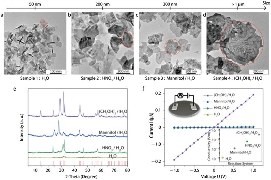
A high-quality thin film of the Bi2O2Se nanosheets obtained at optimum reaction conditions is constructed by electrostatic assembly (Fig. 4a). In a typical process, a pretreated substrate is immersed in a positively charged PDDA solution, and then the water dispersion of Bi2O2Se nanosheets (for more details, see Experimental Section in Supporting information). Bi2O2Se nanosheets are supposed to have negative charges due to the stabilizing citrate ligands, which is verified by the measured surface charge potential of −39.3 mV (Fig. S8 in Supporting information). This large negative surface potential also ensures the great stability of Bi2O2Se nanosheets in water. The Bi2O2Se nanosheets can be dispersed in the DI water for at least one day (Fig. S8). The optical image in Fig. 4b shows that the Bi2O2Se nanosheets are densely assembled on the SiO2/Si substrate, forming a uniform film without localized aggregation.

|
Download:
|
| Fig. 4. Thin-film assembly and photodetectors of Bi2O2Se nanosheets. (a) Schematic diagram of the electrostatic assembly process for Bi2O2Se thin films. (b) Optical image of the prepared Bi2O2Se thin film after the deposition of metal electrodes. (c) Schematic for Bi2O2Se thin-film photodetectors under a 520-nm laser illumination and the electrical connections for measurements. | |
This film is then used to fabricate two-terminal photodetectors by typical photolithography processes. The distance between two contact electrodes is kept at 10 μm in the devices. A schematic diagram of the device in the photoelectric experiment is shown in Fig. 4c. The current-voltage (Ⅰ–Ⅴ) characteristics of the Bi2O2Se films are measured (Fig. 5a). In a dark environment, the original resistance of the sample is about 72.8MΩ estimated from the current measured at 10 V (Fig. 5a). Under the 520 nm laser irradiation, the Ⅰ-Ⅴ characteristics have changed significantly, and the current is greater than 52 μA at 10 V (Fig. 5a). The dark currents are recovered after the laser is off (Fig. 5a). The photocurrent ΔI is calculated as the variation between the current with and without laser irradiation, i.e., ΔI = Iph − Idark. A series of photoelectric measurements are then conducted to characterize the responsiveness of Bi2O2Se thin films. In Fig. 5b, the time-dependent characterizations are obtained, shown in the form of normalized photocurrent (ΔI/ΔImax) versus time. When the laser is turned on at t = 0, the photocurrent rises sharply from the background current (ΔI/ΔImax = 0) and rises to the maximum current (ΔI/ΔImax = 1) within 0.5s. The time of the rising edge is approximately 368 μs (rise time tr, 0%–80%). At the same time, the photocurrent decreases when the laser is turned off. It takes about 592 μs during the decay edge (decay time td, 100% to 20%), which is slightly longer than the rising edge. Both tr and td are very short with a magnitude of 102 μs, therefore the photoelectric curves in Fig. 5b are close to a perfect rectangle, exhibiting good photoelectric performances. These response properties, especially the fast response speed, can be attributed to the large sizes of nanosheets and small number of electronic traps in the Bi2O2Se films.

|
Download:
|
| Fig. 5. Photoelectric performances of the Bi2O2Se photodetectors. (a) I-V characteristics of the Bi2O2Se films with (red balls) and without (blue boxes) a laser illumination, in comparison to that of the initial state (black squares). (b) The time-resolved photoelectric response curve under a laser illumination for 0.5s and a bias of 10 V. (c) Multi-periodic response curves with a variation of laser power illumination: 1.6, 4.5, 9, 13, 17, 22, 26, 30, 33, 37, 40 and 42 mW. Top: A series of square waves at 1 Hz of the signal generator. (d) Power density (P) dependence of the photocurrent (ΔI) in Bi2O2Se samples. The experimental points are fitted following a linear and a nonlinear power law ΔI ~, which are α = 1 (dashed black line) and α = 0.71 (solid blue line), respectively. (e) Correlation of the normalized response and the frequency, showing a −3 dB bandwidth at ~1 kHz. (f) Performance comparison of thin-film photodetectors based on different 2D materials synthesized by solution methods [39]. | |
Furthermore, the multi-periodic dynamic response performance of the Bi2O2Se film is studied, and it shows a high and fast photoelectric responsiveness. As shown in Fig. 5c, the power received by the sample increased from 1.6 mW to 42 mW under the 1-Hz modulated laser irradiation. The recorded current gives a response to the modulated laser (Fig. 5c, bottom panel), which corresponds to the applied square wave signals (Fig. 5c, top panel). According to the results in Fig. 5c, the parameter of responsivity R can be calculated by dividing the variation in current (photocurrent, ΔI) by the total power received on the effective area R = ΔI/(A × P), where the power density P is the laser power per unit area, the unit is mW/cm2 (laser power diameter is about 1 mm), and the effective area A is 10 μm × 120 μm. Therefore, the power density dependence of the photocurrent is shown in Fig. 5d. According to the linear fitting result, the calculated responsivity R is 6.1 A/W (dashed black line, Fig. 5d). A detailed study of the power law of Bi2O2Se thin film shows that the photocurrent follows a sub-linear relationship with light density, ΔI ~ P, where α = 0.71 (Fig. 5d). This phenomenon mainly originates from the saturation absorption of Bi2O2Se samples, and has been observed in photodetectors using several other low-dimensional semiconductors [27]. On the other hand, the slight nonlinearity in the power law is caused by carrier recombination via the defects and charge impurities within or between the nanosheets. Although the solution-processed Bi2O2Se nanosheets have more defects and imperfections than those materials synthesized by CVD or by mechanical exfoliation, they are still potential candidates for high performance photodetectors.
Our Bi2O2Se thin film photodetectors also have a high-frequency response performance (Fig. 5e and Fig. S9 in Supporting information). Fig. S9 shows the measured voltage response from the current amplifier when the photodetectors are under the different laser modulation frequencies from 0.2 Hz to 100 kHz. When the modulation frequency is low (0.2 Hz − 20 Hz), the response curve is displayed as a rectangle (Figs. S9a−d). Similar to Fig. 5b, the rising edge is always faster than the decay edge, and rise/decay time are around hundreds of microseconds. As the modulation frequency increases, slight distortions tend to appear on the curve, but the response amplitude value remains at a similar level to that at relatively low frequencies until it reaches 102 Hz (Figs. S9e−g). When the frequency is higher than a kilohertz (103 Hz), the response curve changes from a rectangle to a distorted rectangle (Figs. S8h−j). When the frequency is as high as 10 kHz or more, the response curve looks like a triangle (Figs. S9k−m). Finally, the response behavior can still be distinguished at 100 kHz (Fig. S9 n). Based on these results, we plot the correlation between the normalized responses and the modulation frequency f, as shown in Fig. 5e. The normalized response is given by 20 × lg(R/Rmax) in dB, where Rmax is regarded as the responsivity obtained at f = 0.2 Hz. The typical parameter is the −3 dB bandwidth at f = 1 kHz, at which the response drops to 70.8% of the maximum value. Then, the time constant τ can be estimated from the −3 dB frequency using the general relationship: τ ~ 0.35 / f−3 dB, thus τ ~ 350 μs. It is very close to the time constants of 368 μs (tr) and 592 μs (td) obtained from the direct measurement results in Fig. 5b. Compared with other 2D materials prepared by solution methods (Fig. 5f), our Bi2O2Se photodetectors have higher and faster response. This observation may be due to the large sizes of nanosheets in the films, which allow the photogenerated carriers to move easily. Therefore, we provide a large-scale and low-cost way to develop high-performance photodetectors in large-scale but low-cost production based on the assembled films of colloidal Bi2O2Se nanosheets.
In conclusion, we have successfully synthesized the micron-scale and ultrathin Bi2O2Se nanosheets through a two-step colloidal synthesis route. A variety of experimental variables have been studied to reveal the roles of reagents in the reaction and related mechanisms in the formation of Bi2O2Se nanosheets. The precise control of Bi2O2Se nanosheets with a lateral size greater than 1 μm and a thickness of 10 nm has been achieved in optimum conditions. Electrostatic assembly is used to fabricate the high-quality thin films of Bi2O2Se nanosheets, which are then applied for photodetectors. These devices have high photoresponsivity and short response time, and respond well to modulations up to 100 kHz. Such performance is superior to those of other devices prepared from solution-processed 2D materials. Our work provides a promising approach to the synthesis and assembly of Bi2O2Se nanosheets for high-performance photodetectors.
Declaration of competing interestThe authors report no declarations of interest.
AcknowledgmentsThe work was supported by National Science Foundations of China (Nos. 51873088, 12004195), Natural Science Foundations of Tianjin (No. 20JCQNJC01820), Tianjin Municipal Science and Technology Commission (No. 18JCZDJC38400), "111" Project of China's Higher Education (No. B18030), and Fundamental Research Funds for the Central Universities from Nankai University (No. 63201061).
Appendix A. Supplementary dataSupplementary material related to this article can be found, in the online version, at doi:https://doi.org/10.1016/j.cclet.2021.03.039.
| [1] |
M. Liu, X. Yin, E. Ulin-Avila, et al., Nature 474 (2011) 64-67. DOI:10.1038/nature10067 |
| [2] |
B. Radisavljevic, A. Radenovic, J. Brivio, V. Giacometti, A. Kis, Nat. Nanotechnol. 6 (2011) 147-150. DOI:10.1038/nnano.2010.279 |
| [3] |
Q.H. Wang, K. Kalantar-Zadeh, A. Kis, J.N. Coleman, M.S. Strano, Nat. Nanotechnol. 7 (2012) 699-712. DOI:10.1038/nnano.2012.193 |
| [4] |
F. Liu, W.L. Chow, X. He, et al., Adv. Funct. Mater. 25 (2015) 5865-5871. DOI:10.1002/adfm.201502316 |
| [5] |
J. Zhang, K. Huang, L. Yuan, S. Feng, Crystengcomm 20 (2018) 470-476. DOI:10.1039/C7CE01827D |
| [6] |
K.S. Novoselov, A.K. Geim, S.V. Morozov, et al., Science 306 (2004) 666-669. DOI:10.1126/science.1102896 |
| [7] |
T. Mueller, F. Xia, P. Avouris, Nat. Photonics 4 (2010) 297-301. DOI:10.1038/nphoton.2010.40 |
| [8] |
Y. Zhang, T. Liu, B. Meng, et al., Nat. Commun. 4 (2013) 1811. DOI:10.1109/TCPMT.2013.2281605 |
| [9] |
L. Li, Y. Yu, G.J. Ye, et al., Nat. Nanotechnol. 9 (2014) 372-377. DOI:10.1038/nnano.2014.35 |
| [10] |
Z. Zhang, L. Li, J. Horng, et al., Nano Lett. 17 (2017) 6097-6103. DOI:10.1021/acs.nanolett.7b02624 |
| [11] |
L. Li, W. Han, L. Pi, et al., Infomat 1 (2019) 54-73. DOI:10.1002/inf2.12005 |
| [12] |
K.F. Mak, J. Shan, Nat. Photonics 10 (2016) 216-226. DOI:10.1038/nphoton.2015.282 |
| [13] |
S.S. Wang, X.X. Chen, B. Huang, et al., CCS Chem 1 (2019) 448-454. DOI:10.31635/ccschem.019.20190012 |
| [14] |
W. Zhang, C.T. Lin, K.K. Liu, et al., ACS Nano 5 (2011) 7517-7524. DOI:10.1021/nn202463g |
| [15] |
C. Xie, Y. Wang, Z.X. Zhang, D. Wang, L.B. Luo, Nano Today 19 (2018) 41-83. DOI:10.1016/j.nantod.2018.02.009 |
| [16] |
Y. Shi, H. Li, L.J. Li, Chem. Soc. Rev. 44 (2015) 2744-2756. DOI:10.1039/C4CS00256C |
| [17] |
Z. Cai, B. Liu, X. Zou, H.M. Cheng, Chem. Rev. 118 (2018) 6091-6133. DOI:10.1021/acs.chemrev.7b00536 |
| [18] |
J.D. Wood, S.A. Wells, D. Jariwala, et al., Nano Lett. 14 (2014) 6964-6970. DOI:10.1021/nl5032293 |
| [19] |
X. Wang, Y. Sun, K. Liu, 2D Materials 6 (2019) 042001. DOI:10.1088/2053-1583/ab20d6 |
| [20] |
J. Wu, C. Tan, Z. Tan, et al., Nano Lett. 17 (2017) 3021-3026. DOI:10.1021/acs.nanolett.7b00335 |
| [21] |
J. Wu, H. Yuan, M. Meng, et al., Nat. Nanotechnol. 12 (2017) 530-534. DOI:10.1038/nnano.2017.43 |
| [22] |
J. Yin, Z. Tan, H. Hong, et al., Nat. Commun. 9 (2018) 3311. DOI:10.1038/s41467-018-05874-2 |
| [23] |
H. Boller, Monatshefte für Chem. 104 (1973) 916-919. DOI:10.1007/BF00903904 |
| [24] |
X. Tian, H. Luo, R. Wei, et al., Adv. Mater. 30 (2018) 1801021. DOI:10.1002/adma.201801021 |
| [25] |
T. Ghosh, M. Samanta, A. Vasdev, et al., Nano Lett. 19 (2019) 5703-5709. DOI:10.1021/acs.nanolett.9b02312 |
| [26] |
M.Q. Li, L.Y. Dang, G.G. Wang, et al., Adv. Mater. Technol. 5 (2020) 2000180. DOI:10.1002/admt.202000180 |
| [27] |
J. Li, Z. Wang, Y. Wen, et al., Adv. Funct. Mater. 28 (2018) 1706437. DOI:10.1002/adfm.201706437 |
| [28] |
Q. Fu, C. Zhu, X. Zhao, et al., Adv. Mater. 31 (2019) 1804945. DOI:10.1002/adma.201804945 |
| [29] |
U. Khan, Y. Luo, L. Tang, et al., Adv. Funct. Mater. 29 (2019) 1807979. DOI:10.1002/adfm.201807979 |
| [30] |
T. Tong, Y. Chen, S. Qin, et al., Adv. Funct. Mater. 29 (2019) 1905806. DOI:10.1002/adfm.201905806 |
| [31] |
Y. Sun, S. Ye, J. Zhang, et al., J. Mater. Chem. C 8 (2020) 14711-14717. DOI:10.1039/d0tc04352d |
| [32] |
K. Zhang, J. Liang, S. Wang, et al., Cryst. Growth Des. 12 (2012) 793-803. DOI:10.1021/cg201112j |
| [33] |
Y. Xu, S. Xu, S. Wang, Y. Zhang, G. Li, Dalton Trans. 43 (2014) 479-485. DOI:10.1039/C3DT52004H |
| [34] |
J. Xiong, G. Cheng, Z. Lu, et al., CrystEngComm 13 (2011) 2381-2390. DOI:10.1039/c0ce00705f |
| [35] |
H. Wang, Q. Lin, X. Dou, T. Yang, Y. Han, Crystals 7 (2017) 357. DOI:10.1007/978-3-319-68542-7_30 |
| [36] |
X. Wei, G. Xu, Z. Ren, G. Shen, G. Han, Mater. Lett. 62 (2008) 3719-3721. DOI:10.1016/j.matlet.2008.04.039 |
| [37] |
T. Ly, J. Wen, L.D. Marks, Nano Lett. 18 (2018) 5186-5191. DOI:10.1021/acs.nanolett.8b02123 |
| [38] |
V. Shubin, P. Linse, J. Phys. Chem. 99 (1995) 1285-1291. DOI:10.1021/j100004a031 |
| [39] |
X. Gao, G. Bian, J. Zhu, J. Mater. Chem. C 7 (2019) 12835-12861. DOI:10.1039/c9tc03935j |