 2021, Vol. 32


b School of Instrument Science and Opto-Electronics Engineering, Beijing Information Science and Technology University, Beijing 100192, China;
c School of Materials Science and Engineering, University of Science and Technology Beijing, Beijing 100083, China
Organic-inorganic hybrid perovskite materials have been considered as one of the most promising materials in fabricating novel optoelectronic devices such as photodetectors, light-emitting diodes, and solar cells [1]. They possess several remarkable properties, such as strong absorption coefficient, long carrier diffusion length, high ambipolar charge mobility and strong potential for solution processing [2-5]. For perovskite solar cells (PSCs), the power conversion efficiency (PCE) has been improved rapidly in recent years [6, 7]. And in most of the PSCs with high PCE, the archetypal three-dimensional (3D) crystals, i.e., MAPbI3 and FAPbI3, are still the primary choice [8, 9]. However, these 3D hybrid perovskites always show a poor tolerance to moist environment, due to the inevitable hygroscopicity and volatility of the small organic cations in their structures. Thus, the intrinsic instability of perovskite materials is still a major obstacle limiting their real applications [10, 11].
Recently, it has been reported that two-dimensional (2D) perovskites showed promising long-term stability upon humidity, heat stress, and light intensity compared to 3D perovskites, because of their hydrophobic nature of the relatively large organic cations in 2D crystal structures [12-16]. Therefore, it is a feasible strategy to incorporate the 2D perovskites with long-chain alkyl-ammonium halide into the 3D perovskites as active layer thus suppress the moisture-induced degradation [17, 18]. However, directly inserting the 2D segments would change the pristine 3D structure, which severely impairs the efficient charge transport [19-21]. To overcome this problem, 2D perovskite could be employed as the capping layer on 3D crystalline films by using the spin-coating or cation exchange methods, thus forming the 3D/2D heterojunction structure [22-24]. In this structure, 2D perovskite layers have strong potential in passivation of surface-defect and grain-boundary for 3D perovskites [25-27]. Meanwhile, it has been demonstrated that the formed 3D/2D interface could improve PCE and prolong device stability [28, 29]. But in the mentioned methods, it is important to find an optimal concentration of the long-chain organic molecular and proper reaction time for cation exchange. The improper concentration and reaction time may induce excessive or insufficient cation exchange, yielding poor device performance [19, 22, 30]. Thus, it is critical to develop a facile method to reach the optimal balance for long-term durability and the high PCE. Meanwhile, the close contact between 3D and 2D perovskite layers is also important for the improvement of charge transporting within the PSCs.
To address these mentioned problems, herein, we rationally designed the heterojunction with graded structure in PSCs, in which the 3D perovskite material (i.e., MAPbI3) and 2D perovskite material (i.e., (PEA)2PbI4) were used as the active layer and capping layer, respectively. It is noteworthy that the 2D (PEA)2PbI4 NSs were synthesized firstly and incorporated between 3D MAPbI3 and hole-transporting material (HTM) layers to realize the band alignment thus enhance the PCE. From the characterizations, the introduced (PEA)2PbI4 NSs could form 3D/2D heterostructure within the PSCs thus improve the electron blocking and hole injection characteristics at the interface between MAPbI3 and HTM. And a significant increasement in PCE from 15.40% to 18.53% could be achieved. Notably, the 2D (PEA)2PbI4 NSs with hydrophobic property could enhance the device stability against moisture environment.
The free-standing (PEA)2PbI4 NSs with ultrathin thickness were synthesized by using a facile antisolvent method, which have been reported by us previously (see Experimental details in Supporting information) [31]. Fig. 1a shows the crystal structure of the synthesized NSs. The -NH2 groups from the PEA cations are bonded to the [PbIx]2−x octahedral thus assembled into the 2D structure. The transmission electron microscopy (TEM) images (Figs. 1b and c) show the morphology of the synthesized (PEA)2PbI4 NSs. The NSs with rectangle shape possess the lateral size up to several hundred nanometres. The statistical data (Fig. S1b in Supporting information) analyzed from the SEM image in Fig. S1a (Supporting information) shows that the average lateral size of the (PEA)2PbI4 NSs is 647.5±185.0 nm. The X-ray diffraction (XRD) result (Fig. 1d) shows the periodic diffraction pattern, i.e., a series of (00L) (l=2, 4, 6, 8) reflections, which could be index to the interlayer spacing of (PEA)2PbI4. Meanwhile, the selected area electron diffraction (SAED) pattern (inset of Fig. 1c) demonstrated the single-crystalline nature of the (PEA)2PbI4 NS. These results are consistent with our previous results [31].

|
Download:
|
| Fig. 1. (a) Schematic illustration of 2D structure of (PEA)2PbI4 NSs. (b) TEM image of the (PEA)2PbI4 NSs. (c) TEM image of the single (PEA)2PbI4 NS. Inset: SAED pattern of a typical (PEA)2PbI4 NS. (d) XRD pattern of the (PEA)2PbI4 NSs. | |
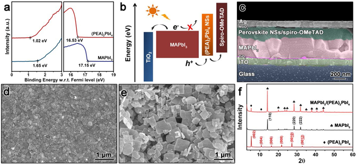
To determine the bandgap of the (PEA)2PbI4 NSs and MAPbI3, UV–vis absorption spectroscopy was employed, and the results are shown in Fig. S2 (Supporting information). The optical band gap (Eg) could be calculated from the Tauc's formula. The Eg of MAPbI3 and (PEA)2PbI4 NSs are 1.65 and 2.23 eV, respectively. Evidently, replacing MA+ with larger cations leads to an increasement of bandgap [32]. Meanwhile, ultra-violet photoemission spectra (UPS, Fig. 2a) was used to investigate the energy levels of these perovskites (i.e., MAPbI3 and 2D (PEA)2PbI4 NSs) [33, 34]. The valence band maximum (VBM) level values could be calculated from Fig. 2a. And the conduction band minimum (CBM) level values, calculated by using the equation CB = VB+energy gap, are 4.07 and 3.48 eV for MAPbI3 and (PEA)2PbI4 NSs, respectively. All above energy levels results are summarized in Table S1 (Supporting information). From the aspect of band alignment in PSCs, the synthesized 2D (PEA)2PbI4 NSs could be employed as the hole extraction layers in MAPbI3-based PSCs. The structure of fabricated device is ITO/TiO2/MAPbI3/2D (PEA)2PbI4 NSs/spiro-OMeTAD/MoO3/Ag (see Methods in the Supporting information). Meanwhile, the schematic energy level diagram of each materials in the 3D/2D devices is provided in Fig. 2b. From the analyses of energy levels for different components, the VBM of (PEA)2PbI4 NS is located between the VBM of MAPbI3 and the highest occupied molecular orbital (HOMO) of Spiro-MeOTAD, which could provide highly effective pathways for hole transport thus reduce the interfacial charge recombination loss.

|
Download:
|
| Fig. 2. (a) UPS spectra of MAPbI3 and (PEA)2PbI4 NS films on ITO glass as substrate. (b) Schematic energy level diagram of the 3D/2D MAPbI3/(PEA)2PbI4 PSCs. (c) Cross-sectional SEM image of a typical MAPbI3 PSC with incorporation of 2D (PEA)2PbI4 NSs. (d) Top-view SEM image of MAPbI3 film. (e) Top-view SEM image of 2D (PEA)2PbI4 NSs covered on the MAPbI3 film. (f) XRD patterns of the (PEA)2PbI4 NS, MAPbI3 and MAPbI3/(PEA)2PbI4 composite films, respectively. | |
The corresponding cross-section scanning electron microscope (SEM) image of PSCs was taken to demonstrate the structure of devices, as shown in the Fig. 2c. Different from the cross-section SEM image taken from the complete device, the top-down images were aimed to observe the uniformity and continuity of the (PEA)2PbI4 NSs on the 3D MAPbI3 layer. Figs. 2d and e show the morphology of the 3D MAPbI3 and 3D/2D MAPbI3/(PEA)2PbI4 films, respectively.
Apparently, the pristine 3D film was densely packed and composed of MAPbI3 crystals with grain-size around 200 nm. After spin-coating the synthesized (PEA) 2PbI4 NSs, the surface of MAPbI3 was fully covered with the (PEA)2PbI4 NSs. After fabricated the whole device, the changes in the morphology of (PEA)2PbI4 NSs based devices are negligible according to the cross-section SEM image due to the introduction of thicker spiro-OMeTAD layer. Meanwhile, the X-ray diffraction (XRD) measurement was carried out to prove the presence of (PEA)2PbI4 NSs on the surface of MAPbI3. Fig. 2f shows the composite films contain two sets of peaks, which could be indexed to the crystalline MAPbI3 and (PEA)2PbI4 NSs. After the deposition of (PEA)2PbI4 NSs, the main diffraction peaks associated with the (110), (220) and (222) plane from MAPbI3 show no changes. And a new set of diffraction peaks for 2D (PEA)2PbI4 NSs associated with the (002) and (004) planes appeared in the patterns of composites film. Moreover, Fig. S3 (Supporting information) presents the high resolution XPS spectra for the C, N, Pb and I elements in both MAPbI3 and MAPbI3/(PEA)2PbI4 composite film, respectively. The XPS spectra of the MAPbI3 and MAPbI3/(PEA)2PbI4 films show the same peak positions and comparable intensities. The binding energy for Pb 4f5/2 and Pb 4f7/2 are located at 142.7 eV and 137.9 eV, and the characteristic peaks for I 3d3/2 and I 3d5/2 are observed at 630.4 eV and 618.9 eV, respectively.
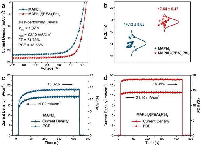
To investigate the function of (PEA)2PbI4 NSs layers in PSCs, the current density versus voltage (J-V) curves for the best PSC devices under AM 1.5G irradiation (100 MW/cm2) are shown in Fig. 3a. The MAPbI3 device as the reference device produced a PCE of 15.4%, with a VOC of 1.04 V, a JSC of 21.81 mA/cm2, and an FF of 67.89%. Upon the introduction of (PEA)2PbI4 NSs at the interface of MAPbI3 film and HTL layer (i.e., spiro-OMeTAD), the photovoltaic performance improved significantly. the 3D/2D MAPbI3/(PEA)2PbI4 device produced a VOC of 1.07 V, a JSC of 23.15 mA/cm2, and an FF of 74.78%, corresponding to a PCE of 18.53%. The significant improved JSC and FF as well as the slightly increased VOC play the key roles in the enhancement of PCE. To test the reproducibility, we fabricated twenty samples for each type of PSCs and evaluated their photovoltaic performance. Fig. 3b and Fig. S4 (Supporting information) show the statistics of detailed parameters for these two types of devices. The PCEs of MAPbI3/(PEA)2PbI4 devices were distributed in a relatively narrow range, indicated their excellent reproducibility. The average photovoltaic parameters could be found in the Table S2 (Supporting information). The average PCEs of MAPbI3 and MAPbI3/(PEA)2PbI4 PSCs obtained in our work were 14.12% ± 0.63% and 17.64% ± 0.47%, respectively. These results are consistent with that of the best parameters of two kinds of devices. And the performance is comparable to the best perovskite solar cells with 3D/perovskite nanomaterial heterostructures (Table S3 in Supporting information).

|
Download:
|
| Fig. 3. (a) J-V characteristics of the best performing devices based on MAPbI3 and MAPbI3/(PEA)2PbI4 perovskite films. (b) Statistics of the PCE distribution for the fabricated MAPbI3 and MAPbI3/(PEA)2PbI4 PSCs (20 devices). (c) Steady-state photocurrent density of MAPbI3 PSCs at the maximum power point (0.79 V). (d) Steady-state photocurrent density of MAPbI3/(PEA)2PbI4 PSCs at the maximum power point (0.87 V). | |
Photocurrent hysteresis is another important factor for the PSCs. In Fig. S5 and Table S4 (Supporting information), the MAPbI3 PSCs exhibited an obvious photocurrent hysteresis with PCEs of 15.40% and 7.58% under a reverse (from forward bias to short circuit) and forward scan (from short circuit to forward bias), respectively. Hence, the hysteresis factor could be quantified by using the following equation:
| $Hysterresis factor = (PCEreverse - PCEforward)/PCEreverse$ |
Compared with the high hysteresis factor from MAPbI3 PSCs (i.e., 50.8%), the MAPbI3/(PEA)2PbI4 PSCs exhibited a decreased hysteresis factor of 43.7%. The current peak could be observed from the forward bias region for the reverse scans, indicating a typical signal for a diode. These results clearly demonstrated it requires a longer time to reach to the stable operation [32]. According to the literature, the deteriorative degrade of hysteresis is strongly dependent on the device structure. At the same scan rate, the MAPbI3 device with the planar structure shows a more obvious hysteresis [35]. To further study the hysteresis, we also measured the steady-state photocurrent and PCE under the maximum power point over 400 s. According to the results from the Fig. 3c and Table S5 (Supporting information), the MAPbI3 PSCs show a stabile photocurrent of 19.02 mA/cm2 when the bias voltage is 0.79 V, and generate a PCE of 15.02% which is consistent with the PCE value calculated from the J-V measurements. In contrast, the PCE of MAPbI3/(PEA)2PbI4 PSCs rapidly reached to a stable value of 18.35% at bias voltage of 0.87 V, which is close to the best PCE value of 18.53% (Fig. 3d, Table S5). Compared to the MAPbI3 PSCs, both photocurrent and PCE of MAPbI3/(PEA)2PbI4 PSCs exhibited much faster response, which should be attributed to the less ionic migration, optimal graded interface, and/or synergistic of these two factors. Moreover, the faster stabilizing rate and higher stable PCE also demonstrated the less defects in the 3D/2D MAPbI3/(PEA)2PbI4 perovskite film, which is also help for the decrease of charge recombination and alleviation of hysteresis.
We also analysed the absorption and photoluminescence spectra of these two films (i.e., MAPbI3 and MAPbI3/(PEA)2PbI4) to get better understanding about the generation and recombination of electron-hole pairs. As shown in Fig. 4a, the strong absorption of these films is mainly come from the active layer, i.e., MAPbI3. Due to the thin thickness of the (PEA)2PbI4, there is a slight enhancement for the absorption of the (PEA)2PbI4 below 500 nm. Meanwhile, because of small amount of (PEA)2PbI4 NSs on the active layer, theoretically, the light absorption properties of (PEA)2PbI4 NSs cannot improve the light harvesting strongly. Therefore, the difference in PCE should be ascribed to the graded interface introduced by the (PEA)2PbI4 NSs on MAPbI3. To further investigate the interaction between the MAPbI3 and (PEA)2PbI4 NSs, photoluminescence measurements were employed. From the Fig. 4b, the emission of both samples is centered at 770 nm, which is attribute to exciton recombination and luminescence of MAPbI3. However, compared to the MAPbI3, the decreased photoluminescence intensity indicates a faster electron-hole separation followed by the hole extraction with the introduced (PEA)2PbI4 NSs on MAPbI3. According to the proposed mechanism from Fig. 2b, the photo generated holes in the MAPbI3 film could firstly transfer to the (PEA)2PbI4 NSs then to the HTM layer, which is propitious to the improvement of PCE of PSCs.

|
Download:
|
| Fig. 4. (a) UV–vis absorption spectrum of MAPbI3 and MAPbI3/(PEA)2PbI4 films. (b) Steady-state photoluminescence curves for MAPbI3 and MAPbI3/(PEA)2PbI4 films detected from the glass side in the wavelength range of 670-850 nm. Images of (c) original perovskite film and (d) perovskite film after exposing in an ambient environment at 30 ℃ and with 90%±5% relative humidity for 5 h. Left: MAPbI3 film, right: MAPbI3/(PEA)2PbI4 film. | |
Besides the improved photovoltaic efficiency, another major concern is the durability of PSCs for real application, especially under moisture conditions. To directly evaluate their moisture stability, we tested the stability of the MAPbI3 film (left image in Fig. 4c) and MAPbI3/(PEA)2PbI4 composite film (right image in Fig. 4c) without any encapsulation under the ambient conditions at 30 ℃ and with the relative humidity of 90% ± 5%. After 5 h, the pure MAPbI3 film degraded dramatically, as shown in left image in Fig. 4d. However, there were no obvious colour changes for MAPbI3/(PEA)2PbI4 composite film (right image in Fig. 4c), indicating the 2D (PEA)2PbI4 NSs could provide sufficient protection for MAPbI3 films from the high moisture environment.
We fabricated PSCs based on 3D/2D MAPbI3/(PEA)2PbI4 with dimensional graded heterojunction, which exhibited improved PCE and stability under moisture conditions. Comprehensive characterizations were carried out to investigate the effect of 2D (PEA)2PbI4 NSs on the performance of PSCs. It is demonstrated that the graded structure of MAPbI3/(PEA)2PbI4 could upshift the energy level, thus enhancing the hole extraction efficiency and decreasing the interface charge recombination. With the assistance of (PEA)2PbI4 NSs, the improved interfacial characteristics lead to an increasement in PCE with enhanced VOC, JSC and FF.
Declaration of competing interestThe authors report no declarations of interest.
AcknowledgmentsThe authors acknowledge the financial support of the National Natural Science Foundation of China (No. 61775011), and the Supplementary and Supportive Project for Teachers at Beijing Information Science and Technology University (2019-2021) (No. 5029011103).
Appendix A. Supplementary dataSupplementary material related to this article can be found, in the online version, at doi:https://doi.org/10.1016/j.cclet.2020.12.052.
| [1] |
Z. Wei, Y. Zhao, J. Jiang, et al., Chin. Chem. Lett. 31 (2020) 3055-3064. DOI:10.1016/j.cclet.2020.05.016 |
| [2] |
S.D. Stranks, G.E. Eperon, G. Grancini, et al., Science 342 (2013) 341-344. DOI:10.1126/science.1243982 |
| [3] |
G. Xing, N. Mathews, S. Sun, et al., Science 342 (2013) 344-347. DOI:10.1126/science.1243167 |
| [4] |
Q. Dong, Y. Fang, Y. Shao, et al., Science 347 (2015) 967-970. DOI:10.1126/science.aaa5760 |
| [5] |
T.M. Brenner, D.A. Egger, L. Kronik, et al., Nat. Rev. Mater. 1 (2016) 15007. DOI:10.1038/natrevmats.2015.7 |
| [6] |
X. Sun, D. Zhao, Z.a. Li, Chin. Chem. Lett. 29 (2018) 219-231. DOI:10.1016/j.cclet.2017.09.038 |
| [7] |
Y. Yang, N.D. Pham, D. Yao, et al., Chin. Chem. Lett. 29 (2018) 1242-1250. DOI:10.1016/j.cclet.2018.05.008 |
| [8] |
W.S. Yang, B.W. Park, E.H. Jung, et al., Science 356 (2017) 1376-1379. DOI:10.1126/science.aan2301 |
| [9] |
H. Zai, C. Zhu, H. Xie, et al., ACS Energy Lett. 3 (2018) 30-38. DOI:10.1021/acsenergylett.7b00925 |
| [10] |
Y. Rong, Y. Hu, A. Mei, et al., Science 361 (2018) eaat8235. DOI:10.1126/science.aat8235 |
| [11] |
T. Leijtens, K. Bush, R. Cheacharoen, et al., J. Mater. Chem. A 5 (2017) 11483-11500. DOI:10.1039/C7TA00434F |
| [12] |
J. Yan, W. Qiu, G. Wu, et al., J. Mater. Chem. A 6 (2018) 11063-11077. DOI:10.1039/C8TA02288G |
| [13] |
I.C. Smith, E.T. Hoke, D. Solis-Ibarra, et al., Angew. Chem. 126 (2014) 11414-11417. DOI:10.1002/ange.201406466 |
| [14] |
F. Xu, T. Zhang, G. Li, Y. Zhao, J. Mater. Chem. A 5 (2017) 11450-11461. DOI:10.1039/C7TA00042A |
| [15] |
S. Yang, W. Niu, A.L. Wang, et al., Angew. Chem. Int. Ed. 56 (2017) 4252-4255. DOI:10.1002/anie.201701134 |
| [16] |
S. Ahmad, X. Guo, Chin. Chem. Lett. 29 (2018) 657-663. DOI:10.1016/j.cclet.2017.08.057 |
| [17] |
J.W. Lee, Z. Dai, T.H. Han, et al., Nat. Commun. 9 (2018) 3021. DOI:10.1038/s41467-018-05454-4 |
| [18] |
Z. Wang, Q. Lin, F.P. Chmiel, et al., Nat. Energy 2 (2017) 17135. DOI:10.1038/nenergy.2017.135 |
| [19] |
D.S. Lee, J.S. Yun, J. Kim, et al., ACS Energy Lett. 3 (2018) 647-654. DOI:10.1021/acsenergylett.8b00121 |
| [20] |
C.M.M. Soe, W. Nie, C.C. Stoumpos, et al., Adv. Energy Mater. 8 (2018) 1700979. DOI:10.1002/aenm.201700979 |
| [21] |
B.E. Cohen, M. Wierzbowska, L. Etgar, Adv. Funct. Mater. 27 (2017) 1604733. DOI:10.1002/adfm.201604733 |
| [22] |
P. Chen, Y. Bai, S. Wang, et al., Adv. Funct. Mater. 28 (2018) 1706923. DOI:10.1002/adfm.201706923 |
| [23] |
Y. Bai, S. Xiao, C. Hu, et al., Adv. Energy Mater. 7 (2017) 1701038. DOI:10.1002/aenm.201701038 |
| [24] |
M. Tai, Y. Zhou, X. Yin, et al., J. Mater. Chem. A 7 (2019) 22675-22682. DOI:10.1039/c9ta08564e |
| [25] |
Q. Jiang, Y. Zhao, X. Zhang, et al., Nat. Photonics 13 (2019) 460-466. DOI:10.1038/s41566-019-0398-2 |
| [26] |
E.A. Alharbi, A.Y. Alyamani, D.J. Kubicki, et al., Nat. Commun. 10 (2019) 3008. DOI:10.1038/s41467-019-10985-5 |
| [27] |
X. Xu, Z. Li, L. Zhu, et al., J. Mater. Chem. A 7 (2019) 1341-1348. DOI:10.1039/c8ta06044d |
| [28] |
T. Zhang, M. Long, M. Qin, et al., Joule 2 (2018) 2706-2721. DOI:10.1016/j.joule.2018.09.022 |
| [29] |
G. Liu, H. Zheng, X. Xu, et al., J. Mater. Chem. A 6 (2018) 18067-18074. DOI:10.1039/c8ta04936j |
| [30] |
Y. Cho, A.M. Soufiani, J.S. Yun, et al., Adv. Energy Mater. 8 (2018) 1703392. DOI:10.1002/aenm.201703392 |
| [31] |
L. Zhu, H. Zhang, Q. Lu, et al., J. Mater. Chem. C 6 (2018) 3945-3950. DOI:10.1039/c8tc00289d |
| [32] |
C. Li, J. Wei, M. Sato, et al., ACS Appl. Mater. Interfaces 8 (2016) 11526-11531. DOI:10.1021/acsami.6b02692 |
| [33] |
L. Lv, Q. Lu, Y. Ning, et al., Chem. Mater. 27 (2015) 44-52. DOI:10.1021/cm5028833 |
| [34] |
H.Y. Zhang, R. Li, W.W. Liu, et al., Int. J. Miner. Metall. Mater. 26 (2019) 387-403. DOI:10.1007/s12613-019-1748-2 |
| [35] |
H.S. Kim, N.G. Park, J. Phys. Chem. Lett. 5 (2014) 2927-2934. DOI:10.1021/jz501392m |