 2021, Vol. 32


b Hubei Key Laboratory of Low Dimensional Optoelectronic Materials and Devices, Hubei University of Arts and Science, Xiangyang 441053, China;
c ARC Centre of Excellence for Electromaterials Science, Intelligent Polymer Research Institute, Australia Institute for Innovative Materials (AIIM), Innovation Campus, University of Wollongong, Wollongong 2519, Australia
Hydrogen production from solar water splitting, which offers a promising technology to solve the global challenge of the depletion of fossil fuels and the associated environmental pollution, has attracted significant interest over the past years [1-4]. Since the pioneering work of Fujishima and Honda in 1972 [5], numerous inorganic semiconductor materials, including metal oxides, metal sulfides, metal nitrides, and metal phosphides, have been explored for water photolysis [6-12]. Unfortunately, most reported inorganic photocatalysts exhibit intrinsic disadvantages such as wide band gap (>3.0 eV), ineffective utilization of solar energy (can only absorb ultraviolet light), and high electron-hole recombination rate induced by the low carrier mobility and long migration distance [13, 14]. Hence, their photocatalytic performances are still yet to achieve the requirement of practical application.
Compared to the bulk photocatalysts, two-dimensional (2D) photocatalysts possess unique atomic structures and unprecedented properties, thus have been hot topics of extensive experimental and theoretical researches [15-22]. For instance, Sun et al. [23] reported that the photocurrent density of single-layer SnS2 reached up to 2.75 mA/ cm2 at 1.0 V, which was 72 times larger than the bulk counterpart. Cheng et al. [24] found that the hydrogen generation rates of synthesized FePS3 sheets were 3 times higher than that of bulk FePS3. Qiao et al. [25] theoretically predicted that PdSeO3 monolayer can be easily exfoliated from the bulk phase, and its reduction/oxidation ability was high enough for splitting pure water into hydrogen and oxygen. Most recently, Yang's group designed a new 2D photocatalyst (F-BNBN-H) with large intrinsic dipole, in which the band gap restriction (1.23 eV) for direct overall water splitting can be broken and thus utilizing the near-infrared light would be achieved [26]. Referring to this novel model, some 2D materials with intrinsic electric polarization, such as Janus transition metal dichalcogenides monolayers [27-30], Sc2CO2 [31], M2XY (M=Ga, In; X/Y = S, Se, Te) [32-34] and M2X3 (M = Al, Ga, In; X = S, Se, Te) [35, 36], have been exploited as photocatalyts for water splitting. In virtue of the intrinsic electric field produced by the intrinsic dipole, these 2D materials have not only appropriate band gap and band edge alignments, but also very low recombination possibility of photongenerated carriers, making them be promising candidates as highly efficient photocatalysts. Nevertheless, the amount of such built-in dipoled 2D photocatalysts is still rather rare. It is still necessary to search for other 2D semiconductor materials with good structure stability, appropriate electronic properties, and large intrinsic dipoles simultaneously.
As allotropes of phosphorene, layered group-IV monochalcogenides have been theoretically predicted and experimentally synthesized recently, which show good promise for various applications in these aspects of gas sensors, solar cells, anode materials for ion batteries, and photocatalysts [37-40]. In particular, the monolayer materials in the buckled configuration, similar to blue phosphorene, usually generate the intrinsic dipoles due to by the large difference of electronegativity between the top and bottom sides. Monolayer silicon and germanium monochalcogenides (i.e., SiS, SiSe, GeS and GeSe) have been found to be suitable for overall photocatalytic water splitting [41-44]. Inspired by these, we thus wonder whether the monolayer carbon monochalcogenides (CX, X = S, Se) can steadily exist as free-standing sheets and whether they are high efficient photocatalysts for water splitting. Hence, we systematically investigate the structural, electronic, and photocatalytic properties of blue-phase CX (X = S, Se) monolayers by performing first-principles calculations.
First-principles calculations are carried out based on the density functional theory with the projector augmented wave method [45], as implemented in Vienna Ab initio Simulation Package (VASP) [46]. The Perdew-Burke-Ernzerhof (PBE) functional [47] is adopted for optimizing the geometric structure, and the Heyd-Scuseria-Ernzerhof (HSE06) functional [48, 49] is adopted for giving more accurate electronic and optical properties, in which the 25% PBE exchange part is replaced by the Hartree-Fock exact exchange in the short-range. Namely, the mixing parameter (α) of the HSE06 functional is set to be 0.25. The energy cutoff energy is set to 500 eV, and the Monkhorst-Pack mesh [50] of k-points 21 × 21 × 1 points are used to sample the Brillouin zone. A vacuum region of 20.0 Å along the z direction is applied to avoid the coupling effect of two adjacent image layers. The convergence criterias of total energy and atomic forces are set as 1 × 10⁻⁵ eV and 0.02 eV/Å, respectively. Dipole correction along the z direction is needed to cancel the errors of electrostatic potential, atomic force, and total energy, caused by periodic boundary condition.
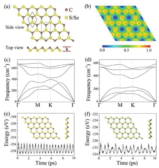
Akin to blue phosphorene, the CX monolayers have a buckled hexagonal structure with the C and S(Se) atoms interlocked and distributed alternately, as shown in Fig. 1a. After optimization, the lattice constant of monolayer CS is predicted to be 2.82 Å with a C–S bond length of 1.87 Å and buckling height of 0.92 Å, while for monolayer CSe, the lattice parameter, C–Se bond length and buckling height increase to 3.07 Å, 2.06 Å and 1.04 Å, respectively. The reason is that the atomic radius of Se atom is larger than that of S atom. To characterize the bonding features in these CX monolayers, the electron localization functions (ELF) are calculated and depicted in Fig. 1b and Fig. S1 (Supporting information), where the values of 1.0, 0.5 and 0.0 represent the fully localized electron, the free electron-gas and very low electron density, respectively. It can be seen that the ELF values around the C and S(Se) sites are different, and a substantial concentration of electrons are localized at the regions between C and S(Se) atoms, revealing the presence of polar covalent bonding in monolayer CS and CSe. The Bader charge analysis further illustrates that 0.23(0.39) electrons are transferred from S(Se) atom to C atom, also confirming the polar chemical bonding.

|
Download:
|
| Fig. 1. (a) Geometric structure of CX monolayers from thetop and side views. The hexagonal primitive cell and orthogonal supercell are marked by black and blue lines, respectively. (b) Visualization of the electron localization function for monolayer CS. Calculated phonon dispersions of monolayer (c) CS and (d) CSe. The total energy fluctuations during 10 ps AIMD simulations at room temperature (300 K) for monolayer (e) CS and (f) CSe. Insets in (e) and (f) show the final geometric structures after AIMD simulation. | |
Before moving on to other properties, we first focus on the structural stability of the CX monolayers, including their dynamical, thermal, and mechanical stability. To assess their dynamical stabilities, the phonon dispersion curves are calculated based on the frozen-phonon method as implemented in the PHONOPY package [51]. The 5 × 5 × 1 supercell and 4 × 4 × 1 Γ centered k-point sampling are used for the phonon calculations. As shown in Figs. 1c and d, we find that the low-frequency optical and acoustic modes separate apart from each other around the Γ point, and the frequencies of all phonon modes in the entire Brillouin zone are positive. The highest frequencies of monolayer CS and CSe reach up to 680 cm−1 and 580 cm−1, respectively, which are comparable to those of silicene (550 cm−1) [52] and blue phosephorene (520 cm−1) [53]. These results demonstrate that our proposed two monolayer materials are dynamically stable. Furthermore, we examine their thermal stability by performing ab initio molecular-dynamics (AIMD) simulations at 300 K using a 5 × 5 × 1 supercell. As plotted in Figs. 1e and f, the total energies have small fluctuations and the initial geometric structures are well maintained after 10 ps simulation with the NVT ensemble, suggesting that monolayer CS and CSe can be stable at the room-temperature. In addition, we also investigate the effect of the O2 molecule on their structural stabilities. As shown in Fig. S2 (Supporting information), we can see that the distances from the O2 molecule to the CS and CSe monolayers are 2.67 and 2.52 Å, respectively, and the corresponding binding energy (Ea) are 151 meV and 223 meV. This indicates that O2 molecule is bonded to the monolayers mainly by vdW force. As a result, our proposed CX monolayers can be stable in the presence of O2.
Additionally, we systematically examine the elastic properties of the CX monolayers to analyze the mechanical stability. Based on the strain-energy method, the calculated elastic constants of monolayer CS (CSe) are C11 = C22 = 132.64 (95.59) N/m, C12 = 14.69 (16.20) N/m and C66 = 58.97 (39.69) N/m. Clearly, the Born-Huang criteria of mechanical stability for 2D hexagonal materials (e.g., C11C22 - C122 > 0, C66 > 0) is nicely satisfied, reflecting the mechanical robustness of monolayer CS and CSe. Given these elastic constants, we also calculate the in-plane Young's modulus (Y) and Poisson's ratio (υ), which are defined as Y = (C112 - C122)/C11 and υ = C12/C11, respectively. The in-plane Young's modulus (Y) and Poisson's ratio (υ) of monolayer CS (CSe) are found to be 131.01 (92.84) N/m and 0.11 (0.17), respectively. These results are lower than graphene [54] but comparable to MoS2 [55], indicate that the bonding between atoms in these two monolayers are strong and would avail to avoid the curling.
Encouraged by the excellent stability of the CX monolayers, we then turn to discuss their electronic properties by computing the band structures as well as the density of states (DOSs). As shown in Fig. 2, both of CS and CSe monolayers present indirect band gap semiconductor characteristics. The valence band maximum (VBM) of CS monolayer lies at the point between K and Γ points and their conduction band minimum (CBM) is situated at the M point. As for CSe monolayer, the VBM is still located on the K → Γ path while the CBM is located between the Γ and M points. Although a direct gap semiconductor is preferred, the materials with indirect band gaps can also be used as promising photocatalysts for water splitting because they advantageously reduce the recombination possibility of photogenerated electron-hole pairs. On basis of the HSE06 calculation, the predicted band gap values are 2.41 eV for CS and 2.46 eV for CSe. Noted that these values are lower than the band gap of metal-free graphitic carbon nitride (g-C3N4), which has been experimentally identified as a visible-light-responsive photocatalyst [56, 57]. From the computed partial DOSs depicted in the Fig. 2, we can see that the VBMs of monolayer CS and CSe are mainly contributed by X 3p, C 2s and C 2p states, while their CBMs are primarily originated from the hybridization of X 3p and C 2p states.

|
Download:
|
| Fig. 2. HSE06 calculated electronic band structures and projected density of states of monolayer (a) CS and (b) CSe. Here, the Fermi energy levels are scaled to zero and shown as red dashed lines. | |
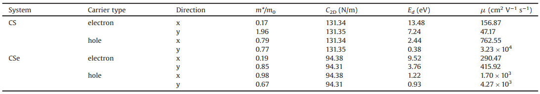
To further explore the charge transport properties for potential energy conversion application, the carrier mobility of CX monolayers are estimated according to the deformation potential (DP) theory proposed by Bardeen and Shockley [58, 59]. The carrier mobility for 2D materials is described as
|
(1) |
where e, 

|
|
Table 1 Carrier effective mass (m*), 2D elastic modulus (C2D), deformation potential (Ed), and carrier mobility (μ) of CX monolayers. |
Now, we explore the possibility of using CX monolayers as photocatalysts for water splitting. Owing to the electronegativity difference between C and X atoms, the C atoms in the top layer are negatively charged whereas the X atoms in the bottom layer are positively charged. Thus, an intrinsic dipole (P) is generated, which are found to be 0.43 D for CS and 0.51 D for CSe. As we known, these relatively large dipole can introduce internal electric field (Eeff) in monolayer CX, which are along with the perpendicular plane direction and point from X side to C side. Moreover, as described by the Yang group, the energy levels of the monolayer CS and CSe would bend along the direction of the built-in Eeff, accompanied by the presence of the difference (ΔΦ) between the vacuum energy levels on the two respective sides [26]. As shown in Figs. 3a and b, the top and bottom vacuum regions are different by 2.34 and 2.38 eV for monolayer CS and CSe, respectively, which are as large as some widely known 2D materials with intrinsic electric polarization [27-36], such as MXene, germanium monochalcogenide and Janus metal chalcogenides.

|
Download:
|
| Fig. 3. Electrostatic potentials of monolayer (a) CS and (b) CSe. Band alignments with respect to the redox potentials of water for monolayer (c) CS and (d) CSe. Eeff represents the internal effective electric field generated by the intrinsic dipole. | |
To assess whether monolayer CX possess strong reduction/oxidation ability, we further calculate their accurate VBM/CBM locations by considering the vacuum level corrections, and then align them relative to the redox potential levels for H+/H2 (−4.44 eV at pH 0) and O2/H2O (−5.67 at pH 0), which are illustrated in Figs. 3c and d. It should be pointed that the photogenerated electrons and holes can aggregate separately on disparate sides of monolayer CX because of the built-in electric field, meaning that the hydrogen reduction reaction and water oxidation reaction happen on the X and C sides, respectively. On the X atomic layer side, the CBM potentials of CX monolayers (−3.47 eV for CS and −3.12 eV for CSe) lie above hydrogen reduction potential, showing that H+ can be reduced to H2 by the photogenerated electrons. On the C atomic layer side, the VBMs (−8.21 eV for CS and −7.96 eV for CSe) lie below water oxidation potential, showing that H2O can be oxidized to O2 by the photogenerated holes. Following a previous study, the energy difference between the CBM and the hydrogen reduction potential is defined as the potential of photogenerated electrons for hydrogen evolution reaction (Ue), while the energy difference between the VBM and the water oxidation potential is calculated as the potential of photogenerated holes for oxygen evolution reaction (Uh). Hence, the Ue and Uh are calculated to be 0.97/2.54 eV for CS and 1.32/2.29 eV for CSe, suggesting that both of them are capable to work as highly efficient photocatalysts for water splitting without using sacrificial reagents or cocatalysts.
In practical applications for energy storage and conversion, the external strain would inevitably occur and usually play an important role in modulating the properties of 2D photocatalyst materials. As such, we further study the effects of in-plane biaxial strains in the range from −5% to 5% on the electronic structures and photocatalytic properties of monolayer CS and CSe. The biaxial strain is defined as 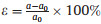

|
Download:
|
| Fig. 4. Band structures of monolayer (a) CS and (b) CSe at −5%, −3%, −1%, 1%, 3% and 5% biaxial strain. The Fermi levels (red dashed lines) are set to zero. | |
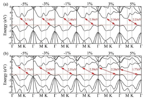
Meanwhile, the dipole moment P and electrostatic potential difference of monolayer CS and CSe are expected to be effectively modulated by applying external biaxial strain. To explore this issue, the variations of the dipole moment and electrostatic potential difference as a function of the biaxial strain are studied. As shown in Fig. 5a, the dipole moment of monolayer CS/CSe slightly decrease with the biaxial strain changing from −5% to 5%, for example, 0.46/0.54 D, 0.45/0.53 D, 0.41/0.50 D and 0.39/0.49 D at −5%, −3%, 3% and 5% strain. The applied strain has similar influences on the electrostatic potential difference of monolayer CX, which can be engineered from 2.48/2.54 eV to 2.12/2.16 eV for the CS and CSe monolayers, respectively. These values under the compressive and tensile strain states are still sufficiently large to induce strong intrinsic electric field, and thus remarkable charge separation can also occur in these strained CX systems.

|
Download:
|
| Fig. 5. Strain effects on (a) electrostatic potential differences and dipole moments, (b) band edge positions of monolayer CS and CSe. | |
To explore the strain effect on the reduction/oxidation ability of monolayer CS and CSe, their band edge alignments as a function of the biaxial strain are further calculated and shown in Fig. 5b. It should be noted that the redox potentials of water splitting depend on the pH value of the solution, which increase with pH by pH × 0.059 eV [63]. Thus, the band edge alignments of the CS and CSe monolayers as well as the reduction/oxidation ability will change in different solution environments. Consequently, the water redox potential at the acidic (pH 0) and neutral environment (pH 7) are computed and plotted in Fig. 5b by light gray and green horizontal dashed lines, respectively. We can see that applying compressive strain makes the Ue and Uh distinctly increase, while they gradually decrease when introducing external tensile strain. More fascinatingly, the CBM energies of all strained monolayer CX systems are higher than the reduction potential of H+/H2 and the corresponding VBM energies are lower than the oxidation potential of O2/H2O. The band edge positions are all situated at the favorable positions regardless of acidic or neutral environment, satisfying the requirements of photocatalyst for overall water splitting.
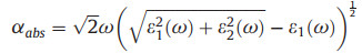
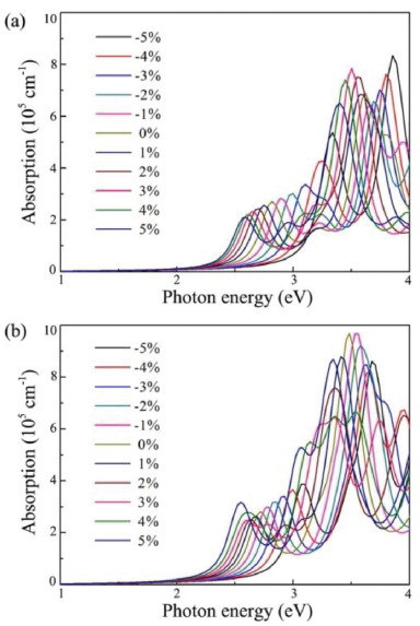
It is well-known that the light-harvesting performance is also an essential ingredient in determining the photocatalytic efficiency of water splitting. So that, we finally simulate the optical absorption spectrums of monolayer CX systems based on the HSE06 functional. According to the frequency-dependent dielectric function 
|
(2) |
where ε1(ω) and ε2(ω) are the real and imaginary parts of dielectric function, respectively. Fig. 6 shows the obtained results for monolayer CS and CSe within the strain range of −5%~5%. Here, only the absorption spectrums that the polarization directions are parallel to the planes of monolayer CX are considered. For the CS and CSe monolayers at strain-free states, the optical absorptions can be activated by the incoming light irradiation with photon energies higher than about 2.40 eV, which are coincident with the values of the band gaps obtained in pervious calculations. Moreover, they exhibit strong light absorption in both the ultraviolet and visible-light region, and the absorption intensities are as large as about 105 cm−1. As for monolayer CX systems under compressive strains, blue-shifted absorption edges in their absorption spectrums are observed, which are due to their larger band gaps. However, when the biaxial tensile strains are applied at monolayer CS and CSe, the absorption curves are considerably extended toward the visible-light region because of the narrowing of band gaps. These above results indicate that our proposed CX monolayers have outstanding absorption behaviours and can absorb as much visible-light as possible by tensile strain engineering, suggesting that they are promising metal-free photocatalyst for visible-light-driven water splitting.

|
Download:
|
| Fig. 6. Optical absorption spectrums of monolayer (a) CS and (b) CSe within the strain range of −5% to 5%. | |
For the practical application of photocatalytic water splitting, of course require the semiconductor material to be hydrophilic, which is another significant parameter characterizing its performance. To investigate how strong the interactions are between the H2O molecule and our proposed CX monolayers, several possible adsorption configurations are considered and geometrically optimized. The most energetically favorable configurations for H2O molecule adsorbed on CX monolayers are shown in Fig. S5 (Supporting information). The distances from the H2O molecule to the CS and CSe monolayers are 2.29 and 2.09 Å, respectively, and the corresponding binding energy (Ea) are 191 meV and 235 meV. The relatively large Ea suggests a strong interaction between the H2O molecule and the monolayers, ensuring better photocatalytic water-splitting activity.
In conclusion, by performing first-principles calculations, we systematically investigate the structural, electronic and photocatalytic properties of blue-phase CX (X = S, Se) monolayers. From the calculated phonon spectrums and elastic constants as well as AIMD simulations, we first verify that the proposed CX monolayers are dynamically, thermally, and mechanical stable. Then, CS and CSe monolayers are found to be indirect semiconductors with band gap of 2.41 and 2.46 eV, respectively. The calculated hole mobility along the b direction can be as high 3.23 × 104 cm2 V−1 s−1 for CS and 4.27 × 103 cm2 V−1 s−1 for CSe, which are comparable to those of many recently reported 2D photocatalysts. Furthermore, internal electrical fields are induced in these predicted monolayer materials due to the large intrinsic dipole, reducing the possibility of electron-hole recombination. More fascinatingly, CS and CSe monolayers not only possess favorable band edge positions with respect to water redox potentials and but also have strong capacity of optical absorption with the intensity up to 105 cm-1. Finally, we find that applying external strain can further adjust the band gaps, band alignments, and optical absorption behaviours of CX monolayers. These theoretical findings suggest that our proposed CS and CSe monolayers have great potential in the field of photocatalytic water splitting.
Declaration of competing interestThe authors declare that they have no known competing financial interests or personal relationships that could have appeared to influence the work reported in this paper.
AcknowledgmentsThis work was partially supported by the National Natural Science Foundation of China (No. 21503149), by the Program for Innovative Research Team in University of Tianjin (No. TD13-5074), by the Project of Hubei University of Arts and Science (Nos. xk2020043, xk2020044, 2020kypyfy015).
Appendix A. Supplementary dataSupplementarymaterial related to this article canbefound, in the online version, at doi:https://doi.org/10.1016/j.cclet.2020.09.056.
| [1] |
Q. Wang, K. Domen, Chem. Rev. 120 (2020) 919-985. DOI:10.1021/acs.chemrev.9b00201 |
| [2] |
C. Dong, J. Ji, Z. Yang, et al., Chin. Chem. Lett. 30 (2019) 853-862. DOI:10.1016/j.cclet.2019.03.020 |
| [3] |
J. Wang, J. Huang, J. Meng, et al., RSC Adv. 7 (2017) 39877-39884. DOI:10.1039/C7RA03175K |
| [4] |
M. Zeng, L. Zhang, D. Wu, et al., Chin. Chem. Lett. 30 (2019) 1329-1334. DOI:10.1016/j.cclet.2019.01.026 |
| [5] |
A. Fujishima, K. Honda, Nature 238 (1972) 37-38. DOI:10.1038/238037a0 |
| [6] |
Y. Yang, S. Niu, D. Han, et al., Adv. Energy Mater. 7 (2017) 1700555. DOI:10.1002/aenm.201700555 |
| [7] |
J. Huang, R. Xie, Y. Hu, et al., Chem. Phys. Lett. 758 (2020) 137925. DOI:10.1016/j.cplett.2020.137925 |
| [8] |
J. Wang, J. Teng, L. Pu, et al., Int. J. Quantum Chem. 119 (2019) e25930. DOI:10.1002/qua.25930 |
| [9] |
Z. Wang, C. Li, K. Domen, Chem. Soc. Rev. 48 (2019) 2109-2125. DOI:10.1039/C8CS00542G |
| [10] |
L. Cheng, Q. Xiang, Y. Liao, et al., Energy Environ. Sci. 11 (2018) 1362-1391. DOI:10.1039/C7EE03640J |
| [11] |
Y. Sun, T. Zhang, C. Li, et al., J. Mater. Chem. A: Mater. Energy Sustain. 8 (2020) 13415-13436. DOI:10.1039/D0TA05038E |
| [12] |
Y. Yang, Y. Tang, H. Jiang, et al., Chin. Chem. Lett. 30 (2019) 2089-2109. DOI:10.1016/j.cclet.2019.10.041 |
| [13] |
C.-F. Fu, X. Wu, J. Yang, Adv. Mater. 30 (2018) 1802106. DOI:10.1002/adma.201802106 |
| [14] |
X. Zhou, H. Dong, ChemCatChem 11 (2019) 3688-3715. DOI:10.1002/cctc.201900567 |
| [15] |
J. Wang, M. Zhang, J. Meng, et al., RSC Adv. 7 (2017) 24446-24452. DOI:10.1039/C7RA01723E |
| [16] |
Y. Zhao, S. Zhang, R. Shi, et al., Mater. Today 34 (2020) 78-91. DOI:10.1016/j.mattod.2019.10.022 |
| [17] |
L. Zhao, Y. Li, G. Zhou, et al., Chin. Chem. Lett. 32 (2021) 900-905. DOI:10.1016/j.cclet.2020.07.016 |
| [18] |
J. Wang, X. Yang, J. Cao, et al., Comput. Mater. Sci. 150 (2018) 432-438. DOI:10.1016/j.commatsci.2018.04.049 |
| [19] |
F. Yu, L. Wang, Q. Xing, et al., Chin. Chem. Lett. 31 (2020) 1648-1653. DOI:10.1016/j.cclet.2019.08.020 |
| [20] |
S. Zhao, R. Nivetha, Y. Qiu, et al., Chin. Chem. Lett. 31 (2020) 947-952. DOI:10.1016/j.cclet.2019.11.045 |
| [21] |
Y. Wan, L. Wang, H. Xu, et al., J. Am. Chem. Soc. 142 (2020) 4508-4516. DOI:10.1021/jacs.0c00564 |
| [22] |
Y. Yang, M. Wu, X. Zhu, et al., Chin. Chem. Lett. 30 (2019) 2065-2088. DOI:10.1016/j.cclet.2019.11.001 |
| [23] |
Y. Sun, H. Cheng, S. Gao, et al., Angew. Chem. Int. Ed. 51 (2012) 8727-8731. DOI:10.1002/anie.201204675 |
| [24] |
Z. Cheng, T.A. Shifa, F. Wang, et al., Adv. Mater. 30 (2018) 1707433. DOI:10.1002/adma.201707433 |
| [25] |
M. Qiao, J. Liu, Y. Wang, et al., J. Am. Chem. Soc. 140 (2018) 12256-12262. DOI:10.1021/jacs.8b07855 |
| [26] |
X. Li, Z. Li, J. Yang, Phys. Rev. Lett. 112 (2014) 018301. DOI:10.1103/PhysRevLett.112.018301 |
| [27] |
Y. Ji, M. Yang, H. Lin, et al., J. Phys. Chem. C 122 (2018) 3123-3129. DOI:10.1021/acs.jpcc.7b11584 |
| [28] |
R. Peng, Y. Ma, B. Huang, et al., J. Mater. Chem. A: Mater. Energy Sustain. 7 (2019) 603-610. DOI:10.1039/C8TA09177C |
| [29] |
C. Xia, W. Xiong, J. Du, et al., Phys. Rev. B 98 (2018) 165424. DOI:10.1103/PhysRevB.98.165424 |
| [30] |
W. Chen, X. Hou, X. Shi, et al., ACS Appl. Mater. Interfaces 10 (2018) 35289-35295. DOI:10.1021/acsami.8b13248 |
| [31] |
C.F. Fu, X. Li, Q. Luo, et al., J. Mater. Chem. A Mater. Energy Sustain. 5 (2017) 24972-24980. DOI:10.1039/C7TA08812D |
| [32] |
A. Huang, W. Shi, Z. Wang, J. Phys. Chem. C 123 (2019) 11388-11396. DOI:10.1021/acs.jpcc.8b12450 |
| [33] |
R. da Silva, R. Barbosa, R.R. Mancano, et al., ACS Appl. Nano Mater. 2 (2019) 890-897. DOI:10.1021/acsanm.8b02135 |
| [34] |
Z. Wang, G. Zhou, J. Phys. Chem. C 124 (2020) 167-174. DOI:10.1021/acs.jpcc.9b09914 |
| [35] |
C.F. Fu, J. Sun, Q. Luo, et al., Nano Lett. 18 (2018) 6312-6317. DOI:10.1021/acs.nanolett.8b02561 |
| [36] |
P. Zhao, Y. Ma, X. Lv, et al., Nano Energy 51 (2018) 533-538. DOI:10.1016/j.nanoen.2018.07.010 |
| [37] |
C. Chowdhury, S. Karmakar, A. Datta, J. Phys. Chem. C 121 (2017) 7615-7624. DOI:10.1021/acs.jpcc.6b12080 |
| [38] |
J.R. Brent, D.J. Lewis, T. Lorenz, et al., J. Am. Chem. Soc. 137 (2015) 12689-12696. DOI:10.1021/jacs.5b08236 |
| [39] |
J. Wang, S. Li, F. Yun, et al., Int. J. Quantum Chem. 120 (2020) e26230. |
| [40] |
Z. Zhu, J. Guan, D. Liu, et al., ACS Nano 9 (2015) 8284-8290. DOI:10.1021/acsnano.5b02742 |
| [41] |
Y. Ji, M. Yang, H. Dong, et al., Nanoscale 9 (2017) 8608-8615. DOI:10.1039/C7NR00688H |
| [42] |
Y.L. Zhu, J.H. Yuan, Y.Q. Song, et al., J. Mater. Sci. 54 (2019) 11485-11496. DOI:10.1007/s10853-019-03699-y |
| [43] |
L. Sun, Y. Cui, L. Peng, et al., J. Catal. 373 (2019) 67-74. DOI:10.1016/j.jcat.2019.03.031 |
| [44] |
D. Gu, X. Tao, H. Chen, et al., Nanoscale 11 (2019) 2335-2342. DOI:10.1039/C8NR08908F |
| [45] |
P.E. Blöchl, Phys. Rev. B 50 (1994) 17953. DOI:10.1103/PhysRevB.50.17953 |
| [46] |
G. Kresse, J. Furthmüller, Phys. Rev. B 54 (1996) 11169. DOI:10.1103/PhysRevB.54.11169 |
| [47] |
J.P. Perdew, K. Burke, M. Ernzerhof, Phys. Rev. Lett. 77 (1996) 3865. DOI:10.1103/PhysRevLett.77.3865 |
| [48] |
J. Heyd, G.E. Scuseria, M. Ernzerhof, J. Chem. Phys. 118 (2003) 8207-8215. DOI:10.1063/1.1564060 |
| [49] |
J. Heyd, G.E. Scuseria, M. Ernzerhof, J. Chem. Phys. 124 (2006) 219906. DOI:10.1063/1.2204597 |
| [50] |
H.J. Monkhorst, J.D. Pack, Phys. Rev. B 13 (1976) 5188. DOI:10.1103/PhysRevB.13.5188 |
| [51] |
A. Togo, I. Tanaka, Scr. Mater. 108 (2015) 1-5. DOI:10.1016/j.scriptamat.2015.07.021 |
| [52] |
X.J. Ge, K.L. Yao, J.T. Lü, Phys. Rev. B 94 (2016) 165433. DOI:10.1103/PhysRevB.94.165433 |
| [53] |
Z. Zhu, D. Tománek, Phys. Rev. Lett. 112 (2014) 176802. DOI:10.1103/PhysRevLett.112.176802 |
| [54] |
R.C. Andrew, R.E. Mapasha, A.M. Ukpong, et al., Phys. Rev. B 85 (2012) 125428. DOI:10.1103/PhysRevB.85.125428 |
| [55] |
R.C. Cooper, C. Lee, C.A. Marianetti, et al., Phys. Rev. B 87 (2013) 035423. DOI:10.1103/PhysRevB.87.035423 |
| [56] |
J. Wang, Z. Guan, J. Huang, et al., J. Mater. Chem. A: Mater. Energy Sustain. 2 (2014) 7960-7966. DOI:10.1039/C4TA00275J |
| [57] |
J. Wang, X. Li, Y. You, et al., Nanotechnology 29 (2018) 365401. DOI:10.1088/1361-6528/aace20 |
| [58] |
J. Bardeen, W. Shockley, Phys. Rev. 80 (1950) 72-80. DOI:10.1103/PhysRev.80.72 |
| [59] |
J. Qiao, X. Kong, Z.X. Hu, et al., Nat. Commun. 5 (2014) 4475. DOI:10.1038/ncomms5475 |
| [60] |
Y. Cai, G. Zhang, Y.-W. Zhang, J. Am. Chem. Soc. 136 (2014) 6269-6275. DOI:10.1021/ja4109787 |
| [61] |
J. Xiao, M. Long, X. Zhang, et al., Sci. Rep. 5 (2015) 9961. DOI:10.1038/srep09961 |
| [62] |
X. Zhang, X. Zhao, D. Wu, et al., Adv. Sci. 3 (2016) 1600062. DOI:10.1002/advs.201600062 |
| [63] |
J. Wang, J. Meng, Q. Li, et al., Phys. Chem. Chem. Phys. 18 (2016) 17029-17036. DOI:10.1039/C6CP01001F |
| [64] |
M. Gajdoš, K. Hummer, G. Kresse, et al., Phys. Rev. B 73 (2006) 45112-45120. DOI:10.1103/PhysRevB.73.045112 |