 2021, Vol. 32


b Institute of Organic Optoelectronics, Jiangsu Industrial Technology Research Institute (JITRI), Suzhou 215211, China
Intramolecular charge-transfer (ICT) interaction is a fundamental property of π-systems end-capped with electron donor (D) and acceptor (A), which are usually connected via a π-conjugated spacer (D–π–A). The variation of the donor and acceptor is an effective approach for tuning the frontier orbitals to develop numerous conjugative push-pull materials which have widespread applications across various branches of optoelectronics [1-3]. Among them, the thermally activated delayed fluorescence (TADF) emitters have attracted considerable attention as the third-generation organic light-emitting diodes (OLEDs) materials because of their high electroluminescent (EL) efficiency and the absence of rare metals such as iridium (Ir) and platinum (Pt) [4-9]. Their molecular design greatly depends on the D–π–A type structure, in this way, the highest occupied and lowest unoccupied molecular orbitals (HOMOs and LUMOs) can be decoupled and the exchange integral between them can be minimized [10-12]. Resultantly, a sufficiently small singlet–triplet energy gap (ΔEST) can be achievable to make the materials harvest the singlet and the up-converted triplet excitons for radiation process with 100% internal quantum efficiency (IQE) [13, 14].
After years of efforts, now the D–π–A type emitters are successful in achieving high external quantum efficiency (EQE) for OLEDs [15-17]. Despite prosperous development on D–π–ATADF molecules, the infrastructural studies on other charge transfer (CT) emissive paradigms, such as D/A exciplex or unconjugated D/A molecules with D–σ–A connection, never stop. Recently, many groups started to explore unconjugated D/A interplay through space and have reported several TADF models based on spiro series, triptycene, xanthene, [2, 2] paracyclophane and polyethylene, etc. [18-22]. Unlike conjugated D–π–A system, the HOMO and LUMO wavefunctions are thoroughly separated at the ground state because of unconjugated D/A system. Nevertheless, due to the obviously low efficiency and unclear construction principle, the unconjugated D/A TADF material is currently in its infancy which needs further development both in material and theory.
In this communication, we reported a new TADF emitter, DM-Me-B, which has divided D/A conjugation and close D/A distance in space. The spiro-scaffold can rigidify the donor and impose the acceptor at the C1 site of fluorene to adopt face-to-face manner between D/A blocks (Fig. 1a). Therefore, CT process directly through space could facilely occur in this molecular structure. As a result, the DM-Me-B exhibited a suitable ΔEST of 0.25eV and high photoluminescence quantum yield (PLQY) due to the suppression of rotation from D/A groups. The devices have achieved high efficiency with nearly 20% EQE, which shows the potential of such structure in constructing high-performance TADF materials.

|
Download:
|
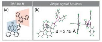
| Fig. 1. (a) Molecular structure and (b) single-crystal structure of emitter DM-Me-B. | |
The material was synthesized in three steps, which are shown in Scheme S1 (Supporting information). Firstly, Suzuki-Miyaura reaction was carried out between 9-fluorenone-1-boronic acid and 2-(4′-bromophenyl)-4, 6-diphenyl-1, 3, 5-triazine with proper catalyst/base of in THF/H2O solution. As the intermediate product has very poor solubility whereas the impurity has good solubility, the intermediate can be used directly without careful purification. The subsequent nucleophilic addition reaction took place at −78 ℃, and Friedel-Crafts cyclization followed to give the final product. The1H NMR, 13C NMR, mass spectrometry (Figs. S7-S9 in Supporting information) and elementary analysis were applied to characterize the chemical structures of the intermediate and DM-Me-B.
Single-crystal X-ray diffraction (XRD) was performed to further confirm the feasibility of the molecular design strategy as mentioned above (Fig. 1b). Notably, the D/A spatial distance measured from atom-to-centroid distance is only 3.15 Å, about 0.2 Å shorter than the interlayer distance of graphite [23], thus D/A intramolecular interaction could occur as charge transfer. Meanwhile, two packing modes are found in the single-crystal unit cell as that in Fig. S1 (Supporting information). One of the single-crystal packing modes of DM-Me-B illustrates the π-π stacking between triazine units with a plane-plane distance of 3.45 Å.
To clearly comprehend the geometrical and photophysical properties of the new emitter, we performed quantum-chemical calculations using density functional theory (DFT). Ground-state and excited-state geometries were optimized at the B3LYP [24]-D3BJ [25]/def2-SVP [26] and wb97xd [27]/def2-SVP [26] levels, respectively. As expected in Fig. 2a, HOMO wavefunction is located on the donor unit, whereas LUMO wavefunction is concentrated on the acceptor moiety, 2, 4, 6-triphenyl-1, 3, 5-triazine (TPZ), there is almost no distribution at the fluorene platform. In addition, hole-electron analysis was performed to illustrate the electron transition as Fig. 2b. For S1 state, the electrons transfer from the donor to acceptor, which demonstrates the CT state for S1. As for T1 state, the electron transition occurs between the acceptors, demonstrating the locally excited (LE) state for T1, which indicates a large spin-orbital coupling (SOC) constant and a large reverse intersystem crossing (RISC) rate. Furthermore, reduced density gradient (RDG) is calculated using Multiwfn [27] and then visualized in Fig. 2c and its scatter plot in Fig. 2d, which demonstrates the obvious intramolecular through-space attractive interactions (green region) and steric hindrance (brown region) between donor and acceptor moieties. The interaction can effectively restrict intramolecular vibrations and decrease energy loss of excited states.

|
Download:
|
| Fig. 2. (a) The distribution of HOMO and LUMO; (b) Hole-electron analysis for S1 and T1; (c) Reduced density gradient (RDG) using Multiwfn, the isovalue is 0.5; (d) RDG scatter plot. | |
The absorption spectrum was measured in dichloromethane (10−5 mol/L) at room temperature as Fig. 3a shows. Besides the π-π* transition around 280nm, DM-Me-B with unconjugated linker also displays an observable ICT transition band around 385nm. It is worth noting that such kind of ICT absorption band is characteristic in mostly D–π–A type TADF materials, but rare in reported D–σ–A type ones [28], indicating the mixing of the electronic wavefunctions in ground states between D/A units. This special feature could be attributable to the orbital overlap for efficient electron hopping within such a short cofacial distance in DM-Me-B. The fluorescence and phosphorescence spectra were measured in toluene at low temperature (77K), and the corresponding S1 and T1 energy levels were estimated from the onset of them as 3.10eV and 2.85eV, respectively (Fig. S2 in Supporting information). Thus, the experimental ΔEST for DM-Me-B is 0.25eV. When the solvent goes from n-hexane to dichloromethane, the emission peak of DM-Me-B presents significant bathochromic-shift, corresponding to its spatial CT nature (Fig. S3 in Supporting information).

|
Download:
|
| Fig. 3. (a) Normalized absorption (room temperature, 1×10⁻⁵ mol/L in DCM) and fluorescence and phosphorescence emission spectra (77 K, 1×10⁻⁵ mol/L in toluene) of DM-Me-B; (b) Time-dependent transient photoluminescence of DM-Me-B (30 wt%) in DPEPO blending film. | |
From Fig. 3b, the delay component of DM-Me-B can be clearly observed with microsecond-scale τTADF of 3.13 μs, which is much faster than the reported D–σ–A type TADF materials via unconjugated linker connection [29]. All photophysical data of DM-Me-B are summarized in Table S1 (Supporting information).
Before fabricating the OLED devices, several factors should be confirmed. The PLQYs are evaluated in toluene and blending film hosted by bis[2-(diphenylphosphino)phenyl]ether oxide (DPEPO). In toluene solution, the corresponding PLQY is 56%. Then, the PLQY value increases up to 73% in the blending film (30wt% in DPEPO), owing to the reducing collision-induced intramolecular non-radiative transition in a rigid matrix. The electrochemical properties were measured by cyclic voltammetry (CV). The curves of DM-Me-B present characteristics of reversible oxidation behaviors as Fig. S4 (Supporting information) shows. The HOMO energy levels (-5.29 eV) can be calculated from the onset of the first oxidation wave and the LUMO levels are determined to be -2.88eV. And the thermal properties of DM-Me-B are determined by thermogravimetric analysis (TGA) as Fig. S5 (Supporting information) shows. The decomposition temperature (Td) with 5% weight loss in the TGA curve is found at 401 ℃ under N2 atmosphere, suggesting the good thermal stability during vacuum deposition in the fabrication of OLED devices. Collectively, DM-Me-B could act as an effective TADF emitter with small ΔEST and high PLQY, as well as suitable energy levels for hole/electron injection (Table S1).
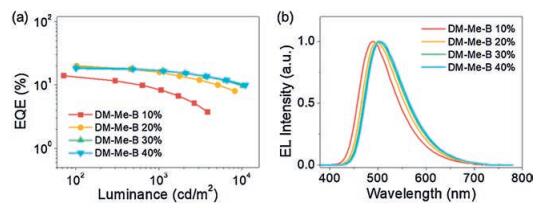
On the basis of the above properties, OLED devices are designed as ITO/ 1, 4, 5, 8, 9, 11-hexaazatriphenylenehexacarbonitrile (HAT-CN) (10nm)/1, 1-bis[(di-4-tolylamino)phenyl]cyclohexane (TAPC) (40nm)/4, 4', 4"-tris-(carbazol-9-yl)-triphenylamine (TCTA) (8nm)/1, 3-di(9H-carbazol-9-yl)benzene (mCP) (8nm)/DPEPO: emitters (20nm)/DPEPO (10nm)/1, 3, 5-tri[(3-pyridyl)-phen-3-yl]benzene (TmPyPB) (40nm)/8-hydroxyquinolinolato-lithium (Liq) (2nm)/Al (100nm), where HAT-CN is employed as the hole-injection layer, TAPC is used as hole-transporting layer, TCTA and mCP bilayers with relatively high triplet energy levels (T1) are embedded between TAPC and emitting layer. Besides of electron and exciton blocking capability, herein, they are also beneficial for the carrier injection to emitting layer due to the intermediate HOMO levels between TAPC and DPEPO matrix, such cascade HOMO levels could effectively reduce the driving voltage, as well as the energy loss during the carrier injection and transporting process owing to the large energy level gap. Following the emitting layer, 10nm thickness DPEPO neat film is used to confine the generated excitons within the light-emitting layer, then, TmPyPB and Liq are served as electron-transporting and electron-injection layers, respectively. The electrical properties of OLED devices, such as the current density to driving voltage (J-V) are presented in Fig. S6, it is noticeable that the driving voltage of OLEDs is decreased while increasing the doping ratios. For EL characteristics, as the doping ratio increased from 10wt% to 40wt%, the corresponding Commission Internationale de L'Eclairage (CIE) coordinates realize red-shift from greenish blue (0.21, 0.39) to green emission (0.27, 0.50), which might be ascribed to the enhanced intermolecular interaction when increasing the doping ratios of polar TADF emitters. Among them, the device with 30wt% doping ratio (D3) exhibits bluish-green emission, with a wavelength peak located at 500nm, and the corresponding CIE coordinates are (0.26, 0.48) (Fig. 4a). Furthermore, high EQE of 19.2% can be obtained, with slight efficiency roll-off (EQE=16.8%) under high luminance of 1000cd/m2, which is comparable to the device performance based on D–π–A type TADF emitters (Fig. 4b). All device data are summarized in Table S2.

|
Download:
|
| Fig. 4. (a) External quantum efficiency (EQEs) to luminance curves of DM-Me-B; (b) Electroluminescence (EL) spectra of OLED devices with different doping ratios based on DM-Me-B. | |
In conclusion, we construct a D/A interplay scaffold for emissive materials. Due to the existence of sp3 hybridized spiro carbon, the D/A conjugated interaction is cut off, thus ICT can only occur in spatial D/A interaction. Even so, an unusual ICT absorption could be observed, indicating the mixing of D/A overlap in frontier orbitals, which seldom exists in the previous D–σ–A systems. This is because DM-Me-B has not only short D/A distance but also rigid framework to fix them for the spatially electronic effect. This architecture enables DM-Me-B to be a TADF emitter with small ΔEST (0.25 eV), high PLQY (73%) and short delayed fluorescence lifetime (3.13 μs). The corresponding OLED device can exhibit the maximum EQE of 19.2%, as well as slight efficiency roll-off (EQE=16.8%) at high luminance of 1000cd/m2. Admittedly, this is still a gap between this emitter to the traditional state-of-the-art D–π–A type TADF emitters on efficiency grounds. But considering its promising indices in TADF character and easily accessible synthesis, we believe this molecular construction way could offer a new solid platform to develop effective emitters and the performance can ramp up in near future.
Declaration of competing interestThe authors report no declarations of interest.
AcknowledgmentsThis work was supported by the National Key R & D Program of China (No. 2016YFB0400700), and the National Natural Science FoundationofChina (Nos.51773141, 61961160731 and51873139).This project is also funded by the Natural Science Foundation of Jiangsu Province of China (No. BK20181442), Collaborative Innovation Center of Suzhou Nano Science & Technology, the Priority Academic Program Development of Jiangsu Higher Education Institutions (PAPD), and the "111" Project.
Appendix A. Supplementary dataSupplementary material related to this article can befound, in the online version, at doi: https://doi.org/10.1016/j.cclet.2020.08.045.
| [1] |
Y. Wu, W. Zhu, Chem. Soc. Rev. 42 (2013) 2039-2058. DOI:10.1039/C2CS35346F |
| [2] |
Z. Xiao, F. Liu, X. Geng, Sci. Bull. 62 (2017) 1331-1336. DOI:10.1016/j.scib.2017.09.017 |
| [3] |
Q. Zhang, B. Li, S. Huang, Nat. Photon. 8 (2014) 326-332. DOI:10.1038/nphoton.2014.12 |
| [4] |
Y. Li, D. Zhang, Y. Zhang, M. Cai, L. Duan, Sci. China Chem. 59 (2016) 684-691. DOI:10.1007/s11426-015-0506-2 |
| [5] |
H. Uoyama, K. Goushi, K. Shizu, Nature 492 (2012) 234-238. DOI:10.1038/nature11687 |
| [6] |
H. Noda, X.K. Chen, H. Nakanotani, Nat. Mater. 18 (2019) 1084-1090. DOI:10.1038/s41563-019-0465-6 |
| [7] |
Z. Wu, Y. Liu, L. Yu, Nat. Commun. 10 (2019) 2380. DOI:10.1038/s41467-019-10104-4 |
| [8] |
Z. He, X. Cai, Z. Wang, et al., Sci. China Chem. 61 (2018) 677-686. |
| [9] |
X. Chen, J.W. Zhao, X.H. Zhu, et al., Chin. Chem. Lett. 30 (2019) 1989-1993. DOI:10.1016/j.cclet.2019.09.013 |
| [10] |
K. Kawasumi, T. Wu, T. Zhu, J. Am. Chem. Soc. 137 (2015) 11908-11911. DOI:10.1021/jacs.5b07932 |
| [11] |
H. Tsujimoto, D.G. Ha, G. Markopoulos, J. Am. Chem. Soc. 139 (2017) 4894-4900. DOI:10.1021/jacs.7b00873 |
| [12] |
Y. Zhang, D. Zhang, T. Tsuboi, Y. Qiu, L. Duan, Sci. China Chem. 62 (2019) 393-402. DOI:10.1007/s11426-018-9413-5 |
| [13] |
Q. Zhang, B. Li, S. Huang, et al., Nat. Photon. 8 (2014) 326-332. DOI:10.1038/nphoton.2014.12 |
| [14] |
S. Hirata, Y. Sakai, K. Masui, et al., Nat. Mater. 14 (2015) 330-336. DOI:10.1038/nmat4154 |
| [15] |
Y. Kondo, K. Yoshiura, S. Kitera, et al., Nat. Photon. 13 (2019) 678-682. DOI:10.1038/s41566-019-0476-5 |
| [16] |
J.U. Kim, I.S. Park, C.Y. Chan, et al., Nat. Commum. 11 (2020) 1765. DOI:10.1038/s41467-020-15558-5 |
| [17] |
T.A. Lin, T. Chatterjee, W.L. Tsai, et al., Adv. Mater. 28 (2016) 6976-6983. DOI:10.1002/adma.201601675 |
| [18] |
T. Nakagawa, S.Y. Ku, K.T. Wong, C. Adachi, Chem. Commun. 48 (2012) 9580-9582. DOI:10.1039/c2cc31468a |
| [19] |
E. Spuling, N. Sharma, I.D.W. Samuel, Chem. Commun. 54 (2018) 9278-9281. DOI:10.1039/C8CC04594A |
| [20] |
S. Shao, J. Hu, X. Wang, J. Am. Chem. Soc. 139 (2017) 17739-17742. DOI:10.1021/jacs.7b10257 |
| [21] |
Y. Geng, A. D'Aleo, K. Inada, Angew. Chem. Int. Ed. 56 (2017) 16536-16540. DOI:10.1002/anie.201708876 |
| [22] |
F. Chen, J. Hu, X. Wang, et al., Sci. China Chem. (2020). DOI:10.1007/s11426-020-9750-9759 |
| [23] |
Y.K. Wang, C.C. Huang, H. Ye, et al., Adv. Opt. Mater. 8 (2020) 1901150. DOI:10.1002/adom.201901150 |
| [24] |
P.J. Stephens, F.J. Devlin, C.F. Chabalowski, M.J. Frisch, J. Phys. Chem. 98 (1994) 11623-11627. DOI:10.1021/j100096a001 |
| [25] |
S. Grimme, S. Ehrlich, L. Goerigk, J. Comput. Chem. 32 (2011) 1456-1465. DOI:10.1002/jcc.21759 |
| [26] |
F. Weigend, R. Ahlrichs, Phys. Chem. Chem. Phys. 7 (2005) 3297-3305. DOI:10.1039/b508541a |
| [27] |
T. Lu, F. Chen, J. Comput. Chem. 33 (2012) 580-592. DOI:10.1002/jcc.22885 |
| [28] |
L.X. Benedict, N.G. Chopra, M.L. Cohen, Chem. Phys. Lett. 286 (1998) 490-496. DOI:10.1016/S0009-2614(97)01466-8 |
| [29] |
G. Méhes, H. Nomura, Q. Zhang, Angew. Chem. Int. Ed. 51 (2012) 11311-11315. DOI:10.1002/anie.201206289 |