 2021, Vol. 32


b Institute of Environmental and Energy Catalysis, School of Materials Science and Chemical Engineering, Xi'an Technological University, Xi'an 710021, China;
c Shaanxi Key Laboratory of Optoelectronic Functional Materials and Devices, School of Materials Science and Chemical Engineering, Xi'an Technological University, Xi'an 710021, China;
d College of Resources and Environmental Engineering, Tianshui Normal University, Tianshui 741001, China;
e School of Science, Jiangsu University of Science and Technology, Zhenjiang 212003, China
Designing and finding novel two-dimensional (2D) materials (e.g., graphene, metal borocarbides, phosphorene and h-BN) have attracted intense attentions due to potentially remarkable properties helpful for advanced technology [1-5]. Among the large number of 2D materials, materials with large band gap and higher carrier mobility are highly imperative for the development of high-performance optoelectronic devices working in the blue and ultraviolet (UV) region. One the other hand, latest review articles suggested that many 2D materials, for example Graphene, MoS2, MXenes and some non-layered 2D materials (CdS, In2O3, CeO2, Gd2O3, Eu2O3, NiO, etc.), can show high efficient catalytic capability and superior energy storage performances for their high-activity surface, mechanical properties and excellent conductivities [6]. Therefore, searching 2D materials with wide band gap in the scope of 2.2~4.5 eV, higher carrier mobility and good catalysis properties become an important challenge in the field of discovering novel materials over the past years[6, 7]. Several 2D materials with these properties have been reported, such as P2C, PC6N, GeI2, c-PN and carbon nanosheets [6, 8-11], while more analogous 2D materials are still highly desirable in materials science for their advantage in the development of electronic devices within the blue and UV region. Therefore, using predictive computational software is usually a valid approach to acquire these 2D materials.
In this paper we perform predictive searching of new 2D materials (or monolayers) containing phosphorus and silicon elements. Silicon element, environmentally friendly, is the basis of electronics, and phosphorus element also has attracted intense attentions in recent years. Some typical 2D materials related to two elements, such as phosphorene and silicene, have been prepared in experiments [12, 13], and a number of 2D phosphides with high carrier mobility, such as InP3, GeP3, TiP5, SnP3 and CaP3, have been reported [14-19]. For the researches on 2D materials including two elements, many works were focus on the phosphorus doped silicon monolayers [20-24], for example, G. Keizer et al. experimentally found 75% of the original deposited P can be restricted in a layer with a complete width at half-maximum thickness of 1.0 nm, meaning the possibility of P-Si monolayers[23]. Huang et al. soon systematically predicted several silicon phosphide monolayers and found two direct-gap semiconductors, which further enhances the possibility of acquiring P-Si monolayers [24]. Accordingly, using the CALYPSO package we performed structure prediction to search other new monolayers with different chemical compositions of Silicon and Phosphorus elements, and found a stable semiconducting optoelectronic material: SiP2 monolayer, which has wide band gap, negative Possion's ratios, ultrahigh carrier mobility and CO2 capture ability [25-28].
We used the VASP package to perform structural relaxations, structure searching and calculations of mechanical, electronic and optical properties within the PBE exchange-correlation of GGA [29-32]. Moreover, the HSE06 functional was applied to get more precise band gap [33]. We set the kinetic cut-off energy as 510 eV, k-points with 0.02Å-1 spacing in the Monkhorst-Pack precept, convergent energy per atom up to 1.0×10⁻⁶ eV, force of atom no more than 0.0001 eV/Å, respectively. The first-principles molecular dynamics (FPMD) simulations in the NVT were implemented with a 4×4×1 supercell at different temperatures up to 1400K and each simulation sustained for 5ps with a time step of 0.5fs. Furthermore, PHONOPY package was used to calculate the phonon spectrum with a supercell size as 5×5×1[34].
Prediction of 2D structures with different chemical compositions were carried out with PSO method as executed in the CALYPSO algorithm based on the VASP package [25-28]. In the input.dat file for the CALYPSO algorithm, we set the number of generation and population size as 40 and 40 to get 1600 structures for a composition case, and other crucial parameters as: MultiLayer = 1, Area = 20 and VacuumGap =12Å. InINCAR_i (i=1, 2, 3) files for the VASP package, the essential parameters as: NSW = 50, 100, 250, EDIFF = 1e-2, 1e-3, 1e-5 and PSTRESS=0.001, respectively.
In the process of CO2 adsorption on SiP2 monolayer, all the spin-polarized density functional theory (DFT) calculation was carried out by the Dmol3 [35] package to optimize the geometry. Considering the interaction between layers, the Grimme method for DFT-D [36] correction was applied. In addition, symmetry and all electron core treatment were applied throughout the spin polarization process [37]. The convergence criteria for energy change, maximum force, and maximum displacement during the geometry optimizations was set to 1×10⁻⁵ eV, 0.001Å-1 and 0.005Å, respectively. The SiP2 monolayer was modeled by a 3×3×1 supercell including 9 silicon atoms and 18 phosphorus atoms. To avoid the interaction between two adjacent layers, a vacuum thickness of 20Å was used.
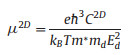
Geometric structures, including top and side views of SiP2 monolayer with an oblique lattice, are shown in Fig. 1, in which primary cell of the monolayer is composed of two P atoms and one Si atom. Optimized structure of SiP2 monolayer has the symmetry of space group P1 with the lattice parameters as a = 3.71Å, b = 3.74Å, α = 81.75°, β = 103.31° and γ = 97.56°. From Fig. 1b, the structure of monolayer is made up of septilateral rings and triangles labeled by P2, P1, Si1, while each Si atom forms four bonds exhibiting sp3 hybridization and each P atom forms three bonds also presenting sp3 hybridization. Moreover, the length of P-P bond in the structure is 2.269Å which is almost equal to that of 2.26Å in phosphorene[38], and the lengths of four Si-P bonds are 2.262, 2.274, 2.280 and 2.267Å respectively, slightly bigger than that of 2.254Å for the compound SiPH4 in previous results [39]. The contrasts of bonds show that the SiP2 monolayer does not demonstrate major differences with other analogous 2D structures, manifesting it is a stable 2D material.

|
Download:
|
| Fig. 1. (a) Top view of optimized lattice, (b) top view of SiP2 monolayer and (c) side view of SiP2 monolayer. | |
To demonstrate charge shift and formation of bonds in the SiP2 monolayer, we performed electron localization function (ELF) and bader analysis, and ELF plots are shown in Fig. 2 [40]. From the bader analysis, about -0.743 and -0.723 charges are shifted from the Si atom to two P atoms manifesting the formation of Si-P covalent bonds. From the top view in Fig. 2a, there exists electron collections between two P atoms and the Si atom, also indicating the formation of Si-P bonds. From the side view in Fig. 2b, one can find that alone pair of electrons exists for the P atoms, indicating the sp3 hybrid which leads to semiconducting features of the SiP2 monolayer [41].

|
Download:
|
| Fig. 2. (a) Top view and (b) side view of ELF plot of SiP2 monolayer with the isosurface of 0.88. | |
In order to inspect the stability of SiP2 monolayer, we calculated cohesive energy per atom (Ecoh), phonon dispersion, elastic constants and performed FPMD simulations, respectively. Firstly, we calculated Ecoh using the formula Ecoh = (mEP + nESi - EPmSin)/(m + n), where ESi, EP and EPmSin are energies of a Si atom, a P atom and SiP2 monolayer. Using this definition, Ecoh is computed as 1.65 eV/atom, and this value is similar to other monolayers, for example BP5, SixPy, g-BP and B2C monolayers [24, 42-44]. In consideration of the SiP2 monolayer is a compound of silicon and phosphorus elements with big atomic number, this result makes clear that it may be a potential stable phase of Si-P compounds.
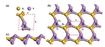
Secondly, to study dynamic stability of the SiP2 monolayer, we acquired its phonon spectrum which is shown in Fig. 3a. One can see that no negative phonon frequencies exist, manifesting the SiP2 monolayer to be indeed kinetically steady [5]. Moreover, the slopes of three acoustic branches are not identical along different orientations, such as G-X and G-Y, showing the SiP2 monolayer is anisotropic in regard to the in-plane stiffness, which can be also made clear in the discussions on in-plane stresses and carrier mobilities.

|
Download:
|
| Fig. 3. (a) Phonon spectrum and (b) FPMD simulation at room temperature 300 K of SiP2 monolayer. | |
Thirdly, to inspect thermal stability of the SiP2 monolayer, FPMD simulations were performed with a relatively large 4×4×1 supercell. As shown in Fig. S1 (Supporting information), through the 5ps simulation, the monolayer remains very well at 100, 300, 700 and 1000K, but is seriously distorted at 1100K. In view of the application of SiP2 monolayer, we further performed an equilibrium MD simulation at room temperature (300K) for 9ps, as shown in Fig. 3b, the energy is oscillating near the equilibrium state and the structure of SiP2 monolayer is preserved well. Likewise, these results suggest the thermal stability of SiP2 monolayer which is expected to be experimentally feasible.
Finally, we examine stability of the SiP2 monolayer by calculating the elastic constants(Cij), and a mechanically steady 2D structure should be in accord with the Born criteria [45]:

|
(1) |
By matching the energy bights correlated to in-plane stresses, Cij of SiP2 monolayer were derived to be C11=149.345N/m, C22=69.246N/m, C12=C21=-36.609N/m and C66=10.236N/m, which conform to the Born criteria, manifesting the mechanical stability of SiP2 monolayer. Using these elastic constants, in-plane Young's modules of SiP2 monolayer can be derived as Yx=(C11C22 - C12C21)/C22=129.99N/m andYy=(C11C22-C12C21)/C11=60.272N/m, which are smaller than that of graphene (~341N/m)[46] while almost the same as the value of MoS2 monolayer (~128N/m)[47], suggesting the monolayer should be a relatively hard material. The large imparity in two Young's modules also manifests that the SiP2 monolayer is mechanically anisotropic. Furthermore, it is well-known that most normal materials own normal Poisson's ratios, while materials with negative Poisson's ratios, which can transversely extend when stretched, are auxetic materials [48]. So the negative C12 of SiP2 monolayer makes negative Poisson's ratios νx = -0.529 (C21/C22) and νy=-0.245 (C12/C11), which are comparable to the δ-P monolayer and much larger than recently predicted 2D auxetic materials [49, 50]. The negative Poisson's ratios would demonstrate multiple superiority of SiP2 monolayer, for example the intensive tenacity, self-adaptive quaky damping and enhanced shear stiffness, and allow the SiP2 monolayer to be applied in many specific domains, such as superior dampers and nanoauxetic materials [45]. Moreover, there have presented experimental reports suggesting the negative Poisson's ratio of black phosphorene [51, 52]. Besides black phosphorene, other 2D materials have been reported as auxetic materials, such as BP5 monolayer [41], 2D Silicon Dioxide [53], Be2C [50], CaSi monolayer [45], δ-P monolayer [49], 1T-type crystalline two-dimensional TMDCs [54]. For the SiP2 monolayer, its negative Poisson's ratios may originate from its robust puckered structure which is shown in Fig.1c. The extraordinary mechanical properties of SiP2 monolayer would give it with infinite potential applications in nanomechanics and nanoelectronics.
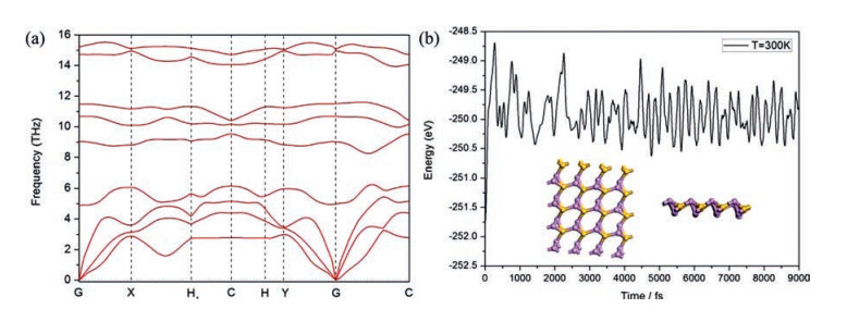
In Fig. 4, we show band structure and DOS of the SiP2 monolayer, and found the SiP2 monolayer is indirect with its band gap as 1.8484 eV (GGA-PBE) or 2.681 eV (HSE06). This value of band gap (> 2.0 eV) is larger than that of phosphorene and MoS2, and indicates more merit of SiP2 monolayer in the aspect of ultraviolet-blue optoelectronic materials [41, 55, 56]. Furthermore, DOS strength of P atoms is larger than the strength of Si atoms, while DOS strength for the p-orbital of total atoms are bigger than those for the s-orbital. Moreover from the figure, DOS strength at the point of CBM and VBM mainly come from p-orbital of P atoms, verifying that the carriers in the monolayer originate from P atoms as shown in Fig. 2.

|
Download:
|
| Fig. 4. Band structure and density of state (DOS) of SiP2 monolayer. | |
Applying stress is a general engineering strategy to acquire tunable band gaps, for example, MoS2 monolayer can reveal a direct-to-indirect transition with a uniaxial strain [57]. In light of this, we discuss effects of stresses to the band gap of SiP2 monolayer, and tensile strain lowers the puckering while contractile strain strengthens it [41, 42]. By changing the lattice parameters a and b in-plane biaxial and uniaxial stresses are utilized, and the strain ratio ε is defined as

|
(2) |
Under a strain for the strain ratio ε from -10% to 10%, effects of ε to the band gap of SiP2 monolayer are presented in Fig. S2 (Supporting information). From the figure, the value of band gap reduces when changing ε, and no indirect-to-direct transition exits for the SiP2 monolayer. Moreover, one can find that when ε is up to 3%, band gaps for biaxial and uniaxial cases reach the largest value, while the influences of biaxial strain are larger than those of uniaxial strain. This result may relate to the changes of pucker structure when exerting stresses to the SiP2 monolayer, and the effects of ε are similar to the phonon spectrum manifesting that the SiP2 monolayer is a mechanically anisotropic material. Furthermore, the largest value of band gap is 2.035 eV (PBE) for the biaxial strain case, while when ε for the biaxial case reduces to -9.5% or -10% the band gap fleetly reduces to zero presenting a semiconductor-to-metal transition. These consequences enhance applied opportunity of the SiP2 monolayer in optoelectronics and nanoelectronics using strain-engineering sciences[41, 56, 58, 59].
In Fig. 4, one can find CBM and VBM are located at C and (0.1020, 0.1020, 0.000) points with the energies as 2.892 and 4.740 eV respectively, and the carrier effective mass (EM) can be obtained accordingly. The carrier mobilities of SiP2 monolayer μ2D can be computed by taking advantage of following equation [60]
|
(3) |
where m* is EM, md is mean EM, T =300K, Ed is deformation potential (DP) constant and C2D is 2D Elastic Modulus, respectively.
Using above equations, calculated consequences with PBE functional are presented in Table 1. The carrier mobilities of SiP2 monolayer demonstrate strongly directional dependence, as well as the electron mobility along y orientation is much higher than that along x orientation and is significantly higher than those of two hole mobilities. Large disparity of electron and hole mobilities here originate from different DP constants rather than their EMs. Especially, the electron mobility along y orientation is ultrahigh (1.069×105 cm2 V-1 s-1), and this value is approximately four times the maximum value in phosphorene (0.26×105 cm2 V-1 s-1), significantly higher than the MoS2 (200 cm2 V-1 s-1) [61], almost the same as the CP monolayers (1.15×105 cm2 V-1 s-1) and slightly smaller than the graphene (2.0×105 cm2 V-1 s-1), respectively [62]. The huge carrier mobility of SiP2 monolayer further makes the monolayer as a hopeful 2D material in the domain of nanoelectronics.
|
|
Table 1 m*, Ed, C2D and μ2D along x or y orientation at 300 K. |

We further calculated absorption coefficient α(ω), energy loss spectrum (ELS) L(ω), reflectivity R(ω) of the SiP2 monolayer using following equations [63]:

|
(4) |
|
(5) |

|
(6) |
where ε(ω) = ε1(ω) + iε2(ω) is complex dielectric function.
From Fig. S3a (Supporting information) for two coefficients α(ω), the SiP2 monolayer presents distinguished absorption along two orientations with two excellent absorption peaks at 3.1 (400 nm) and 4.0 eV (310 nm), which cover significant interval of 2.0–4.5 eV including major visible and entire near-ultraviolet lights in the solar spectra. Moreover, α(ω) along the x and y orientations reach to the amount of 106 cm-1 which are similar to the coefficients of organic perovskite or crystalline silicon for solar cells [64, 65]. For the ELS L(ω) in Fig. S3b (Supporting information), they show one peak, on behalf of the energy of congregate stimulation excitation of carrier density [63]. For the reflectivity R(ω) in Fig. S3c (Supporting information), it attains to about 50% for E//x and E//y. These optical properties permit the SiP2 monolayer as a very promising material for efficient photovoltaic solar cells or optoelectronic devices.
Monolayer materials can be used as good catalytic materials [6, 66], so the adsorption of CO2 molecules was also studied here. The CO2 molecules were placed above the SiP2 based materials with different orientations to study the interaction between them. The adsorption energy (Eads) of CO2 on the SiP2 based materials was calculated by the following equation:

|
(7) |
where the ECO2-sub, Esub, ECO2 are the total energies of the CO2 adsorbed system in the equilibrium state, the substrate material and free CO2 molecule, respectively.
Five different chemical environments are considered here, as Figs. 5a and b shown, they are the top position of the P atom in the upper layer (P1), the top position of the P atom in the lower layer (the mountain valley position of the P and Si atom, P2), the top position of the Si atom in the middle layer (two valley position of P atoms S1), a triangular vacancy (H1) surrounded by two P atoms and one Si atom, and a hexagonal vacancy (H2) surrounded by four P atoms and three Si atoms, respectively. Next, the first-principle method was used to study the adsorption behavior of CO2 molecules on SiP2 monolayer. The above five possible adsorption sites have been explored for adsorption, and only the most stable adsorption structure at the H1 site with the adsorption energy of -0.28 eV was shown in Figs. 5c and d. The C, O atoms of CO2 molecule and the two P, one Si atoms at the H1 site merged a stable the penta-heterocycles structure, in which the angle of CO2 changed from 179.9° to 124.4° with the bond lengths of C–P and O-Si were shifted from 1.898Å to 1.728Å, respectively, indicating a chemical bond was formed between C–P and O-Si. This strong deformation means that CO2 was strongly chemically adsorbed on the SiP2 monolayer. In addition, the Hirshfeld charge transfer analysis of the adsorbed system indicated that the electrons transferred from SiP2 monolayer to the CO2 molecular, where the O and C atom involved in the five-membered ring got 0.077 and 0.181 e respectively, and the O atom not involved far away from the surface got 0.038e from SiP2 substrate. In addition, the difference charge densities diagram (Figs. 5e and f) of CO2 adsorbed on the SiP2 monolayer also point out that the composition of CO2 in the five-member ring is to form chemical bonds and there is a strong interaction. Furthermore, as shown in the Figs. 5e and f, the area between P and Si atoms connected to the CO2 appear blue, demonstrating that the electron density in CO2 adsorption increases, corresponding with the strong interaction between CO2 and SiP2 monolayer [67]. While region between C-O of CO2 is filled in yellow, showing that the charge density decreases as more electrons are transferred to the substrate.

|
Download:
|
| Fig. 5. (a, c) Top and (b, d) side views of calculated structure of 3 × 3×1 SiP2 supercell and CO2 adsorption on the SiP2 monolayer. Charge density difference for CO2 adsorption on SiP2 monolayer is shown in (e, f). The filling in blue and yellow represent increasing and decreasing electron densities. The value of isosurfaces is 0.05 e/Å3. | |
In order to explain the mechanism of CO2 adsorption on SiP2 monolayer, we introduced the Crystal Orbits Hamiltonian Population (COHP) to analyze the interaction of CO2 on SiP2 monolayer [68]. Taking the 0 point of COHP as the limit, the contribution of the anti-bonding orbits are filled in yellow above, and the contribution of the bonding orbits are filled in blue below. As can be seen from Figs. 6a and b, the bonding orbits of free CO2 molecules are mainly composed of the contributions of C 2s and O 2p, C 2p and O 2p, while the anti-bonding orbits are mainly composed of the contributions of O 2p, C 2s and C 2p. After CO2 adsorbed on SiP2 monolayer, it can be seen that the bonding orbital becomes mainly formed by O 2p and C 2p, and the bonding state as a whole transitions to a deeper level[69]. Integration Crystal Orbit Hamiltonian Population (ICOHP) is the integration of the energy interval to the highest occupied state, which can quantitatively represents the bonding strength [70]. Compared with free CO2, the ICOHP of C-O in adsorbed CO2 decreased from -18.71 to -10.85, indicating that the bonding strength between C-O was weakened, because more electrons between C-O were transferred to the substrate, resulting in weakened interaction. Similarly, as shown in Figs. 6c and d, it also shows that the interactions between the C and O atoms of CO2 and the P and Si atoms of SiP2 monolayer are enhanced, and their bonding states are mainly composed of C 2s and C 2p, P 3p, P 3s contribution (Fig. 6c), and composed with Si 3s and O 2p contribution (Fig. 6d). Therefore, one can see that if the SiP2 monolayer may be synthesized in experiments, it can be applied in solving the problem of global warming as a high-efficiency CO2 capturing material.

|
Download:
|
| Fig. 6. Project Density Of States (PDOS) and Crystal Orbital Hamilton Population (COHP) of (a) free CO2, (b) CO of CO2 after adsorption, (c) PC between C atom of CO2 and P atom of SiP2 monolayer, (d) O-Si between O atom of CO2 and Si atom of SiP2 monolayer. Blue stands for bonding contributions, while yellow stands for antibonding contributions. The fermi level is set at 0 eV. | |
In conclusion, by employing the PSO methodology within evolutionary algorithm, we obtained one SiP2 monolayer with its stability examined by cohesive energy, Born criteria, FPMD simulations and phonon spectrum, respectively. Our results indicate that the SiP2 monolayer is an indirect semiconductor with its band gap as 1.8484 (2.681) eV, as well as it is a relatively hard auxetic material with high negative Possion's ratios. Moreover, the SiP2 monolayer possesses an exceptional high carrier mobility which is comparable with those of the graphene and CP monolayers, and further CO2 molecules can be strongly chemically adsorbed on the SiP2 monolayer and a conversion from semiconductor to metal exists for -9.5% strain ratio case. These novel consequences exhibit the SiP2 monolayer owns a wide scope of applications in the high-performance optoelectronics, nanoelectronics, mechanics and CO2 capturing material.
Declaration of competing interestThe authors declare that they have no known competing financial interests or personal relationships that could have appeared to influence the work reported in this paper.
AcknowledgmentsThis study was funded by the Scientific Research Fund of Hunan Provincial Education Department of China (No. 16A081), the Natural Science Foundation of China (Nos. 21603109, 11304128), the Henan Joint Fund of the National Natural Science Foundation of China (No. U1404216), the Science and Technology Program of Henan Department of Science and Technology, China (No. 182102310609), and the Construct Program of Applied Characteristic Discipline in Hunan University of Science and Engineering (Mathematics, Electronic Science and Technology).
Appendix A. Supplementary dataSupplementary data associated with this article can be found, in the online version, at https://doi.org/10.1016/j.cclet.2020.08.031.
| [1] |
K.S. Novoselov, A.K. Geim, S.V. Morozov, et al., Science 306 (2004) 666-669. DOI:10.1126/science.1102896 |
| [2] |
Ch.Zh. He, R. Wang, H.Y. Yang, S. Li, L. Fu, Appl. Surf. Sci. 507 (2020) 145076. DOI:10.1016/j.apsusc.2019.145076 |
| [3] |
C.R. Ryder, J.D. Wood, S.A. Wells, M.C. Hersam, ACS Nano 10 (2016) 3900-3917. DOI:10.1021/acsnano.6b01091 |
| [4] |
X. Zhang, T. Li, Chin. Chem. Lett. 28 (2017) 2058-2064. DOI:10.1016/j.cclet.2017.09.008 |
| [5] |
G.C. Constantinescu, N.D.M. Hine, Nano Lett. 16 (2016) 2586-2594. DOI:10.1021/acs.nanolett.6b00154 |
| [6] |
S. Chandrasekaran, D.T. Ma, Y.Q. Ge, et al., Nano Energy 77 (2020) 105080. DOI:10.1016/j.nanoen.2020.105080 |
| [7] |
X.Y. Chia, M. Pumera, Nat. Catal. 1 (2018) 909-921. DOI:10.1038/s41929-018-0181-7 |
| [8] |
W. Cong, T. Yu, A. Bergara, et al., J. Phys. Chem. C 124 (2020) 4330-4337. DOI:10.1021/acs.jpcc.0c00494 |
| [9] |
M. Naseri, S. Lin, J. Jalilian, J. Gu, Z. Chen, Front. Phys. 13 (2018) 138102. DOI:10.1007/s11467-018-0758-2 |
| [10] |
C.S. Liu, X.Le. Yang, J. Liu, X.J. Ye, J. Phys. Chem. C 122 (2018) 22137-22142. DOI:10.1021/acs.jpcc.8b05529 |
| [11] |
L. Zhao, W.C. Yi, J. Botana, F.L. Gu, M.Sh. Miao, J. Phys. Chem. C 121 (2017) 28520-28526. DOI:10.1021/acs.jpcc.7b09650 |
| [12] |
M.C. Watts, L. Picco, F.S. Russell-Pavier, et al., Nature 568 (2019) 216-220. DOI:10.1038/s41586-019-1074-x |
| [13] |
Y.Y. Zhang, X.L. Zhang, Ch. Cheng, Z.X. Yang, Chin. Chem. Lett. 31 (2020) 931-936. DOI:10.1016/j.cclet.2019.12.010 |
| [14] |
W.C. Yi, X. Chen, X. Zh.Wang, et al., J. Mater. Chem. C Mater. Opt. Electron. Devices 7 (2019) 7352. DOI:10.1039/C9TC02030F |
| [15] |
Y. Jing, Y. Ma, Y. Li, T. Heine, Nano Lett. 17 (2017) 1833-1838. DOI:10.1021/acs.nanolett.6b05143 |
| [16] |
J.H. Yuan, A. Cresti, K.H. Xue, et al., J. Mater. Chem. C Mater. Opt. Electron. Devices 7 (2019) 639-644. DOI:10.1039/C8TC05164J |
| [17] |
B. Ghosh, S. Puri, A. Agarwal, S. Bhowmick, J. Phys. Chem. C 122 (2018) 18185-18191. DOI:10.1021/acs.jpcc.8b06668 |
| [18] |
S. Sun, F. Meng, H. Wang, H. Wang, Y. Ni, J. Mater. Chem. A Mater. Energy Sustain. 6 (2018) 11890-11897. DOI:10.1039/C8TA02494D |
| [19] |
N. Lu, Z. Zhuo, H. Guo, et al., J. Phys. Chem. Lett. 9 (2018) 1728-1733. DOI:10.1021/acs.jpclett.8b00595 |
| [20] |
T.E. Park, B.C. Min, L. Kim, et al., Nano Lett. 11 (2011) 4730-4735. DOI:10.1021/nl202535d |
| [21] |
K. Sato, A. Castaldini, N. Fukata, A. Cavallini, Nano Lett. 12 (2012) 3012-3017. DOI:10.1021/nl300802x |
| [22] |
N.J. Kramer, K.S. Schramke, U.R. Kortshagen, Nano Lett. 15 (2015) 5597-5603. DOI:10.1021/acs.nanolett.5b02287 |
| [23] |
J.G. Keizer, S. Koelling, P.M. Koenraad, M.Y. Simmons, ACS Nano 9 (2015) 12537-12541. DOI:10.1021/acsnano.5b06299 |
| [24] |
B. Huang, H.L. Zhuang, M.N. Yoon, B.G. Sumpter, Phys. Rev. B 91 (2015) 121401. DOI:10.1103/PhysRevB.91.121401 |
| [25] |
Y.C. Wang, M.S. Miao, J. Lv, et al., J. Chem. Phys. 137 (2012) 224108. DOI:10.1063/1.4769731 |
| [26] |
Y.C. Wang, Y.M. Ma, J. Chem. Phys. 140 (2014) 040901. DOI:10.1063/1.4861966 |
| [27] |
Y.C. Wang, J. Lv, L. Zhu, et al., J. Phys. Condens. Matter 27 (2015) 203203. DOI:10.1088/0953-8984/27/20/203203 |
| [28] |
H. Wang, Y.C. Wang, J. Lv, et al., Comp. Mater. Sci. 112 (2016) 406. DOI:10.1016/j.commatsci.2015.09.037 |
| [29] |
G. Kresse, J. Hafner, Phys. Rev. B 47 (1993) 558. DOI:10.1103/PhysRevB.47.558 |
| [30] |
G. Kresse, D. Joubert, Phys. Rev. B 59 (1999) 1758. |
| [31] |
J.P. Perdew, K. Burke, M. Ernzerhof, Phys. Rev. Lett. 77 (1996) 3865. DOI:10.1103/PhysRevLett.77.3865 |
| [32] |
G. Kresse, J. Furthmüller, Phys. Rev. B 54 (1996) 11169. DOI:10.1103/PhysRevB.54.11169 |
| [33] |
J. Paier, M. Marsman, K. Hummer, et al., J. Chem. Phys. 124 (2006) 154709. DOI:10.1063/1.2187006 |
| [34] |
A. Togo, I. Tanaka, Scr. Mater. 108 (2015) 1-5. DOI:10.1016/j.scriptamat.2015.07.021 |
| [35] |
B. Delley, J. Chem. Phys. 92 (1990) 508-517. DOI:10.1063/1.458452 |
| [36] |
K. Qi, X.Q. Cui, L. Gu, et al., Nat. Commun. 10 (2019) 5231. DOI:10.1038/s41467-019-12997-7 |
| [37] |
L. Sh.Yang, G. Lei, H.X. Xu, et al., Appl. Surf. Sci. 480 (2019) 205-211. DOI:10.1016/j.apsusc.2019.02.244 |
| [38] |
H. Liu, A.T. Neal, Z. Zhu, et al., ACS Nano 8 (2014) 4033-4041. DOI:10.1021/nn501226z |
| [39] |
A.G. Baboul, H.B. Schlegel, J. Am. Chem. Soc. 118 (1996) 8444-8451. DOI:10.1021/ja960771w |
| [40] |
E. Sanville, S.D. Kenny, R. Smith, G. Henkelman, J. Comput. Chem. 28 (2007) 899-908. DOI:10.1002/jcc.20575 |
| [41] |
S.J. Liu, B. Liu, X.H. Shi, et al., Sci. Rep. 7 (2017) 2404. DOI:10.1038/s41598-017-02011-9 |
| [42] |
H.D. Wang, X.X. Li, J.Y. Sun, Z. Liu, J.L. Yang, 2d Mater. 4 (2017) 045020. DOI:10.1088/2053-1583/aa8abd |
| [43] |
D.W. Zhou, P. Ch.Li, F.R. Yin, et al., Chin. Chem. Lett. 31 (2020) 2325-2329. DOI:10.1016/j.cclet.2020.04.045 |
| [44] |
Ch.Zh. He, R. Wang, D. Xiang, et al., Appl. Surf. Sci. 509 (2020) 145392. DOI:10.1016/j.apsusc.2020.145392 |
| [45] |
Y. Wang, M. Qiao, Yf. Li, Zf. Chen, Nanoscale Horiz. 3 (2018) 327-334. DOI:10.1039/C7NH00091J |
| [46] |
Q. Peng, X. Wen, S. De, RSC Adv. 3 (2013) 13772. DOI:10.1039/c3ra41347k |
| [47] |
Y.Q. Cai, G. Zhang, Y.W. Zhang, J. Am. Chem. Soc. 136 (2014) 6269-6275. DOI:10.1021/ja4109787 |
| [48] |
R.S. Lakes, Science 235 (1987) 1038-1040. DOI:10.1126/science.235.4792.1038 |
| [49] |
H. Wang, X. Li, P. Li, J.L. Yang, Nanoscale 9 (2017) 850-855. DOI:10.1039/C6NR08550D |
| [50] |
S.F. Qian, X.W. Sheng, Y. Zhou, et al., J. Phys. Chem. C 122 (2018) 7959-7967. DOI:10.1021/acs.jpcc.7b12758 |
| [51] |
Y.Ch. Du, J. Maassen, W.R. Wu, et al., Nano Lett. 16 (2016) 6701-6708. DOI:10.1021/acs.nanolett.6b03607 |
| [52] |
J.W. Jiang, H.S. Park, Nat. Commun. 5 (2014) 4727. DOI:10.1038/ncomms5727 |
| [53] |
Z.B. Gao, X. Dong, N.B. Li, J. Ren, Nano Lett. 8 (2008) 596-600. DOI:10.1021/nl072997a |
| [54] |
L.P. Yu, Q.M. Yan, A. Ruzsinszky, Nat. Commun. 8 (2017) 15224. DOI:10.1038/ncomms15224 |
| [55] |
Z.Y. Zhao, T. Yu, S.T. Zhang, et al., J. Mater. Chem. A Mater. Energy Sustain. 7 (2019) 405-411. DOI:10.1039/C8TA09155B |
| [56] |
S.L. Zhang, Z. Yan, Y.F. Li, Z.F. Chen, H.B. Zeng, Angew, Chem. Int. Ed 54 (2015) 3112-3115. DOI:10.1002/anie.201411246 |
| [57] |
N. Lu, H.Y. Guo, L. Li, et al., Nanoscale 6 (2014) 2879-2886. DOI:10.1039/C3NR06072A |
| [58] |
B. Rajbanshi, P. Sarkar, J. Phys. Chem. Lett. 8 (2017) 747-754. DOI:10.1021/acs.jpclett.6b02986 |
| [59] |
Y. Zhou, Z. Wang, P. Yang, et al., ACS Nano 6 (2012) 9727-9736. DOI:10.1021/nn303198w |
| [60] |
J. Bardeen, W. Shockley, Phys. Rev. 801 (2008) 72-80. |
| [61] |
B. Radisavljevic, A. Radenovic, J. Brivio, V. Giacometti, A. Kis, Nat. Nanotechnol. 6 (2011) 147-150. DOI:10.1038/nnano.2010.279 |
| [62] |
G.X. Wang, R. Pandey, S.P. Karna, Nanoscale 8 (2016) 8819-8825. DOI:10.1039/C6NR00498A |
| [63] |
B. Peng, H. Zhang, H.Z. Shao, et al., J. Mater. Chem. C Mater. Opt. Electron. Devices 4 (2016) 3592-3598. DOI:10.1039/C6TC00115G |
| [64] |
N.J. Jeon, J.H. Noh, Y.Ch. Kim, Nat. Mater. 13 (2014) 897-903. DOI:10.1038/nmat4014 |
| [65] |
M.A. Green, M.J. Keevers, Prog. Photovolt. 3 (1995) 189-192. DOI:10.1002/pip.4670030303 |
| [66] |
N. Li, X.Zh. Chen, W.J. Ong, et al., ACS Nano 11 (2017) 10825-10833. DOI:10.1021/acsnano.7b03738 |
| [67] |
M. Samadizadeh, A.A. Peyghan, S.F. Rastegar, Chin. Chem. Lett. 26 (2015) 1042-1045. DOI:10.1016/j.cclet.2015.05.048 |
| [68] |
R. Dronskowski, P.E. Bloechl, J. Phys. Chem. 97 (1993) 8617-8624. DOI:10.1021/j100135a014 |
| [69] |
S. Steinberg, R. Dronskowski, Crystals 8 (2018) 225. DOI:10.3390/cryst8050225 |
| [70] |
X. Liu, Y. Jiao, Y. Zheng, M. Jaroniec, S.Zh. Qiao, J. Am. Chem. Soc. 141 (2019) 9664-9672. DOI:10.1021/jacs.9b03811 |