 2021, Vol. 32


b College of Physics and Electronic Engineering, Nanyang Normal University, Nanyang 473061, China;
c Shaanxi Key Laboratory of Optoelectronic Functional Materials and Devices, School of Materials Science and Chemical Engineering, Xi'an Technological University, Xi'an 710021, China
The discovery of graphene [1] opens the door of two-dimensional (2D) materials, after that, a great deal of 2D materials such as hexagonal boron nitride [2], Mxenes [3-5], transitional-metal dichalcogenides (TMDs) [6, 7], and black phosphorene [8, 9] were discovered. Differ from their bulk counter-parts, 2D materials shows extraordinary properties and have great potentials for various applications including nanoelectronics and optoelectronics devices, field effect transistors (FET), sensor, p–n junctions, energy conversion and storage, and catalyst [10-16]. Especially, the 2D monolayer black phosphorene (BP), which can be mechanically exfoliated from black phosphorus and have a tunable thickness-dependent direct band gap and high carrier (hole) mobility, has emerged as a promising FET material [17-20]. Following the success of black phosphorene, 2D phosphides received increasing attention with both moderate band gaps and high carrier mobility. For example, the monolayer BP5 [21] with an indirect band gap (1.34 eV) exhibits an anisotropic visible-light absorption and high electron mobility of 7.1×103 cm2 V−1 s−1. 2D GeP3 [22] is also discovered to have the hole and electron mobility of 0.85×10⁴ and 0.88×104 cm 2 V−1 s−1, respectively. Other 2D phosphides such as 2D InP3 [23, 24], SnP3 [25, 26] and CaP3 [27] were also predicted to have high carrier mobility and have potential applications in optoelectronics and gas sensor.
2D materials also exhibit unique advantages as anodes due to their large surface-volume ratio, broad electrochemical window, fascinating chemical activity, and excellent mechanical strength. Some 2D materials (e.g., graphene [28], transition metal dichalcogenides [29], borophene [30, 31], phosphides [32]) have exhibited excellent performance in LIBs. However, the storage of lithium sources on Earth is rather limited. A potential candidate to replace LIBs is the rechargeable sodium-ion batteries (SIBs), which have attracted increasing attention because of the abundance of Na in earth (28, 400 mg/kg) [33] and low cost. Therefore, SIBs are deemed to be promising energy storage devices [34-38]. Up to now, a large number of 2D materials, such as graphene systems [39, 40], phosphorene [41, 42], borophene [43], transition-metal dichalcogenides and nitrides [44-48], and MXene [49, 50] have been explored as potential anode for SIBs. For example, phosphorene as anode in SIBs achieves the theoretical capacity of 865 mAh/g [41, 42], and borophene gain a maximum theoretical capacity of 1984 mAh/g [43]. Furthermore, there are extensive researches on searching for other 2D anode materials, including defective graphene (1450 mAh/g) [51], B-doped graphene (762 mAh/g) [52], nitrogen holey graphene (2469 mAh/g) [53], borocarbonitride based anode (810 mAh/g) [54], silicene, germanene and stanene (954, 369 and 226 mAh/g, respectively) [55, 56]. The ion diffusion barrier of most these 2D materials is in the range of 0.1 eV to 0.6 eV.
So the unique performances of 2D materials encourage more theoretical works to predict and design new 2D materials with novel properties for further expanding the 2D family. We noticed that the phosphorus-correlated 2D materials usually show good performances in both electronic properties and anode materials. In this paper, through a first principles swarm structural research, we design a stable 2D semiconductor material MgSiP2, which exhibits novel electronic properties and also shows outstanding electrode performance for SIBs. The MgSiP2 monolayer is an indirect-gap semiconductor with a band-gap of 1.20 eV. The mobility of electron and hole shows strong anisotropy. The electron mobility is as large as 1.29×104 cm2 V−1 s−1, while the hole mobility is very small. In addition, the predicted MgSiP2 show an ultrahigh theoretical storage capacity (1480 mAh/g) and small diffusion energy barriers (0.16 eV). The physical properties of MgSiP2 such as electronic properties are also discussed in this paper.
The 2D structure predictions of MgSiP2 monolayer are carried out using the particle-swarm optimization (PSO) method as implemented in the CALYPSO code [57, 58]. We performed structural searches with simulation cell sizes of 1, 2 and 4 formula units (f.u.). The 2D MgSiP2 were placed in the xy plane with the Z direction perpendicular to the layer plane. To make sure that there are no interactions among atoms along the Z direction, we use a very large vacuum layer of 30 Å during the 2D structure predictions. The structure optimization and electronic property calculations were performed with projector augmented wave (PAW) method [59, 60] as implemented in the Vienna ab-initio simulation package (VASP) [61, 62]. The generalized gradient approximation (GGA) with Perdew-Burke-Ernzerhof (PBE) [63] function was adopted for the exchange-correlation functional. To estimate the band structures of MgSiP2 more accurately, the Heyd–Scuseria–Ernzerhof (HSE06) hybrid functional [64] with the screening parameter (ω) of 0.2 Å−1 was used. The plane wave cutoff energy of 600 eV was employed in all the computations. The convergence threshold was set as 10−6 eV in energy and 10−3 eV in force. The Brillouin zone was sampled with a 9×16×1 Monkhorst-Pack k-point grid. The phonon dispersion curves were calculated with the finite displacement method implemented in the phonopy package [65]. The thermal stability was further tested by ab initio molecular dynamics (AIMD) simulations using the canonical ensemble (NVT) with a 2×3 supercell. In the calculation of Na-ion adsorption, we set 35 Å vacuum layer to avoid interactions between the neighboring images under the periodic boundary condition. To quantitatively determine the lowest energetic diffusion pathways of Na on MgSiP2, we used the climbing Nudged Elastic Band method (cNEB) method [66].
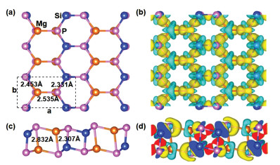
The most stable structure of MgSiP2 through the global structure searching is shown in Fig. 1a (top view) and Fig. 1c (side view). We can see that the 2D structure exhibits bilayer stacking system of a low-buckled honeycomb lattice. Two dimensional MgSiP2 has a space group of P2/m (No.10) and the unit cell of MgSiP2 contains two Mg, two Si and four P atoms in a monoclinic with lattice constants of a=7.211 and b =3.796 Å. Each Si atom and Mg atom binds to four P atoms forming silicon-phosphorus and magnesium-phosphorus tetrahedron, respectively. The Si-P bond lengths are 2.307 and 2.331 Å, where the bond distances of Mg-P are 2.453, 2.535 and 2.832 Å, respectively, indicating that the magnesium atom and silicon atom can't form the standard sp3 configuration.

|
Download:
|
| Fig. 1. Schematic illustration of two dimensional MgSiP2 (a) top view and (c) side view, Mg, Si and P atoms are represented by brown, blue, and pink spheres, respectively. Difference charge density plots (b) top view and (d) side view. The gold color (i.e., 0.006 e/Å3) in the plot indicates an electron density increase in the electron density after bonding, and the cyan color (i.e., 0.006 e/Å3) indicates a loss. | |
The chemical bonding of the MgSiP2 can be understood according to its charge difference density (Figs. 1b and d), which is defined as the total electron density of the MgSiP2 minus the electron density of isolated Mg, Si and P atoms at their respective positions. It is clearly seen from Figs. 1b and d that a significant amount of electrons transfers from Mg to the nearest and next-nearest P atoms. Our Bader charge analysis suggests that the Mg-P bonds are more ionic in nature as net charges on Mg are +1.52|e|, while the atoms between Si-P are covalently bonded.
To clarify the thermal stability of the predicted 2D MgSiP2, we calculated its formation energy defined ass

|
(1) |
where E2d(MgSiP2), E2d(SiP2), and Ebulk(Mg) are the total energies of 2D MgSiP2, 2D SiP2 reported in the previous work [67], and the bulk hcp-Mg material, respectively. n2d(MgSiP2), n2d(SiP2) and nbulk(Mg) are the number of atoms present in the unit cell considered for the calculation. The calculated formation energy for the MgSiP2 monolayer is -0.49 eV per f.u. The negative formation energy implies that the synthesis of the MgSiP2 monolayer under ambient conditions is feasible.
The dynamical stability of MgSiP2 was also checked by calculating the phonon dispersion curves. As shown in Fig. S1a (Supporting information), no imaginary frequency in the first Brillouin zone was found, which confirms the dynamical stability of MgSiP2. To further evaluate the thermal stability, we performed AIMD simulations of the MgSiP2 with a 2×3 supercell at the temperature of 600 K and 900 K. The fluctuation of the total potential energy with simulation time is plotted in Fig. S1b (Supporting information) and Fig. S1c (Supporting information), respectively, which shows that the average value of the total potential energy remains nearly constant during the entire simulation. Snapshots taken at the end of 10 ps are also shown in Figs. S1b and c, respectively. From the snapshots, one can see that the original geometry of MgSiP2 is generally well-kept and no bond is broken at 600 K. As temperature increase to 900 K, the distortion become more and more evident and the framework of MgSiP2 started to collapse. The above results reveal that the MgSiP2 monolayer can maintain its structural integrity even at a temperature of 600 K.
The mechanical stability of MgSiP2 was examine, and the four independent elastic constants C11, C22, C12 and C66 are calculated to be C11 = 83.7 N/m, C22 = 81.0 N/m, C12 = 25.5 N/m and C66 = 10.1 N/m, respectively. All the calculated elastic constants meet the necessary mechanical equilibrium conditions [68] for mechanical stability: C11C22 - C122 > 0 and C11, C22 and C66 > 0. Thus the 2D MgSiP2 also meet mechanical stability criteria.
To get insight into the electronic properties of MgSiP2, the calculated band structure together with its projected density of states are shown in Fig. S2a (Supporting information). The calculation of energy band structure reveals that MgSiP2 is an indirect band gap semiconductor. The conduction band minimum (CBM) is located at S point, while the valence band maximum (VBM) is located at the Γ point. The band gap of MgSiP2 is 0.51 eV by the PBE calculation. Due to the band gap underestimation of PBE, we have also estimated the band gap using the non-local hybrid functional, and the obtained band gap value of 1.20 eV. The suitable band gap width makes the 2D MgSiP2 might can be used to solar cell device. Furthermore, anisotropic band-structured features can be seen from Fig. S2a, the lowest conduct band has a very large dispersion in both S-X and S-Y directions, whereas the highest valence band is very flat in the Γ-X direction. As we all known, the larger the band curvature, the smaller the effective mass, and this is true reciprocally. So the 2D MgSiP2 has a very small effective mass of electron, while a very large effective mass of the hole in the Γ-X direction. In fact, the small effective mass of electron of MgSiP2 results in large electron mobility and we will discuss later. We also pointed out that the larger difference effective mass between electron and hole is usually favorable to reduce electron-hole recombination rate, suggesting the 2D MgSiP2 may also show good performance as a photochemical catalysis material.
The projected densities of states (PDOS) show that the VBM are mainly contributed by the P 2p states, while the unoccupied conduction band is contributed by the hybridized 3s and 3p orbitals of Si and P atoms. The partial charge densities associated with the VBM and CBM (Figs. S2b and c in Supporting information) for MgSiP2 reveal that the VBM mainly distributes on the P atoms nearest to Si atoms, while the CBM mainly distributes on both P and Si atoms and the middle of a square consisting of Si and P atoms. Therefore, the Si and P atoms could provide empty orbitals for electron-donor alkali metal and could have better adsorption capacity for alkali metal atoms, suggesting that 2D MgSiP2 can be used to design high-performance alkali-metal-ion batteries.
We further evaluate the effective mass and carrier mobility of MgSiP2 quantitatively based on the calculated band structure along a and b directions. Schematic of structure of MgSiP2 is shown in Fig. 2a. However, since the hole effective mass along a direction is very large, we only calculated the effective mass of the electron by fitting the band dispersion along a and b directions and hole along b direction to the following formula:
|
(2) |

|
Download:
|
| Fig. 2. (a) Schematic of the strain along the a and b directions. (b) The total energy shift as a function of lattice deformation along a and b directions in MgSiP2. (c) Shift of the conduction band under uniaxial strain along the a direction and b direction. (d) Shift of the valence band under uniaxial strain along the b direction. | |
The effective masses are calculated to be 0.385 m0 (0.258 m0) for electron along the a(b) direction and 0.156m0 for hole along the b direction, where m0 is the effective mass of a free electron. The effective mass of electron is different along the a and b directions. So the effective mass of electron is anisotropic, and the effective mass along the a direction is higher than that along the b direction.
The carrier mobility of MgSiP2 were described by the deformation potential approximation [69] using the following formula [70]:

|
(3) |
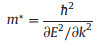
where m* is the effective mass in the transport direction, T is the temperature of 300 K, is the deformation potential constant. C2d is the elastic modulus derived from 
The changes of total energy versus strains are shown in Fig.2b. We obtained the in-plane stiffness C2d by fitting the energy-strain curves. The C2d are 83.3 and 81.5 N/m for a and b directions, respectively. The shift of band edges as a function of strain is shown in Figs. 2c and d. The deformation potentials are equal to the slope of the fitting lines. Based on the obtained Eli, C2d and m*, the mobility at T = 300 K are calculated and listed inTable 1. The electron mobility of MgSiP2 are predicted to be 2.50×10³ and 1.29×104 cm2 V−1 s−1 along a direction and b direction, respectively. The hole mobility is only 837 cm2 V−1 s−1 along the b direction. The electron mobility of 2D MgSiP2 along b direction is significantly higher than that of MoS2 mono-layer nanosheets (~200 cm2 V−1 s−1) [71] and can comparable with that of XP3 (X=Ca, In, Ge and Sb) [22-27, 72], which suggests its promising potential applications in nanoelectronics. We want to pointed that the large carrier mobility (electrons along b direction) originates from the small deformation potential constant E1 of the conduction band. The MgSiP2 has high carrier mobility along b direction than that along a direction, which shown an anisotropic character in-plane.
|
|
Table 1 Calculated deformation potential constant (El), 2D elastic modulus (C2d), effective mass (m*), and mobility for electron (e) and hole (h) along a and b directions at 300 K. |
Since both silicon and phosphorus elements show good integration with sodium, 2D Phosphorene and silicene exhibit large capacities as anode sodium battery. Considering the elemental and structural similarity, we further estimated the performance of MgSiP2 as an anode material.
We first estimated Na absorption behaviors on 2D MgSiP2 using a 2×3 supercell as the substrate, which is tested to be large enough to weaken their interactions. After adsorption of one Na atom, the adsorption energy Eads is calculated using the following formula

|
(4) |
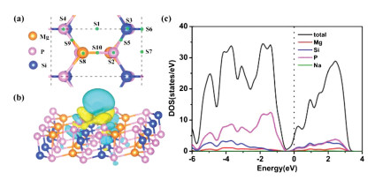
where ENa+MgSiP2 and EMgSiP2 refer to the total energy of MgSiP2 with and without adsorbed Na atom, respectively, ENa represents the average energy of a Na atom in bulk Na metal. Considering the structural symmetry of MgSiP2 lattice, nine possible sites for Na atom adsorption are shown in Fig. 3a. After the geometry optimizations of the adsorbed MgSiP2 systems, we found that some Na atoms would spontaneously transfer from one site to another site, and the equivalent sites are listed as following: S2=S1, S3=S4 = S5=S6, S8=S9 = S10. So only S1, S3, S7 and S8 sites are left. The adsorbed energies for Na atoms are calculated to be −0.581 eV (S1), −0.611 eV (S3), −0.720 eV (S7), and −0.357 eV (S8), respectively. The negative Eads for all four sites indicates the dispersive distribution of adsorbed Na atoms instead of forming a cluster.

|
Download:
|
| Fig. 3. (a) The possible sites for Na adsorption of 2D MgSiP2 material. (b) The charge density difference Δρ with the absorption of Na atom with the isosurface level of 0.001 e/Å3. (c) The total and partial density of states of MgSiP2Na. | |
To get better understanding of electronic interactions between Na ions and MgSiP2 electrode, we have investigated the charge density difference between metal ions and MgSiP2, as presented in Fig. 3b. The charge density difference can be expressed as Δρ=ρNaMgSiP2 - ρMgSiP2 - ρNa, where ρNaMgSiP2, ρMgSiP2 and ρNa refer to the charge density of MgSiP2 layer with adsorbed Na atom, pristine MgSiP2 and the isolated Na atom, respectively. The cyan and yellow areas represent electron depletion and accumulation, respectively. Obvious electron localization can be observed with remarkable electron accumulation around P atoms and depletion around the metal atoms, which indicates the formation of the strong ionic bond. The total and partial density of states of NaMgSiP2 are also shown in Fig. 3c. It can be seen that there are considerable electronic states at the Fermi level, which indicates that the adsorption of Na atom changes 2D MgSiP2 from a semiconductor to a metal. The metal character of NaMgSiP2 is also advantageous for making 2D MgSiP2 electrode material.
The storage capacity is one of the most concerned parameters for the electrode materials. In order to calculate the storage capacity, we first calculated the average adsorption energy layer by layer, which is defined by
|
(5) |
where ENa is the total energy per atom in bulk Na, while ENa12nMg12Si12P24 and ENa12(n-1)Mg12Si12P24 represent the total energies of EMg12Si12P24 (2×3 supercell of MgSiP2) with the absorption of n and n-1 Na atom layers, respectively. If is negative, then the adsorption of n layers is more favorable energetically rather than forming Na clusters. The one-layer, two-layer, and three-layer adsorptions of Na atoms on both sides of 2×3 supercell of 2D MgSiP2 were estimated. As shown in Fig. S3 (Supporting information), for the first adsorption layer, the metal atoms are adsorbed above the vacancies S1 and S7, which is the most stable Na adsorption sites with the lowest energy. The corresponding adsorption energy for the first adsorption layer is calculated to be −0.324 eV. For the second adsorption layer, the S3 and S4 sites are found to be the most stable adsorption sites, and the adsorption energy is −0.148 eV. When the third layer Na atoms is added, the S1 and S7 becomes the most stable adsorption sites again, the absorption energy still can keep negative with a value of −0.011 eV. However, when the fourth layer is added, the absorption energy becomes a positive value of 0.02 eV. So MgSiP2 can adsorb maximum three layers of Na atoms in theory. Then we can calculate maximum capacity (CM) by the following equation

|
(6) |
where x represents the number of adsorbed Na ions on the MgSiP2 per formula unit, F derives from the Faraday constant with the value of 26, 798 mAh/mol, and M is the mass of MgSiP2 in g/mol. The stoichiometry MgSiP2Na6 reaches a maximum theoretical capacity of 1406.2 mAh/g, Even if the final product of sodium could not achieves MgSiP2Na6, the stable MgSiP2Na4 stoichiometry can also get a theoretical capacity of 937 mAh/g. The capacity of MgSiP2 is much higher than that of reported 2D anode materials (e.g., 132 mAh/g for Mo2C [73], 146 mAh/g for MoS2 [46], 253 mAh/g SnP3 [74] and 751 mAh/g for ReN2 [75]). We also estimated the volume changes of sodiation MgSiP2. According to previous work, although some 2D materials such as Si and P have a large capacity, however, the huge volume change of Si limited their application as good anodes. For MgSiP2, the volume change is within 9.5% with the increasing of Na adsorbing layers. The small change in volume after the adsorption of one, two and three layers of Na ions indicates that the MgSiP2 is robust.
We further turn our focus on the open circuit voltage (OCV) in fact, the charge/discharge process of MgSiP2 can be described as

|
(7) |
Based on this reaction, the average open circuit voltage can be defined by
|
(8) |
where ENanMgSiP2 and EMgSiP2 refer to the total energy of MgSiP2 with and without adsorbed Na atom, respectively, n and represents the number of Na atom and average energy of a Na atom in bulk Na metal assuming volume and entropy effects are negligible. The calculated OCV value decreases from 0.23 V to 0.15 V with the increase of the adsorbed Na concentration from 48 atoms to 72 atoms on the 2×3 supercell. So the MgSiP2 is suitable to serve as an anode material because of its relatively low average OCV.
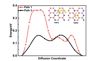
The diffusion barrier of metal ion is as essential parameter to estimate the performance of the battery. A low diffusion barrier means a fast charging/discharging process for ion batteries. We first investigate the diffusion of one Na ion on the MgSiP2 surface. Two possible diffusion paths between the lowest energy adsorption sites and the calculated results are shown in Fig. 4. The diffusion barrier of the path 1 is 0.16 eV, which lower than that of path 2 (0.36 eV) and other anode materials, such as BP (0.22 eV) [76], MoN2 (0.56 eV) [77], NiC3 (0.23 eV) [78] comparable with that of TiC3 (0.18 eV) [79], P3C (0.19 eV) [80] and ReS2 (0.16 eV) [81]. The low diffusion can result in ultrafast charging/discharging cycles in the Na ion batteries.

|
Download:
|
| Fig. 4. Energy profile of Na diffusion on path 1 and path 2. The inserted figures show the possible sites for Na adsorption in MgSiP2, and the corresponding diffusion pathways are also shown. | |
In summary, we predicted a stable 2D MgSiP2 with bilayer stacking system of a low-buckled honeycomb lattice by using the PSO-based global structure search method and first-principles calculations. The phonon spectrum, molecular dynamics, and elastic constants simulation confirm its dynamical, thermal, and mechanical stabilities, respectively. It has an indirect band gap with the value of 1.20 eV, which is promising candidate for solar cell. The highest electron mobility (1.29×104 cm2 V−1 s−1) of MgSiP2 is comparable with that of XP3 (X=Ca, Ge, Sb), showing the potential application in nano electronic devices. Furthermore, we investigate 2D MgSiP2 as an anode for NIBs. The metallicity of the MgSiP2 with Na adsorption provides good electron conductivity. The MgSiP2 can spontaneously adsorb Na ions with an unexpected stoichiometry of Na6MgSiP2, leading to a large theoretical capacity of 1406 mAh/g. Its Na ion diffusion barrier is as low as 0.16 eV, ensuring a quick charge/discharge rate capacity for SIBs. These results could enhance the understanding of 2D MgSiP2, which is important for the designing of anode materials for SIBs.
Declaration of competing interestThe authors report no declarations of interest.
AcknowledgmentsThis research was supported by Henan Joint Funds of the National Natural Science Foundation of China (Nos. U1904179, U1404608 and U1404216), the National Natural Science Foundation of China (No. 21603109), the Key Science Fund of Educational Department of Henan Province of China (No. 20B140010).
Appendix A. Supplementary dataSupplementary material related to this article can be found, in the online version, at doi:https://doi.org/10.1016/j.cclet.2020.08.042.
| [1] |
K.S. Novoselov, A.K. Geim, S.V. Morozov, et al., Science 306 (2004) 666-669. DOI:10.1126/science.1102896 |
| [2] |
L. Song, L.J. Ci, H. Lu, et al., Nano Lett. 10 (2010) 3209-3215. DOI:10.1021/nl1022139 |
| [3] |
M. Naguib, M. Kurtoglu, V. Presser, et al., Adv. Mater. 23 (2011) 4248-4253. DOI:10.1002/adma.201102306 |
| [4] |
Z. Guo, J. Zhou, L. Zhu, et al., J. Mater. Chem. A 4 (2016) 11446-11452. DOI:10.1039/C6TA04414J |
| [5] |
Z. Guo, N. Miao, J. Zhou, et al., J. Mater. Chem. C 5 (2017) 978-984. DOI:10.1039/C6TC04349F |
| [6] |
Q.H. Wang, Kalantar-Zadeh K., A. Kis, et al., Nat. Nanotechnol. 7 (2012) 699-712. DOI:10.1038/nnano.2012.193 |
| [7] |
Q. Peng, Z. Wang, B. Sa, et al., Sci. Rep. 6 (2016) 31994. DOI:10.1038/srep31994 |
| [8] |
R. Fei, L. Yang, Nano Lett. 14 (2014) 2884-2889. DOI:10.1021/nl500935z |
| [9] |
M. Buscema, D.J. Groenendijk, S.L. Blanter, et al., Nano Lett. 14 (2014) 3347-3352. DOI:10.1021/nl5008085 |
| [10] |
L. Liao, Y.C. Lin, M.Q. Bao, et al., Nature 467 (2010) 305-308. DOI:10.1038/nature09405 |
| [11] |
M.Y. Li, Y. Shi, C.C. Cheng, et al., Science 349 (2015) 524-528. DOI:10.1126/science.aab4097 |
| [12] |
Y. Wen, F. Wei, W. Zhang, et al., Chin. Chem. Lett. 31 (2020) 521-524. DOI:10.1016/j.cclet.2019.04.071 |
| [13] |
Y. Li, X. Wang, C.Y. Xing, et al., Chin. Chem. Lett. 30 (2019) 1440-1444. DOI:10.1016/j.cclet.2019.03.014 |
| [14] |
S. Ahmad, X. Guo, Chin. Chem. Lett. 29 (2018) 657-663. DOI:10.1016/j.cclet.2017.08.057 |
| [15] |
B. Xu, S. Qi, M. Jin, et al., Chin. Chem. Lett. 30 (2019) 2053-2064. DOI:10.1016/j.cclet.2019.10.028 |
| [16] |
G. Liu, J. Zhou, W. Zhao, et al., Chin. Chem. Lett. 31 (2020) 1966-1969. DOI:10.1016/j.cclet.2019.12.023 |
| [17] |
J. Qiao, X. Kong, Z.X. Hu, et al., Nature Commun. 5 (2014) 4475. DOI:10.1038/ncomms5475 |
| [18] |
H. Liu, Y. Du, Y. Deng, et al., Chem. Soc. Rev. 44 (2015) 2732-2743. DOI:10.1039/C4CS00257A |
| [19] |
L. Kou, C. Chen, S.C. Smith, J. Phys. Chem. Lett. 6 (2015) 2794-2805. DOI:10.1021/acs.jpclett.5b01094 |
| [20] |
Y.Y. Illarionov, M. Waltl, G. Rzepa, et al., ACS Nano 10 (2016) 9543-9549. DOI:10.1021/acsnano.6b04814 |
| [21] |
H. Wang, X. Li, J. Sun, et al., 2D Materials 4 (2017) 045020. DOI:10.1088/2053-1583/aa8abd |
| [22] |
Y. Jing, Y. Ma, Y. Li, et al., Nano Lett. 17 (2017) 1833-1838. DOI:10.1021/acs.nanolett.6b05143 |
| [23] |
N. Miao, B. Xu, N.C. Bristowe, et al., J. Am. Chem. Soc. 139 (2017) 11125-11131. DOI:10.1021/jacs.7b05133 |
| [24] |
W. Yi, X. Chen, Z. Wang, et al., J. Mater. Chem. C 7 (2019) 7352-7359. DOI:10.1039/C9TC02030F |
| [25] |
B. Ghosh, S. Puri, A. Agarwal, et al., J. Phys. Chem. C 122 (2018) 18185-18191. DOI:10.1021/acs.jpcc.8b06668 |
| [26] |
S. Sun, F. Meng, H. Wang, et al., J. Mater. Chem. A 6 (2018) 11890-11897. DOI:10.1039/C8TA02494D |
| [27] |
N. Lu, Z. Zhuo, H. Guo, et al., J. Phys. Chem. Lett. 9 (2018) 1728-1733. DOI:10.1021/acs.jpclett.8b00595 |
| [28] |
E. Lee, K.A. Persson, Nano Lett. 12 (2012) 4624-4628. DOI:10.1021/nl3019164 |
| [29] |
M. Chhowalla, H.S. Shin, G. Eda, et al., Nat. Chem. 5 (2013) 263-275. DOI:10.1038/nchem.1589 |
| [30] |
H.R. Jiang, Z. Lu, M.C. Wu, et al., Nano Energy 23 (2016) 97-104. DOI:10.1016/j.nanoen.2016.03.013 |
| [31] |
D. Rao, L. Zhang, Z. Meng, et al., J. Mater. Chem. A 5 (2017) 2328-2338. DOI:10.1039/C6TA09730H |
| [32] |
J. Lin, T. Yu, F. Han, et al., WIREs Comput. Mol. Sci. (2020). DOI:10.1002/wcms.1473 |
| [33] |
S. Mukherjee, L. Kavalsky, C.V. Singh, ACS Appl. Mater. Interfaces 10 (2018) 8630-8639. DOI:10.1021/acsami.7b18595 |
| [34] |
X. Xie, Z. Ao, D. Su, et al., Adv. Funct. Mater. 25 (2015) 1393-1403. DOI:10.1002/adfm.201404078 |
| [35] |
M. Li, B. Sun, Z. Ao, et al., J. Mater. Chem. A 8 (2020) 10199-10205. DOI:10.1039/D0TA01853H |
| [36] |
Z. Yan, Q. Yang, Q. Wang, et al., Chin. Chem. Lett. 31 (2020) 583-588. DOI:10.1016/j.cclet.2019.11.002 |
| [37] |
S. Qi, B. Xu, V. Tiong, et al., Chem. Eng. J. 379 (2020) 122261. DOI:10.1016/j.cej.2019.122261 |
| [38] |
B. Xu, S. Qi, P. He, et al., Chem. Asian J. 14 (2019) 2925-2937. DOI:10.1002/asia.201900784 |
| [39] |
X. Qian, X. Gu, M.S. Dresselhaus, et al., J. Phys. Chem. Lett. 7 (2016) 4744-4750. DOI:10.1021/acs.jpclett.6b02295 |
| [40] |
L. Shi, T.S. Zhao, A. Xu, et al., J. Mater. Chem. A 4 (2016) 16377-16382. DOI:10.1039/C6TA06976B |
| [41] |
V.V. Kulish, O.I. Malyi, C. Persson, et al., Phys. Chem. Chem. Phys. 17 (2015) 13921-13928. DOI:10.1039/C5CP01502B |
| [42] |
K.P.S.S. Hembram, H. Jung, B.C. Yeo, et al., J. Phys. Chem. C 119 (2015) 15041-15046. DOI:10.1021/acs.jpcc.5b05482 |
| [43] |
X. Zhang, J. Hu, Y. Cheng, et al., Nanoscale 8 (2016) 15340-15347. DOI:10.1039/C6NR04186H |
| [44] |
E. Yang, H. Ji, Y. Jung, J. Phys. Chem. C 119 (2015) 26374-26380. DOI:10.1021/acs.jpcc.5b09935 |
| [45] |
X. Huang, Z. Zeng, H. Zhang, Chem. Soc. Rev. 42 (2013) 1934-1946. DOI:10.1039/c2cs35387c |
| [46] |
M. Mortazavi, C. Wang, J. Deng, et al., J. Power Sources 268 (2014) 279-286. DOI:10.1016/j.jpowsour.2014.06.049 |
| [47] |
X. Lv, W. Wei, Q. Sun, et al., J. Phys. D: Appl. Phys. 50 (2017) 235501. DOI:10.1088/1361-6463/aa6eca |
| [48] |
A. Samad, Y.H. Shin, ACS Appl. Mater. Interfaces 9 (2017) 29942-29949. DOI:10.1021/acsami.7b07161 |
| [49] |
Q. Meng, A. Hu, C. Zhi, et al., Phys. Chem. Chem. Phys. 19 (2017) 29106-29113. DOI:10.1039/C7CP06171D |
| [50] |
D. Er, J. Li, M. Naguib, et al., ACS Appl. Mater. Interfaces 6 (2014) 11173-11179. DOI:10.1021/am501144q |
| [51] |
D. Datta, J.W. Li, V.B. Shenoy, ACS Appl. Mater. Interfaces 6 (2014) 1788-1795. DOI:10.1021/am404788e |
| [52] |
C. Ling, F. Mizuno, Phys. Chem. Chem. Phys. 16 (2014) 10419-10424. DOI:10.1039/C4CP01045K |
| [53] |
D. Wu, B. Yang, E. Ruckenstein, et al., J. Phys. Chem. Lett. 10 (2019) 721-726. DOI:10.1021/acs.jpclett.8b03435 |
| [54] |
S. Banerjee, S. Neihsial, S.K. Pati, J. Mater. Chem. A 4 (2016) 5517-5527. DOI:10.1039/C6TA01645F |
| [55] |
J. Zhu, U. Schwingenschlögl, 2D Materials 3 (2016) 035012. DOI:10.1088/2053-1583/3/3/035012 |
| [56] |
B. Mortazavi, A. Dianat, G. Cuniberti, et al., Electrochim. Acta 213 (2016) 865-870. DOI:10.1016/j.electacta.2016.08.027 |
| [57] |
B. Gao, P. Gao, S. Lu, et al., Sci.Bull. 64 (2019) 301-309. DOI:10.1016/j.scib.2019.02.009 |
| [58] |
Y. Wang, J. Lv, L. Zhu, et al., Phys. Rev. B: Condens. Matter Mater. Phys. 82 (2010) 094116. DOI:10.1103/PhysRevB.82.094116 |
| [59] |
P.E. Blöchl, Phys. Rev. B: Condens. Matter Mater. Phys. 50 (1994) 17953-17979. DOI:10.1103/PhysRevB.50.17953 |
| [60] |
G. Kresse, D. Joubert, Phys. Rev. B 59 (1999) 1758-1775. DOI:10.1016/j.jallcom.2013.08.073 |
| [61] |
G. Kresse, J. Hafner, Phys. Rev. B: Condens. Matter Mater. Phys. 48 (1993) 13115-13118. DOI:10.1103/PhysRevB.48.13115 |
| [62] |
G. Kresse, J. Furthmuller, Phys. Rev. B: Condens. Matter Mater. Phys. 54 (1996) 11169-11186. DOI:10.1103/PhysRevB.54.11169 |
| [63] |
J.P. Perdew, K. Burke, M. Ernzerhof, Phys. Rev. Lett. 77 (1996) 3865. DOI:10.1103/PhysRevLett.77.3865 |
| [64] |
J. Heyd, G.E. Scuseria, M. Ernzerhof, J. Chem. Phys. 118 (2003) 8207-8215. DOI:10.1063/1.1564060 |
| [65] |
M.D. Segall, P.J.D. Lindan, M.J. Probert, et al., J. Phys.: Condens. Matter 14 (2002) 2717-2744. DOI:10.1088/0953-8984/14/11/301 |
| [66] |
G. Henkelman, B.P. Uberuaga, H. Jónsson, J. Chem. Phys. 113 (2000) 9901-9904. DOI:10.1063/1.1329672 |
| [67] |
B. Huang, H.L. Zhuang, M. Yoon, et al., Phys. Rev. 91 (2015) 121401. DOI:10.1103/PhysRevB.91.121401 |
| [68] |
F. Mouhat, F.X. Coudert, Phys. Rev. 90 (2014) 224104. DOI:10.1103/PhysRevB.90.224104 |
| [69] |
J. Bardeen, W. Shockley, Phys. Rev. 80 (1950) 72-80. DOI:10.1103/PhysRev.80.72 |
| [70] |
C. Zhang, Q. Sun, J. Phys. Chem. Lett. 7 (2016) 2664-2670. DOI:10.1021/acs.jpclett.6b01291 |
| [71] |
B. Radisavljevic, A. Radenovic, J. Brivio, et al., Nat. Nanotechnol. 6 (2011) 147-150. DOI:10.1038/nnano.2010.279 |
| [72] |
S. Yao, X. Zhang, Z. Zhang, et al., Int. J. Hydrogen Energy 44 (2019) 5948-5954. DOI:10.1016/j.ijhydene.2019.01.106 |
| [73] |
Q. Sun, Y. Dai, Y. Ma, et al., J. Phys. Chem. Lett. 7 (2016) 937-943. DOI:10.1021/acs.jpclett.6b00171 |
| [74] |
C.S. Liu, X.L. Yang, J. Liu, et al., ACS Appl. Mater. Interfaces 1 (2018) 3850-3859. |
| [75] |
S.H. Zhang, B.G. Liu, Nanotechnology 29 (2018) 325401. DOI:10.1088/1361-6528/aac73b |
| [76] |
H.R. Jiang, W. Shyy, M. Liu, et al., J. Mater. Chem. A 5 (2017) 672-679. DOI:10.1039/C6TA09264K |
| [77] |
X. Zhang, Z. Yu, S.S. Wang, et al., J. Mater. Chem. A 4 (2016) 15224-15231. DOI:10.1039/C6TA07065E |
| [78] |
C. Zhu, X. Qu, M. Zhang, et al., J. Mater. Chem. A 7 (2019) 13356-13363. DOI:10.1039/C9TA03494C |
| [79] |
T. Yu, Z. Zhao, L. Liu, et al., J. Am. Chem. Soc. 140 (2018) 5962-5968. DOI:10.1021/jacs.8b02016 |
| [80] |
Z. Zhao, T. Yu, S. Zhang, et al., J. Mater. Chem. A 7 (2019) 405-411. DOI:10.1039/C8TA09155B |
| [81] |
S. Mukherjee, A. Banwait, S. Grixti, et al., ACS Appl. Mater. Interfaces 10 (2018) 5373-5384. DOI:10.1021/acsami.7b13604 |