 2021, Vol. 32


With the vigorous development of modern high-tech, the problem of electromagnetic interference (EMI) caused by electromagnetic waves is becoming more and more serious. Not only will it cause interference and damage to electronic instruments and equipment, affect their normal work, but also pollute the environment and endanger human health. In addition, electromagnetic wave leakage may endanger information security [1-4]. Electromagnetic shielding uses shielding materials to block or attenuate the propagation of electromagnetic energy between the shielded area and the outside world. The principle is that the shielding materials reflect and absorb electromagnetic waves. The electromagnetic shielding material is to solve the problem of electromagnetic interference caused by electromagnetic waves, and is of great significance to social, economic and national defense construction. Traditional metal materials with high electrical conductivity (such as Al, Cu and Ag) have good electromagnetic shielding performance, but their inherent high density, poor corrosion resistance and difficult processability seriously limit their application in the field of highly integrated modern mobile electronics [5, 6]. In addition, various composite with fillers such as carbon fillers (such as carbon nanotubes and graphene), magnetic fillers (Fe3O4, Fe2O3 and barium ferrite) and dielectric fillers (e.g., TiO2, BaTiO3 and PbTiO3) have been developed to replace metals for EMI shielding applications. Although these composite have the advantages of light weight and anticorrosive properties, their low shielding ability and difficult processability severely limit their widespread use.
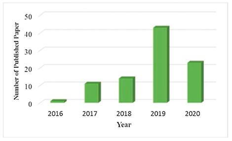
MXenes, a new type of two-dimensional nanomaterial, was successfully prepared by the Naguib research group in 2011 by selectively etching away the A layer from the MAX phase [7]. The MAX phase is a layered ternary carbide and nitride with the general formula Mn+1AXn, where M is an early transition metal (such as Sc, Ti, Zr, Hf, V, Nb, Ta, Cr, Mo), and A is the XIII and XIV elements, X is C or N. 2D MXene is composed of transition metal carbides, carbonitrides and nitrides, and its general formula is Mn+1XnTx (n = 1~3), where Tx represents the surface termination functional group (hydroxyl, oxygen or fluorine) [8, 9]. In recent years, MXene has been extensively studied in energy storage [10-12], water desalination [13], catalysis [14], electromagnetic interference shielding [1], conductive films [15] and many other fields. MXenes has great potential in the field of electromagnetic interference (EMI) shielding because it possess all the fundamental characteristics required for efficient EMI shielding material, including excellent electrical conductivity, light weight, large specific surface area, and most importantly, ease of processability [9]. Since the first report on the outstanding EMI shielding of 2D Ti3C2Tx was published in 2016, the research on the electromagnetic shielding of MXene has registered a blowout type growth (Fig. 1). Herein, we reviewed the synthetic strategies, structural properties and research progress of electromagnetic interference (EMI) shielding of MXene. Based on the research status, we proposed the perspective and outlook about the future development of MXene.

|
Download:
|
| Fig. 1. The number of published papers from Web of Science (Search time: April, 2020) with topics "MXene" and "Electromagnetic shielding" from 2016 to 2020. | |
MXenes reported to date are synthesized by many methods, including top-down etching-assisted exfoliation [7] and bottom-up synthesis (chemical vapor deposition) [16], epitaxial growth [17]. Although there are many ways to prepare MXene, wet-chemical etching in hydrofluoric acid (HF) or HF-containing or HF-forming etchants is nowadays the main method, which add surface functionalities such as –O, –F or –OH, represented by Tx in this formula as Mn+1XnTx. In this section we mainly discuss the recently-reported wet-chemical etching for synthesis MXene including HF etching, in situ HF etching, bifluoride-based etching and fluoride-based salt etching.
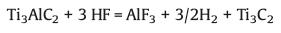
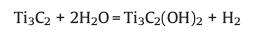
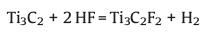
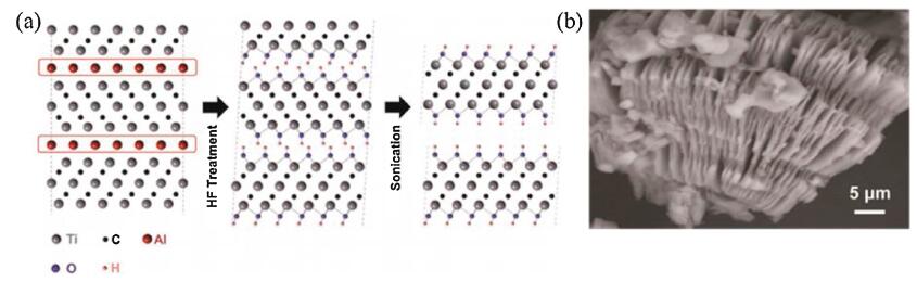
2.1. HF etchingUnlike other 2D materials (such as graphene and black phosphorus), due to the strong metal bond between the "M" and "A" elements, it is difficult to separate the MAX layer by the traditional mechanical exfoliation method [7]. It is fortunate that the M-A metal bond is relatively weak compared to the M-X covalent bond, MXene can be obtained by selectively etching the A element in MAX with hydrofluoric acid (HF) or fluoride-containing etchant. In 2011 [7], Gogotsi and co-workers firstly prepared the Ti3C2Tx MXene with accordion-like layered structure through HF etching (Fig. 2). During the selective etching process, the following simplified reaction occurs:
|
(1) |
|
(2) |
|
(3) |

|
Download:
|
| Fig. 2. (a) Schematic of exfoliation process for Ti3AlC2 by HF etching and (b) SEM image of Ti3C2Tx after HF etching. Reproduced with permission [7]. Copyright 2019, Wiley. | |
Reaction 1 is essential, when reaction 1 takes place, Al atoms in the MAX phase are removed from between the layers to form Ti3C2. The exfoliated 2D Ti3C2 layers possess two exposed Ti atoms, which are highly reactive and easily react with water (reaction 2) or HF (reaction 3) of the reaction medium to form compounds with -OH or -F. It is worth noting that although reactions 2 and 3 are displayed independently, in fact they often occur simultaneously [7]. And the O-terminated MXene is originated from two -OH groups (-OH + -OH → -O + H2O) [18, 19].
Subsequently, the HF etching method has been extended to the synthesis of many other new kinds of MXenes, such as Ti2C, V2C, and Nb2C [20, 21]. As revealed, the etching conditions of MXene are directly related to its precursor MAX phase. In general, the larger the value of n in Mn+1XnTx, the more severe the etching conditions, which means longer etching time, higher reaction temperature and greater concentration of HF [22]. This is mainly because M with a large number of valence electrons usually has a higher metal M—A bond strength [23], so stronger etching conditions are required. For Mn+1XnTx with the same n value, the larger the atomic number of M, the more severe the etching conditions required [21]. This also can be ascribed to the stronger M—A bonding: the larger the atomic number of M, the stronger the bond energy of M—A. In addition, the morphology, particle size, surface termination groups, defect concentration and yield of the same kind of MXene are also related to the etching conditions [24]. Therefore, the etching conditions need to be flexibly adjusted according to the etched object and the actual application.
The multilayer MXene prepared by HF etching has strong interlayer interaction, and it is difficult to obtain single or few layer MXene nanosheets by simple mechanical peeling. Inserting an intercalating agent between multiple layers of MXene and then mechanically peeling is currently the main method to obtain a single or few layers of MXene. Mashtalir et al. [25] inserted dimethyl sulfoxide (DMSO) between the multilayer Ti3C2 nanosheets obtained by HF etching, and then sonicated in water to obtain MXene nanosheets with few or single layers. In addition to DMSO, tetrabutylammonium hydroxide (TBAOH) [26], tetrapropylammonium hydroxide (TPAOH) [27] and isopropylamine (iPrA) [28] are also commonly used intercalating agents.
The HF etching method is currently the most widely used method for synthesizing MXene. Although the HF etching is a simple and easy method to expand production of MXene, the use of HF is also very risky. Therefore, it is extremely important to understand the risk assessment and safety regulations during the preparation process, which is also the main obstacle to the practical application of the HF etching method.
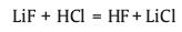
2.2. In-situ HF etchingThe HF etching method is currently the most commonly used method for preparing MXene, but the high concentration of HF is extremely dangerous, so the preparation of MXene by in-situ HF generation from hydrogen fluoride or fluoride salts such as NH4F or LiF is an ideal alternative method. In 2014, Ghidiu et al. [11] initially obtained Ti3C2Tx by etching Ti3AlC2 using a mixed solution of LiF and HCl. Wang et al. [29] originally etched Ti3AlC2 in NH4F solution to prepare Ti3C2Tx. When HCl/LiF or NH4F solution is applied, HF can be in situ generated via the following reactions:
|
(4) |
|
(5) |
The in-situ formed HF will further etch the A atoms of MAX via similar reactions (1-3) with less dangerousness. Compared to the HF etching method, the in-situ HF etching not only avoids the directly usage of concentrated HF, but also facilitates Li+ or NH4+ cations pre-intercalation during etching, which further increases the interlayer spacing and weaken the interlayer interactions between MXene layers. This allows multilayered MXene to be more easily delaminated during sonication, obtaining few layer or monolayer of MXene flakes. Further, by increasing the LiF/Ti3AlC2 molar ratio, single/few layer MXenes can be obtained by hand-shaking [30]. It is worth noting that the delamination method of hand-shaking may produce high-quality MXene nanosheets with larger size and less defects.
Halim et al. [31] compared Mo2CTx obtained by treating Mo2Ga2C with HF and LiF-HCl etchant respectively, the results show that the Mo2CTx nanosheets etched by LiF-HCl have fewer defects. Therefore, compared to the HF etching method, in-situ HF etching is a novel, safer and easier approach to prepare high-quality MXenes.
2.3. Molten salt etchingAlthough various MXenes can be obtained by HF etching or in-situ HF etching, such MXenes are mainly transition metal carbides, such as Ti3C2, Ti2C, V2C, Ta4C3 and Nb2C. According to the first-principles computations, the cohesive energy of Ti—N bonds is lower than that of Ti—C bonds, so the structure of Tin+1Nn is relatively unstable and it is easy to dissolve in HF solution. On the other hand, the formation energy of Ti—N bond is much higher than that of Ti—C bond, indicating that more energy is required to etch Al element from Tin+1AlNn phase. Therefore, it is impractical to prepare nitride MXene by etching its precursor MAX with a fluorine-containing solution [32]. In 2016, Urbankowski et al. [33] successfully used a molten fluoride salt (such as KF, LiF and NaF) to etch Al from Ti4AlN3 precursor at 550 ℃ in argon atmosphere to synthesis the first nitride MXene Ti4N3. Furthermore, the delamination was successfully achieved after intercalation with TBAOH (Fig. 3).

|
Download:
|
| Fig. 3. Schematic illustration of the synthesis of Ti4N3Tx. Reproduced with permission [33]. Copyright 2017, Royal Society of Chemistry. | |
Although the application of molten-salt etching in the preparation of Ti4N3 is efficient, utilizing this approach in the synthesis of new MXenes needs further investigations.
2.4. Fluoride-free etchingThe MXenes obtained by traditional aqueous fluorine-containing acidic solution exist a large number of F-terminal groups, which impairs the electrochemical performance of the material to some extent. In 2018, Li et al. [34] developed an hydrothermal alkali-assisted etching technique to prepare fluorine-free Ti3C2Tx (T= -OH, -O) with high purity. In this process, the control of temperature (T) and alkali concentration (C) is crucial. Only at the proper temperature (T) and alkali concentration (C), the hindrance of the oxides and hydroxides of Al generated from the reaction can be overcome. Since there is no fluorine termination, the gravimetric gravity of Ti3C2 etched by alkali is about 214% higher than HF-etched Ti3C2 (28% higher than HCl/LiF-etched Ti3C2).
Although the reaction conditions of fluoride-free etching are somewhat harsh, it does make a huge contribution to the preparation of fluorine-free MXene, and it deserves further research.
2.5. Lewis acidic molten salts etchingAt present, MXenes are prepared by selective etching of the A-layer in MAX phases through aqueous solutions containing fluoride ions, such as HF [7], LiF/HCl mixture [11], fluoride salt [33]. Therefore, MXenes are now mainly derived from Al-containing MAX phase precursors due to the high reactivity of Al with fluoride-based aqueous solutions. On the other hand, the MAX phase precursors are limited to the traditional A-site elements from group 13-16, the A-site elements of late transition metal (such as Fe, Ni, Zn and Pt) are difficult to synthesize. Therefore, the synthesis of MXenes face two main challenges: (1) Searching for a green, safe and fluorine-free synthetic route to prepare MXenes; (2) Exploring the MAX phase where the A-site is an unconventional element, and establish a broader range of MAX-phase precursors.
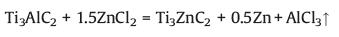
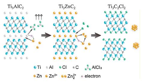
In 2019, Li et al. [35] synthesized a variety of novel MAX phases (Ti3ZnC2, Ti2ZnC, Ti2ZnN and V2ZnC) and MXenes (Ti3C2Cl2 and Ti2CCl2) by elemental replacement in the A atomic plane of traditional MAX phases in ZnCl2 Lewis acidic molten salt (Fig. 4). Taking Ti3ZnCl2 as an example, the formation follows a two-step reaction: (1) the formation of Ti3ZnC2 in an initial stage and (2) the further etching of Ti3ZnC2 in excess ZnCl2 melt to form Ti3C2Cl2. The formation mechanism can be stated as the following simplified reactions:
|
(6) |
|
(7) |

|
Download:
|
| Fig. 4. Schematic illustration of the synthesis of Ti3C2Cl2. Reproduced with permission [35]. Copyright 2019, American Chemical Society. | |
As we all know, ZnCl2 will be ionized to Zn2+ and ZnCl42− in its molten state, and the unsaturated Zn2+ act as the Lewis acids which is a strong acceptor of Cl− and elecrons. According to reaction (6), in this acidic environment, the weakly bonded Al atoms in Ti3AlC2 can be easily converted to Al3+ by a redox reaction, then the in-situ reduced Zn atoms intercalate into the Ti3C2 layers to form Ti3ZnC2. Reaction (7) explain the weakly bonded Zn atoms in Ti3ZnC2 were easily extracted and the Cl− anions spontaneously bonded with the specific site in between Ti3C2 layers to form a more stable phase of Ti3C2Cl2. The formation mechanism of Ti3C2Cl2 is similar to that of chemical etching of Ti3AlC2 in HF solution [7], in which Zn2+ and Cl− act as H+ and F−, respectively.
In 2020, Li et al. [36] successfully extended this etching strategy to a variety of Lewis acid chloride molten salts (CdCl2, FeCl2, CoCl2, CuCl2, AgCl and NiCl2) and broader MAX phase precursor (Ti2CTx, Ti3C2Tx, Ti3CNTx, Nb2CTx, Ta2CTx, Ti2CTx and Ti3C2Tx). More meaningfully, by constructing the Gibbs free energy mapping of the redox potentials/displacement reaction of cations and element A in a high-temperature molten salt environment, a general strategy for the synthesis of 2D MXene by etching the MAX phase with Lewis acid molten salt is proposed.
The lewis acidic molten salts etching method is different from the mainstream strategy of chemical solution etching (such as the widely used HF acid), which greatly improves the chemical safety of the experimental process and reduces the difficulty and cost of waste liquid disposal. Meantime, this novel etching method expands the range of MAX-phase precursors that can be used to prepare new MXenes, and provides unprecedented opportunities for tailoring the surface chemistry and properties of MXene materials.
2.6. Electrochemical etchingSince the traditional fluorine-containing etchant is a hazardous poison with the potential for causing systemic toxicity in human body and fatality, a safe, efficient and low-cost method for MXenes synthesis is nesscerry and imperative. Electrochemical exfoliation of layered materials is a very promising method and has been widely used for the exfoliation of two-dimensional materials such as graphene [37, 38], phosphorene [39], transition Metal Dichalcogenides (TMDs) [40]. Hence, the preparation of MXene by electrochemical exfoliation is very worth exploring.
Sun et al. [41] firstly demonstrated that Ti2CTx MXene can be obtained via electrochemical etching in a three-electrode cell. In this three-electrode system, a homemade porous Ti2AlC, diluted HCl aqueous solution and a Pt foil act as working electrode, electrolyte and counterelectrode, respectively. When a low voltage of +0.6 V was applied for 5 days, Ti2CTx was successfully obtained and confirmed by XRD and SEM. However, the etching reaction took place only at the outer surfaces of the electrode, due to the carbon derived carbide (CDCs) prevent the further etching process.
To overcome this issue, in 2018, Yang et al. [42] demonstrated an efficient electrochemical etching method based on the anodic corrosion of titanium aluminium carbide (Ti3AlC2) in a binary aqueous electrolyte containing NH4Cl and tetramethylammonium hydroxide (TMAOH) (Fig. 5). In this etching process, chloride ions enable rapid etching of Al atom and break the TiAl bonds (Ti3AlC2 −3e− +3 Cl− = Ti3C2 + AlCl3). At the same time, the spontaneous intercalation of ammonium hydroxide opens the boundaries of the etched material, which plays a key role in promoting the complete etching under the surface of elctrode. Under a low potential of +5 V, the Ti3C2Tx (T=O and OH) sheets with large size (up to 18.6 μm in diameter) and with high yield (over 90%) of single and bilayers can be obtained within 5 h. The production rate of 0.6 g/h by the current electrochemical etching method is grater than those from the traditional wet-chemical ways (0.04 g/h). In 2019, Pang et al. [43] extended this electrochemical etching strategy to produce other MXenes (such as Ti2CTx, Cr2CTx and V2CTx) by a thermo-assisted electrochemical route. Hence, this electrochemical etching method has been proven to synthesize a variety of MXene materials.

|
Download:
|
| Fig. 5. Schematic of the etching and delamination process. Reproduced with permission [42]. Copyright 2018, Wiley. | |
Compared with the traditional chemical etching method such as HF etching, this electrochemical etching method does not require any dangerous fluoride-containing agents or harsh etching conditions, and has the advantages of high efficiency and high yield, therefore it is promising for the practical production of MXene materials.
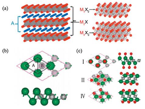
3. Structure and property of MXenes 3.1. The model of MXenes structureProperty is subject to structure, in order to fully understand the property of MXene, it is necessary to explore its atomic structure in detail. MAX phases are layered hexagonal with P63/mmc symmetry, where the M layers are nearly closed packed, and the X atoms fill the octahedral sites [23, 44]. In other words, the crystal structure of MAX phases can be described as layers of edge shared M6X octahedrons intercalated with pure A-group element layers. Depending on the n value, the thickness of the Mn+1Xn changes; if n = 1, then the layer consists of a single block of octahedra, if n = 2, two blocks, and if n = 3, three blocks of octahedra (Fig. 6a). The strong M—X bond has a mixed covalent/metallic/ionic character, whereas the M—A bond is metallic. Therefore, by taking advantage of the differences in character and relative strengths of the M—A compared with the M—X bonds, the A layers can be selectively etched by chemical means without disrupting the M—X bonds [45, 46]. Similar to their MAX precursors, MXenes form hexagonal lattices with the same symmetry. Taking the thinnest MXene systems as an example, Khazaei et al. [47] constructed an appropriate models for 2D MXene systems by removing the "A" element from the bulk MAX phases. An M2X system consists of trilayer sheets with a hexagonallike unit cell, where the X (C or N) layer is sandwiched between the two "M" transition metal layers. On the M2X surface, there are two types of hollow sites, as shown in Fig. 6b: the hollow site A, where no "X" atom is available under the transition metal; and the hollow site B, which is provided with "X" atom.

|
Download:
|
| Fig. 6. (a) Schematics of the M2AX crystal structure and M3X2 and M4X3 layers. Reproduced with permission [23]. Copyright 2015, American Chemical Society. (b) Top and side views of the obtained 2D M2X layer [47]. Copyright 2013, American Chemical Society. (c) Top and side views of models of the functionalized MXene systems [47]. Copyright 2013, American Chemical Society. | |
Since the coordination number of a transition metal ion is often six, it is natural to assume that the transition metals in MXenes make six chemical bonds with the neighboring X atoms and the attached chemical groups on the surfaces, resulting in the formation of M2XF2, M2X(OH)2 and M2XO2 [47]. Therefore, depending on the relative positions of the connected end groups and metal atoms, there may be four configurations for the chemical termination of the M2X system: for type I, two functional groups located on the top of the two transition metals; for type II, two functional groups on top of the hollow sites A; for type III, one functional group located on the top of the hollow site A and the other functional group locates on the top of a hollow site; and type IV has two functional groups located on the top of hollow sites B. Among the four types, type 1 is energetically less stable than any of the other three considered models. In many cases, most MXenes tend to be arranged in a type II-IV.
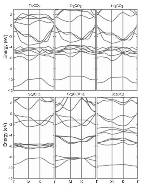
3.2. Electronic propertiesThe electronic properties of MXene, especially its adjustability, has attracted special attention in both theoretical research and practical applications [48-50]. Many theoretical calculations have proved that ideal pristine MXenes are metallic with a substantial electron density near the Fermi level. For example, Gogotsi et al. [7] used DFT calculations to pointed out that pristine Ti3C2 has metallic characteristic when he firstly prepared the Ti3C2Tx MXene. Lashgari et al. [51] demonstrated that all the titanium carbide/nitrides (Ti2C, Ti2N, Ti3C2 and Ti3N2) have metallic properties, since the valance and conduction bands have overlapped at the Fermi level. However, interestingly, some experimental results show that MXenes turn into semiconductors by surface functionalization. As an example, Khazaei et al. [47] conducted a calculation study on the electronic characteristics of M2X-type MXene (Fig. 7). The results show that Sc2CX2 (X = F, OH and O), Ti2CO2, Zr2CO2, Hf2CO2 are semiconducting. The energy gaps of Ti2CO2, Zr2CO2 and Hf2CO2 are 1.03, 0.45 and 1.8 eV, respectivity. From the calculated band structures, it is inferred that Sc2C(OH)2 has a direct band gap and that other semiconductors have indirect band gaps. This is because Ti, Zr and Hf are in the same group in the periodic table with the same number of electrons in their outer shells [47]. Therefore, the corresponding MXene systems exhibit similar metallic to semiconducting behaviors near the fermi energy upon the same type of functionalization.

|
Download:
|
| Fig. 7. Band structure of semiconducting MXene systems. The Fermi energy is at zero. Reproduced with permission [47]. Copyright 2013, Wiley. | |
It is also revealed that the electronic properties of MXenes are also influenced by the type and position of surface functional groups. Zhang et al. [52] conducted a computational study of the electronic properties of Sc2C MXene and its functionalized derivatives. The results revealing that the bare Sc2C layers are metallic. The electronic properties of the most stable configurations of hydrogenated and oxygenated forms are indirect-band-gap semiconductors while the most stable configuration of hydroxylated forms is a direct-band-gap semiconductor. In addition, it is predicted that the O group might differ from F and OH. This is because both F and OH groups can receive only one electron from the surface, but the O group demands two electrons from the surface to be stabilized at its adsorption position.
Currently, in practical applications, the incomparable electrical conductivity of MXenes (especially Ti3C2Tx) is the most crucial factors for continued enthusiasm for the study of MXenes. Gogotsi group [53] obtained Ti3C2Tx films through vacuum-assisted filtration with a conductivity of approximately 2400 S/cm, which is several times more conductive than graphene. Lipatov et al. [54] prepared a Ti3C2Tx-based field-effect transistor (FET) with a conductivity of 4600 ± 1100 S/cm. Naguib et al. [8] prepared the MXene (Ti3C2, Ti2C, TiNbC, Ti3CN and Ta4C3) free-standing thin discs through cold pressing. The resistivities of those discs were 0.005−0.068 Ω/m, these values are comparable to multilayer graphene reported by Li et al. [55] and Blake et al. [56]. In addition, the electrical conductivity of MXenes is also influenced by many factors such as surface groups, nanosheet size, intercalation and contact resistance between flakes. Gogotsi group [57] studied the effect of surface terminations and intercalating agents on the conductivity of MXene by in-situ vacuum annealing. The results show that both H2O and TBA+ intercalants increase sample resistance, and TBA+ has more influence than H2O intercalants. This is because the TBA+ is a large ion which can sinificantl increase the electrical resistance. Morover, MXene can be de-functionalization by vacuum annealing, which greatly improves its conductivity. In most cases, the preparation process directly affects the size and defect concentration of MXenes nanosheets, and the MXene with larger size and smaller defects has higher conductivity. For example [31], compared with the MXene prepared by the traditional HF etching method (~1000 S/cm), the conductivity of the MXene film prepared by the milder in-situ HF etching method is as high as 6000 S/cm.
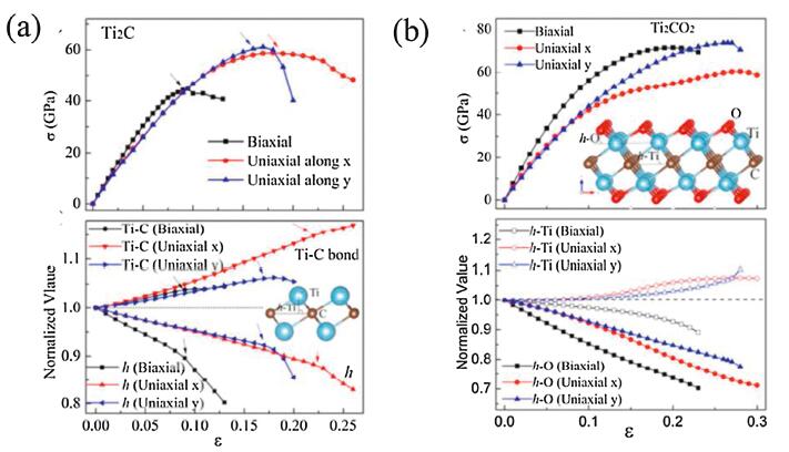
3.3. Mechanical propertiesDue to the presence of strong M—C and/or M—N bonds in MXene, its mechanical properties have also attracted widespread attention. Guo et al. [58] studied the mechanical properties of MXenes take Tin+1Cn (n = 1, 2 and 3) as an example by first principles calculations. The results show that 2D Ti2C can sustain large strains of 9.5%, 18% and 17% under tensions of biaxial and uniaxial along x and y, respectively, which respectively increase to be 20%, 28% and 26.5% for 2D Ti2CO2 by surface functionalizing oxygen, these values is much better than graphene (15% biaxial) (Fig. 8). Furthermore, with n in Tin+1Cn increase, the critical strains do not change much but the Young's modulus decrease slightly. However, for all the Tin+1Cn MXenes, the surface functionalizations could significantly improve their mechanical properties through reducing the Young's modulus and extending the critical strains. This is related to the fracture mechanism of MXene. The failure of 2D Tin+1Cn MXene is due to the significant collapse of the surface atomic layer, while surface functionalization could slow down this collapse, resulting in the improvement of mechanical flexibility.

|
Download:
|
| Fig. 8. Calculated stress-strain curves of 2D Ti2C (a) and (b) Ti2CO2. Reproduced with permission [58]. Copyright 2015, Royal Society of Chemistry. | |
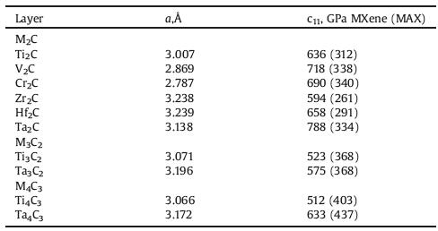
At present, the best way to explain how MXene responds to stress is the elastic constants when they are stretched along the basal planes, i.e., c11. Naguib et al. [59] predicted the c11 values of different Mn+1Cn through density function theory (DFT) calculations. As show in Table 1, with the c11 values of all studied MXenes are lagre than 500 GPa, it appears that these 2D solids are quite stiff, at least when pulled along the basal planes. In addition, the Mn+1Cn layers would be higher than in their parent MAX phases. For the M2AX phases, the c11 values of the MAX phases are roughly 40% lower than those of the corresponding MXenes; for the M3AX2 and M4AX3 phases, the reduction is closer to 70%. On the other hand, the c11 values of MXenes are all signifificantly lower than those for single-layer graphene. However, based on the thickness alone, the bending rigidities of the MXenes are probably orders of magnitude higher than that for graphene, and the MXene mechanical properties should thus be significantly better than those of multilayer graphene of comparable thickness.
|
|
Table 1 Summary of the c11 value of 2D layers calculated herein. Reproduced with permission [59]. Copyright 2012, Cambridge University Press. |
Although theoretical research shows that single-layer MXene has excellent mechanical properties, experimental mechanical testing has only been conducted for MXene films and not for single-layer MXenes. The Ti3C2Tx film prepared by vacuum-sssisted filtration (VAF) can be folded into any shape without damage, which shows the good flexibility of Ti3C2Tx [53]. Interestingly, a cylinder with 4−5 μm thick Ti3C2 film can support 4000 times its own weight. Although MXene has excellent mechanical properties, it can be composited with various polymers to further improve its mechanical properties to meet the needs of various Besides, their mechanical properties can be composited with various polymers to further improve its mechanical properties to meet the needs of various applications [60, 61]. Cao et al. [61] reported that the Ti3C2Tx/CNF composite paper show a high tensile strength (up to 135.4 MPa) and fracture strain (up to 16.7%), as well as excellent folding endurance (up to 14,260 times). Furthermore, Ling et al. [53] reported that Ti3C2 paper roll with 10 wt% PVA could sustain ~15,000 times of its own weight. Although MXene has excellent mechanical properties, it can be composited with various polymers to further improve its mechanical properties to meet the needs of various applications.
3.4. OthersIn addition to the unique electronic and mechanical properties of MXenes, its dispersibility, optical and magnetic properties, etc. have also received more and more research.
Unlike graphene, MXene has fairly great solubility in water, which greatly promotes its processability. Futhermore, Maleski et al. [62] systematically studied the dispersibility of Ti3C2Tx in various organic solvents. The results show that the Ti 3C2Tx can be dispersed in many polar organic solvents, and the best dispersions were achieved in N, N-dimethylformamide, N-methyl-2-pyrrolidone, dimethyl sulfoxide, propylene carbonate, and ethanol. This research not only provides new ideas for MXene storage, but also expanding the opportunities for processing techniques, such as mixing MXenes with other nanomaterials or polymers to form composites.
There is little research on the optical performance of MXene, but it is also of great significance. Zhao et al. [63] observed that Ti3C2Tx obtains 77% transmittance in visible light with a wavelength of 550 nm. Futhermore, Zhang et al. [64] studied the optical properties of the original and functionalized Ti2C and Ti3C2 with F, OH and O. It is shown that, in the range of infrared to ultraviolet light including visible light, the in-plane absorption coefficients are lower for the F and OH functionalized MXenes than the bare and O functionalized ones.
In addition, many of the pristine MXenes are intrinsically magnetic. Gao et al. [65] demonstrated using first-principles calculations that monolayers Ti2C and Ti2N exhibit nearly half-metallic ferromagnetism with the magnetic moments of 1.91 and 1.00 μB per formula unit, respectively. This will stimulate further studies on possible spintronic applications for new two-dimensional materials of MXenes.
4. EMI shielding mechanismCurrently, some likely mechanisms explain the interaction between incident EM radiation and shield materials. In general, a commonly mechanism can be explained as follows: when an EM wave strike the surface of shield material, a portion of the EM waves are immediately reflected due to an impedance mismatch between the shield and air. The remaining waves is absorbed and dissipated as heat energy within the shield owing to attenuation or transmission.
The protection of a shield against the incident EM waves is defined as electromagnetic interference shielding, its shielding efficiency is represented by EMI shielding effectiveness (EMI SE). The attenuation of electromagnetic radiation is mainly achieved through reflection, absorption and multiple reflection mechanisms [66]. Therefore, the total EMI SE is the sum of EMI SE caused by these three mechanisms, as is expressed in Eq. 8.
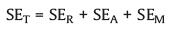
|
(8) |
where SER, SEA and SEM represent the attenuation of EM waves achieved by reflection, absorption and multiple reflection, respectivly.
4.1. Reflection loss (SER)Reflection is a primary EMI shielding mechanism caused by the interface or surface between the two propagation media (e.g., air and the shield) with different impedances or refractive indexes. To reflect electromagnetic waves through the shield material, the shielding surface must have movable charge carriers that interact with the electromagnetic field in the radiation [67]. For a highly conductive shield materials, the simplified version of Fresnel's equation as follows can quantify the magnitude of reflection loss [66]:
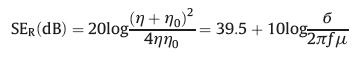
|
(9) |
where η and η0 are the impedances of the shield material and air, respectively, б and μ are the electrical conductivity and the magnetic permeability of the shield material, respectively, and f is the frequency of the incident EM waves. It is obvious from Eq. 9 that the SER increases as the conductivity increases, so the high conductivity of shield materials is necessary to achieve strong SER. However, the SER is not only related to the conductivity of the shielding material, but also to permeability. In addition, the contribution of reflection loss is greater under low-frequency of electromagnetic waves.
4.2. Absorption loss (SEA)A secondary mechanism of EMI shielding is usually absorption loss [67]. The strength or amplitude (E) of the EM wave is exponentially diminished (E = E0e−α) in a shield of thickness of d, where α is an attenuation constant. The value of α can be expressed as a function of ω, μ, б and ε of the shield as Eq. 10.
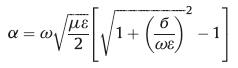
|
(10) |
where ω is angular frequency (2πf) and ε is dielectric permittivity.
Therefore, a high absorption loss needs to meet the following conditions: high electrical conductivity which can cause ohmic loss due to the interaction between the high electron density and incident EM waves; large dielectric permittivity for dielectric loss, which is due to the formation of multiple micro- and nano-capacitors; and large magnetic permeability for magnetic loss, which is associated with magnetic hysteresis loss and eddy current loss. All absorbed electromagnetic waves are eventually dissipate in the form of heat energy.
It is worth noting that the absorption loss is a function of б/μ, and reflection loss is a function of бμ. Therefore, shield with high electrical conductivity tend to reflect electromagnetic waves, while high magnetic permeability tend to absorb electromagnetic waves. Futhermore, the SER decreases with increasing frequency of EM waves, while the SEA increases with increasing frequency.
4.3. Multiple reflections (SEM)Multiple reflection refers to the reflection of electromagnetic waves at various surfaces or interfaces in the shielding material [67]. SEM extends the propagation path length of an EM wave before transmission and provides a higher chance of interaction between the shield and EM radiation, resulting in increased attenuation by absorption. This mechanism requires a large specific surface area or interface area in the shield. It is worth noting that the loss due to multiple reflections can be neglected when the distance between the reflecting surfaces or interfaces is larger compared to the skin depth.
In order to obtain better shielding effect, increasing the specific surface area and introducing more interface areas of the shield is an effective method. For example, shield with porous or foam structure has a larger specific surface area, while the layer-by-layer morphology and segregated structure can provide more interface area.
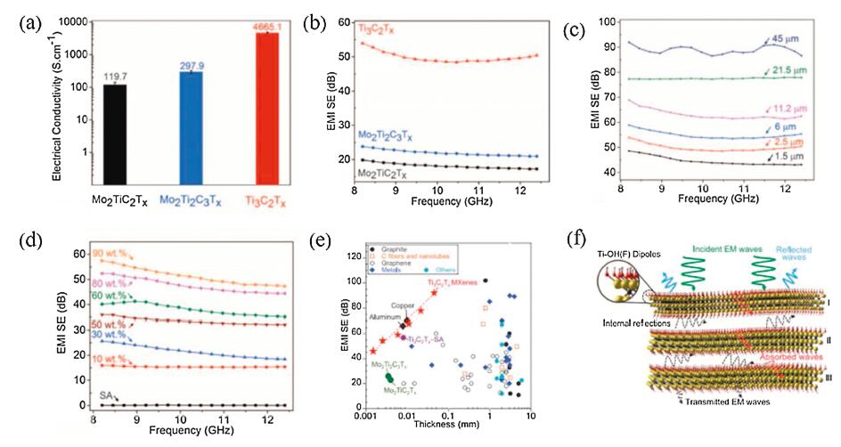
5. MXenes-based materials for EMI shielding 5.1. MXene film 5.1.1. Laminar MXene filmSince the unique feature of ultrathin flakes, MXene can be easily assembled to form laminar film through various methods such as vacuum assisted filtration (VAF). In 2016, Shahzad et al. [1] firstly prepared three different types of laminar MXene film (Ti3C2Tx, Mo2TiC2Tx, and Mo2Ti2C3Tx) and MXene-polymer (Ti3C2Tx-SA) composite film through vacuum assisted filtration starting from colloidal solutions of pure MXenes or its composites, and then studied their electromagnetic shielding performance. Compared with Mo2TiC2Tx and Mo2Ti2C3Tx, Ti3C2Tx exhibited the largest EMI SE value due to its high conductivity (Figs. 9a and b). This results demonstrated that electrical conductivity is a crucial factor in shield. The Ti3C2Tx (45 μm) and Ti3C2Tx-SA film (8 μm) exhibited an highest EMI SE value of 92 dB and 57 dB, respectively (Figs. 9c and d). Compared with pure Ti3C2Tx film, the obtained Ti3C2Tx-SA film has the advantages of excellent mechanical properties, environmental stability and light weight. A 90 wt% Ti3C2Tx-SA composite film (9 μm) exhibited an excellent absolute shielding effectiveness (SSE/t) value of 30,830 dB cm2/g which is several times higher than those of the other materials studied thus far (Fig. 9e). In addition, the mechanism of EMI shielding has been proposed to illustrate the excellent EMI SE value of MXene (Fig. 9f): Firstly, when EMWs strike the surface of MXene film, some EM waves are immediately reflected because of abundant free electrons at the surface of the highly conductive MXene; then the remaining waves go through the MXene lattice structure and interact with the high electron density of MXene, resulting in an ohmic losses of the EMWs; finally, The surviving EMWs that pass through the first layer can be reflected back and forth between the layers (I, II, III and so on) until completely absorbed in the structure. Therefore, the outstanding EMI shielding performance is attributed to the high electrical conductivity and the laminated structure of MXene film.

|
Download:
|
| Fig. 9. (a) Electrical conductivity of Mo2TiC2Tx, Mo2Ti2C3Tx and Ti3C2Tx. (b) EMI SE of Mo2TiC2Tx, Mo2Ti2C3Tx, Ti3C2Tx at a thickness of ~2.5 μm. (c) EMI SE of Ti3C2Tx at different thicknesses. (d) EMI SE of Ti3C2Tx-SA composites at a thickness of 8μm to 9 μm. (e) EMI SE versus thickness of different materials. (f) Proposed EMI shielding mechanism. Reproduced with permission [1]. Copyright 2016, AAAS/Science. | |
Although the laminar MXene film exhibited a superior EMI shielding effectiveness due to its excellent electrical conductivity and the laminar structure, weak mechanical properties and poor oxidation resistance will limit its practical application. So in the follow-up research, the development of strong and tough MXenes composites has grown in popularity.
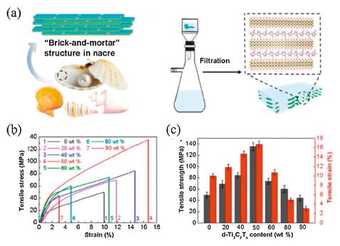
Cao et al. [61] fabricated a Ti3C2Tx-cellulose nanofiber (MXene-CNF) composite film with nacre-like structure by a simple vacuum-assisted filtration method, and the EMI shielding and mechanical properties of the composite film has been studied (Fig. 10a). CNF with a one-dimensional structure cannot only play a reinforcing role, but also lead to less insulating contacts between 2D conductive MXene nanosheets. The composite film exhibited a high conductivity (739.4 S/m) and excellent EMI shielding efficiency (2647 dB cm2/g) at a thickness of 47 μm. The composite film shows a outstanding mechanical properties with a tensile strength of 154 MPa and strain of 16.7% (Figs. 10b and c). In addition, it can also sustain up to 14,260 folding without damage. The enhanced mechanical properties are mainly due to the following three factors: hydrogen bonds, flexible CNFs, and nacre-like structure. Hydrogen bonds between MXene and CNFs allow the composite to endure more stress under tension; Flexible CNFs provide additional friction energy dissipation between adjacent MXene nanosheets to resist the sliding effect and toughen the MXene-CNF composite paper; In the nacre-like structure or"brick-and-mortar" structure, MXene nanosheets function as the "brick" and offer the frame for the MXene/CNFs film, and the 1D CNFs act as the "mortar", which not only connect the adjacent MXene nanosheets but also promote the stress transfer and enhance the frictional energy dissipation.

|
Download:
|
| Fig. 10. (a) Schematic illustration of the "brick-and-mortar" structure in nacre (left) and the preparation of the MXene/CNF composite film via a vacuum filtration method (right). (b) Tensile stress − strain curves of the d-Ti3C2Tx/CNF composite paper with different Ti3C2Tx contents. (c) Tensile strengths and strains of the MXene/CNF composite film with different MXene contents. Reproduced with permission [61]. Copyright 2018, American Chemical Society. | |
In addition to 1D CNF, Xie et al. [68] also prepared Ti3C2Tx/aramid nanofiber (MXene/ANF) film via vacuum-assisted filtration method. The obtained MXene/ANF film showed a excellent mechanical properties with a tensile strength of 197 MPa and fracture strain of 9.8%. The conductivity of the composite film increases significantly with the increase of MXene, and reached a maximum value of 628.872 S/cm at 10% ANF addition. Furthermore, the MXene/ANF exhibited excellent EMI SE, which was accomplished beyond the commercial standard for EMI shielding materials when the addition of MXnee exceeds 20%. He et al. [69] fabricated a Ti3C2Tx/hydroxyethyl cellulose (MXene/HEC) composite film through vacuum-assisted filtration. The introduction of HEC improved the mechanical properties of the composite film due to the formation of hydrogen bonds between HEC and MXene. The MXene/HEC composite film exhibited 24 dB at 100 μm thick in 8.2–12.4 GHz.
The combination of MXene and polymer (such as SA, CNF) can usually obtain a lightweight MXene film with excellent mechanical properties and flexibility, but the inherent insulation of the polymer will inevitably reduce the conductivity of MXene. Conductive polymers cannot only improve the mechanical properties of MXene, but also greatly retain its high conductivity which is due to the conductive chains between MXene layers create a conductive path to reduce the contact resistance and aid the flow of electrons.
Liu et al. [70] first proposed the scheme of compounding Ti3C2Tx and conductive polymer to obtain an ultra-thin, high-flexibility and pearl-like MXene/PEDOT: PSS composite film with a "brick and mortar" structure (Fig. 11a). In this "brick and mortar" structure, MXenes as inorganic "brick" offer framewor for composite film, and amorphous PEDOT: PSS as organic "mortar", which not only connect the adjacent MXenes nanosheets but also promote the stress transfer and enhance the dissipation of fractured energy. Compared with the pure MXene film, the 3:1 composite film (MXenes to PEDOT: PSS) exhibited the highest tensile strength (30.18 MPa), nearly 5.4 times of that of pure MXene film and the corresponding fracture strain is increase from 0.18% to 1.51% (Fig. 11b). As we all know, the electrical conductivity is of great significance for EMI shielding materials. Compared with pure MXene film (1000 S/cm), the MXene/PEDOT: PSS composite film greatly retain its high conductivity, when MXene to PEDOT: PSS ratio is 7:1, the corresponding electrical conductivity is about 340.5 S/cm (Fig. 11c). Furthemore, the EMI SE value of composite film with 7:1 ration (11.1 μm, 1.94 g/cm3) up to 42.10 dB, which is comparable to pure MXene film (42.48 dB) and but the strength increases by 2.4 times (Fig. 11d). This result further demonstrates that the conductive polymer not only retains the excellent EMI shielding performance of MXene, but also greatly improves its mechanical properties (Fig. 11e).

|
Download:
|
| Fig. 11. (a) Schematic illustration of the MXene/PEDOT: PSS composite film with a "brick-and-mortar" structure. (b) Tensile stress-strain curves, (c) electrical conductivity and thickness and (d) EMI SE of pure MXene film and the composite film. (e) Comparison of the SSE/t as a function of thickness. Reproduced with permission [70]. Copyright 2018, American Chemical Society. | |
In addition to conductive polymer PEDOT: PSS, Zhang et al. [71] prepared a Ti3C2Tx/co-doped polyaniline (MXene/c-PANI) composite by vacuum assisted filtration and the mechanical properties and EMI shielding performance was studied. The electrical conductivity, EMI SE, and tensile strength were significantly enhanced to 24.4 S/cm, 36 dB and 19.9 MPa, which were 81, 2.3 and 7.7 times those of pure c-PANI film (0.3 S/cm, 16 dB and 2.6 MPa), respectively.
5.1.2. Layer-by-layer (LBL) structured MXene filmThe LBL structured film refers to a film with a "-A-B-A-B-A-B-" alternating layer structure, which is based on sequential adsorption of nanometer-thick monolayers of oppositely charged compounds. Many solution-processing techniques (such as solution casting [72], spin coating [73], spray coating [74] and interfacial assembly) can produce LBL structured film. Since the abundant functional groups on the surface of MXene, it can be easily dispersed in aqueous and organic solvents, so it is very suitable for the preparation of structured MXene film.
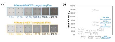
Weng et al. [74] prepared cross-functional semi-transparent Ti3C2Tx-carbon nanotubes (MXenes/CNT) composite film via spin spray layer-by-layer method and studied its EMI shielding performance. The obtained MXene/CNT composite film shows a good transparency which will play an important role in many fields (Fig. 12a). A 300 bilayer composite film with a thickness about 200 nm has an electrical conductivity of 130 S/cm and an absolute EMI SE (SSE/t) of 58,187 dB cm2/g. These values are among the highest reported values for flexible and semi-transparent composite thin films (Fig. 12b). Interestingly, the main shielding mechanism of these as-prepared MXene/CNT composite films is EM wave absorption. This shielding characteristic is closely related to the LbL structure of film, which assembly of two phases with different impedances can cause major internal scattering at the internal interfaces and aids the attenuation of the incident EM radiation.

|
Download:
|
| Fig. 12. (a) MXene/CNT composite films with different bilayers. (b) Comparison of the specific EMI shielding effectiveness of different materials. Reproduced with permission [74]. Copyright 2018, Wiley. | |
Jin et al. [72] prepared PVA/MXene composite film by alternating casting method. In this composite film, the MXene layer provides a continuous network of thermal and electrical conductivity, allowing the PVA substrate to have both EMI shielding and thermal conductivity. The PVA/MXene multilayer film (19.5 wt% MXene) with a thickness of 27 μm exhibited a conductivity of 716 S/m, an SE value of 44.4 dB and a specific SE value of 9343 dB cm2/g. This outstanding EMS shielding performance is due to the multilayered LbL structure with alternating conducting and non-conducting layers had mismatched impedance and enhanced the internal scattering and absorption of EM radiation. At the same time, the multilayer film shows an in-plane thermal conductivity of 4.57 W/mK, which is about 23 times that of a pure PVA film.
Zhou et al. [75] fabricated a MXene/CNF composite film with alternating multilayered (LbL) structure via a facile and efficient alternating vacuum filtration approach (Fig. 13a). Compared to both freestanding MXene film and homogeneous CNF/MXene film, this alternating multilayered film exhibited the improved mechanical strength (112.5 MPa) and toughness (2.7 MJ/m3) due to the mechanical frame effect acted by CNF layers. Meanwhile, the obtained LbL MXene/CNF film show a high electrical conductivity of 82–621 S/m, which is more than 41–310 times that of the homogeneous CNF/MXene film (2 S/m). Interestingly, the electrical conductivity of in-plane is about 9 orders higher than the through-plane, this anisotropic electrical conductivity suggests the huge potential in applying in insulation-required EMI shielding (Fig. 13b). More importantly, the LbL MXene/CNF film demonstrated an exceptional EMI shielding effectiveness of ~40 dB in the X-band and K-band and high specific shielding effectiveness up to 7029 dB cm2/g at a thickness of only 35 μm (Fig. 13c). Such excellent EMI shielding effect is not only related to its high electrical conductivity, but more importantly, this LBL structure with conductive and non-conductive layers has an mismatched impedance, thus providing additional "reflection-absorption-zigzag" reflection, which greatly improves the EMI SE (Fig. 13d).

|
Download:
|
| Fig. 13. (a) AVF process to prepare alternating multilayered MXene/CNF film. (b) Electrical conductivity of MXene/CNF film. (c) EMI SE of MXene/CNF film at X- bands. (d) EMI SE of MXene/CNF film at K- bands. (e) Schematic illustration of EMI shielding mechanism of MXene/CNF film. Reproduced with permission [75]. Copyright 2020, American Chemical Society. | |
With the vigorous development of portable electronics and wearable textiles, flexible textiles with conductive and electromagnetic shielding functions have received more and more attention. The combination of conductive filler and fabric cannot only retain the flexibility, stretchability and breathability of the fabric itself, but also give it electrical conductivity, thermal conductivity and EMI shielding functions. The MXene with high conductivity and sufficient functional groups is very suitable for fabricating electrical textiles.
Liu et al. [76] prepared Ti3C2Tx MXene and silver nanowire (AgNW) decorated silk fabrics with superb EMI shielding performances, superhydrophobicity and highly sensitive humidity response via vacuum-assisted LbL spray coating. The composite film has a leaf-like structure with MXene as the conductive lamina and AgNWs as the conductive vein. This multifunctional film exhibits a low sheet resistance of 0.8 Ω/sq, outstanding EMI SE of 54 dB in the X-band at a small thickness of 120 μm, while retaining its satisfactory porosity and permeability.
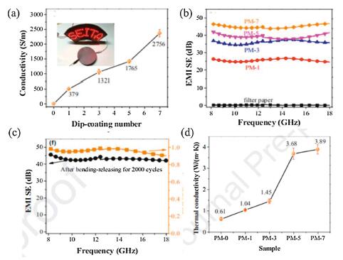
Hu et al. [77] designed and prepared a highly electrically and thermally conductive, bendable and durable MXene/cellulose film via a simple dip-coating method. The commercial cellulose filter paper was selected as substrate, then interconnected MXene endows the composite film with high electrical and thermal conductivity. The obtained composite film exhibits a marvelous electrical conductivity of 2756 S/m at a nanosheet loading of 1.89 vol% due to the intrinsic metallic conductivity of Ti3C2Tx nanosheets and their interconnected network (Fig. 14a). Meanwhile, the MXene/cellulose film can exhibit EMI SE higher than 43 dB in X-band and Ku-band (Fig. 14b). More importantly, the composite film possesses remarkable mechanical stability, preserving over 90% EMI SE retention after 2000 bending-releasing cycles (Fig. 14c). In addition, the composite film also shows an in-plane thermal conductivity of 3.89 W m−1 K−1 (Fig. 14d).

|
Download:
|
| Fig. 14. (a) Electrical conductivity of M-filter as a function of dip-coating cycles. (b) EMI SE of the filter paper and the PDMS-coated M-filter in the X and Ku band. (c) EMI SE of the PM-7 after 2000 bending-releasing cycles and the EMI SE retention. (d) In-plane thermal conductivity of the as-prepared nanocomposite paper. Reproduced with permission [77]. Copyright 2020, American Chemical Society. | |
Zhang et al. [78] prepared a MXene-decorated woven cotton fabrics (M-CF) with an interwoven conductive network via the simple spray-drying coating method. The degree of conductive interconnection of the fabric can be precisely adjusted by adjusting the spray drying cycle and then the conductivity and EMI SE can be adjusted. The MXene-decorated fabrics show an outstanding electrical conductivity of 5 Ω/sq with a low loading of 6 wt% (0.78 mg/cm2) due to the interwoven conductive architecture. Meanwhile, the obatined MXene-decorated fabrics had outstanding EMI shielding performance (up to 36 dB) at very low loading (6 wt%). In addition, the MXene-decorated fabrics also possessed outstanding joule heating and retained the original air permeability and flexibility of fabric.
Ma et al. [79] prepared a flexible, breathable, wearable and stable MXene-decorated air-laid paper with superb folding endurance and the EMI-shielding performance by a simple "dipping and drying" method. The air-laid papers can be covered by the MXene driven by van der Waals forces and hydrogen bonding between MXene nanosheets and cellulose in "dipping and drying" process. The MXene-decorated paper exhibited a high electrical conductivity of 173.0 S/m and a superior EMI shielding efficiency (more than 90% of the EM waves in X-band can be shielded), good mechanical flexibility (more than 9.8 × 10⁴ times can be folded) and breathability.
5.1.4. MXene hybrid filmMXene hybrid film refers to the combination of MXenes with other conductive or magnetic materials to further enhance the EMI shielding effectiveness.
Cao et al. [80] constructed an ultrathin and fexible CNT/MXene/CNF composite film with gradient and sandwich structure via a facile alternating vacuum-assisted fltration and investigated the synergistic effect of conductive CNTs and CNFs for EMI shielding and mechanical properties in MXenes film. The obtained composite film shows outstanding mechanical properties with a tensile strength of 97.9 MPa and a fracture strain of 4.6%. The CNT/MXene/CNF hybrid film with an thickness of 38 μm shows a high electrical conductivity of 2506.6 S/m and EMI SE of 38.4 dB due to the synergistic effect of conductive CNTs-MXene and nonconductive CNFs.
Lightweight and flexible MXene/CNF/silver composite film with a brick-like structure have been prepared for EMI shielding applications [81]. The MXene/CNF/silver composite film was produced through the vacuum filtration method, where using MXene as a reducing agent to obtain silver nanoparticles. The composite film show good electrical conductivity of 588.2 S/m and outstanding EMI SE of about 50.7 dB at a thickness of 46 μm. This EMI shielding performance is much higher than a MXene/CNF film with comparable thickness.
Wang et al. [82] fabricated a flexible and ultrathin PVDF/MXene/Ni composite film and investigated the synergistic effect of MXene and Ni chains for EMI shielding performance. The tensile strength, Young's modulus and toughness of the PVDF/MXene/Ni chain composite films are about 41.9 MPa, 1.18 GPa and 2.9 MJ/m3, respectively. A 0.3 mm thick PVDF/MXene/Ni composite film exhibited an electrical conductivity of 892 S/m and EMI SE of 34.4 dB, which are better than when using MXenes or Ni chains alone at the same loading.
Xiang et al. [83] prepared a lightweight and ultrathin TiO2-Ti3C2Tx/graphene film with EMI shielding by vacuum filtration and pyrolysis. In this process, Ti3C2Tx/graphene film was firstly prepared by vacuum filtration, and then Ti3C2Tx was partially converted into TiO2 through thermal treatment to produce the TiO2-Ti3C2Tx/graphene film. The composite film exhibited a low surface resistance of 7.5 Ω/sq and excellent EMI SE above 27 dB. More importantly, when considering the density and thickness of shielding film, the TiO2-Ti3C2Tx/graphene film shows an astonishing shielding performance with the value of SSE/t of 30291.43 dB cm2/g.
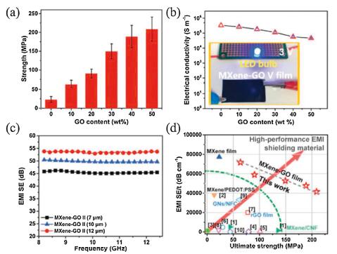
Liu et al. [84] fabricated a GO-reinforced MXene films with high electrical conductivity and exceptional mechanical strength via vacuum-assisted filtration. The obtained MXene/GO film show a outstanding tensile strength of 209 MPa, which is more than about 9 time that of the pure MXene film of 23 MPa (Fig. 15a). Meantime, the composite film shows a high electrical conductivity of 2.64 × 10⁵ S/m, which is comparible to the pure MXene film (Fig. 15b). The excellent electrical conductivity of the MXene/GO film contributed to an outstanding EMI SE of 50.5 dB at a small film thickness of 7 μm (Fig. 15c). In addition, The MXene-GO films are compared with relevant shielding films reported in the literature in terms of specific SE versus strength (Fig. 15d).

|
Download:
|
| Fig. 15. (a) Tensile strength and (b) Electrical conductivities of MXene/GO film with different GO contents; (c) Influences of thickness on EMI SE of MXene-GO film; (d) Comparison of EMI SE/t and strengths of the MXene-GO films with those reported in the literature. Reproduced with permission [84]. Copyright 2019, Wiley. | |
Miao et al. [85] prepared ultrathin, lightweight and flexible AgNWs/NC/MXene composite film via the pressured-extrusion film-forming process. In this scheme, nanocellulose (NC) is firstly dispersed between 2D MXene nanosheets via a hydrogen bonding reactions to form a "brick-and-mortar" network, and then silver nanowires (AgNWs) are intercalated into the network to form a highly interpenetrating 1D/2D integrated conductive network. The obtained composite film exhibited a remarkable conductivity of 30,000 S/m and an outstanding specific EMI SE of 16,724 dB. The tensile stress of AgNWs/NC/MXene composite film is 63.80 MPa, which is more than about 49.5 times than the pure MXene film (1.29 MPa). In addition, after bending 10,000 times at 135 ℃, the conductivity and EMI SE of the composite film still showed good stability.
Liu et al. [86] in order to balance the mechanical strength and electrical conductivity of MXene film, they fabricated a high-performance MXene film by reinforcing the interfacial adhesion among adjacent nanosheets with multivalent aluminum ions (Al3+), which utmost alleviating the damage to the intrinsic electrical conductivity of MXene film. The introduction of Al3+ ions not only enhances the tensile strength of MXene film from 28.7 MPa to 83.2 MPa, and exhibited a high conductivity of 265,600 S/m which is comparable to the pristine MXene film. Thanks to ultra-high conductivity, MXene film shows an excellent EMI SE of 80 dB in the X-band at a small thickness of 39 μm.
5.2. MXenes foamAs we all know, electromagnetic shielding refers to the reflection or absorption of electromagnetic waves by shielding materials. Since reflection of EM radiation generates secondary EM pollution, a great deal of attention has been paid to prepare the shielding material with absorption-dominated feature. In recent years, the foam shielding material with a porous structure has attracted wide attention because it cannot only reduce the density of the shielding material, but more importantly, it can absorb more electromagnetic waves due to impedance matching.
Liu et al. [87] firstly prepared a freestanding, flexible and hydrophobic MXene foam by assembling MXene sheets into films followed by a hydrazine-induced foaming process. Compared with the typical hydrophilic nature of MXene film (water contact angle of 59.5°), MXene foam shows a super hydrophobic surface (water contact angle of 94.0°). The electrical conductivity of MXene foams were 58000–62500 S/m at different thickness, which is lower than that of the MXene film (400,000 S/m). However, it is interesting that the lower conductivity MXene foam exhibits a higher EMI SE of 70 dB compared to the MXene film (53 dB), which is due to the multireflection and scattering of the incident EM waves within the porous structure of the MXene foam.
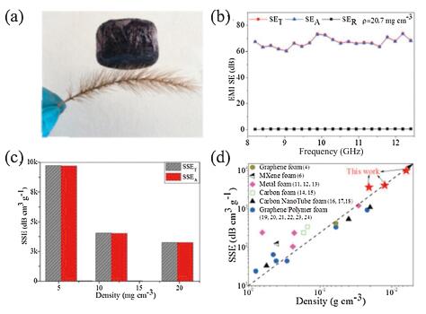
Bian et al. [88] firstly reported an ultralight MXene aerogels without using external supporters through freeze-casting route. The density of the MXene aerogel could be tuned to as low as 4 mg/cm3, which can freely stand on the leaf of a foxtail grass (Fig. 16a). The MXene aerogel exhibited an electrical conductivity of 22 S/cm, this conductive porous structure exhibited an outstanding EMI SE of up to 70 dB and high specific shielding effectiveness of 9904 dB cm3/g. More importantly, such excellent EMI shielding performance is mainly attributed to the absorption loss (SEA), which can be proved by the SER value of less than 1 dB (Figs. 16b and c). The MXene aerogels outperform these existing foam materials in EMI shielding performance in particular EM absorption (Fig. 16d).

|
Download:
|
| Fig. 16. (a) A MXene aerogel (35 cm3) standing on a foxtail grass. (b) EMI SE of total, reflection and absorption of the MXene aerogel. (c) Total EMI SSE (EMI SET) and absorption (SSEA) at 8.2 GHz. (d) Comparison of the SSER and SSET as a function of density for various foam-like materials. Reproduced with permission [88]. Copyright 2019, Royal Society of Chemistry. | |
MXene/PVA hybrid composite foams have been prepared for EMI shielding applications [89]. The composite foams with varying MXene to PVA ratio were produced by a freeze-drying method using ice as a template. The obtained MXene/PVA foam showed an excellent absorption-dominated shielding performance with the SER value of less than 2 dB. Meantime, the obtained foam showed a specific shielding effectiveness reaches up to 5136 dB cm2/g with an ultralow filler content of only 0.15 vol%.
A MXene aerogel with tunable ratio of SER to SEA has been formed using a bidirectional freeze-casting method [90]. The EMI SE of Ti3C2Tx MXene aerogels reached up to 70.5 dB and showed a highest specific SE of 8818.2 dB cm3/g. In addition, the MXene aerogel showed a certain resistance to compression with the maximum stress recovery maintains a stable ratio of about 84.5% after 5 cycles. More importantly, the ratio of SER to SEA varies with the thickness of the aerogel, while the change in SEt is very small. For example, when the Ti3C2Tx with a thickness of 3 mm is compressed to 1 mm, the SER increases from 6.1 dB to 12.9 dB, while the SEA decreases from 62.4 dB to 57.6 dB. This phenomenon is caused by the change in the electrical conductivity and inner pore structure of the aerogel during compression.
Weng et al. [91] prepared a AgNW/MXene composite sponge through a combination of dip-coating and unidirectional freeze-drying methods and investigated its EMI shielding performance. AgNWs were firstly coated on a commercial melamine formaldehyde sponges (MF) to obtain BMF/AgNW, and then MXene is introduced into BMF/AgNW by unidirectional freeze drying to obtain AgNW/MXene sponge.The obtained AgNW/MXene exhibits a higher EMI SE of 52.6 dB with a low density of 49.5 mg/cm3 which is higher than that of the BMF/AgNW due to the synergetic effects of the AgNW and MXene both in conductivity and hierarchical structure.
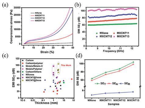
Sambyal et al. [92] prepared MXene/CNT composite aerogel with light weight, good mechanical properties, high electrical conductivity and excellent electromagnetic shielding properties by a bidirectional freezing method. Introducing CNT into MXene aerogel will increase its compression modulus, which is an increase of two orders of magnitude compared to pure MXene aerogel (Fig. 17a). The synergistic effect of the layered and porous structure of the MXene/CNT composite aerogel resulted in an excellent electrical conductivity of 9.43 S/cm and outstanding EMI SE of 103.9 dB, which exhibit the largest EMI SE among the synthesized porous nanomaterials (Figs. 17b and c). In addition, the aerogel exhibited EMI shielding with absorption-dominated feature (Fig. 17d).

|
Download:
|
| Fig. 17. (a) Stress–strain curves and (b) EMI SE of MXene/CNT aerogels. (c) Comparison of EMI shielding performance of MXene/CNF aerogel with other porousmaterials. (d) EMI SET, SEA and SER of MXene/CNF aerogel. Reproduced with permission [92]. Copyright 2019, American Chemical Society. | |
Liang et al. [93] constructed MXene/WPC porous materials with high-temperature carbonized wood-derived porous carbon (WPC) as the skeleton. This porous material can achieve the best EMI SE up to 71.3 dB at a density as low as 0.197 g/cm3. In addition, MXene/WPC porous materials also exhibited good anisotropic compressive strength, excellent thermal insulation and flame retardancy. Wu et al. [94] prepared PDMS-coated SA/MXene aerogels with high conductivity, light weight and compressibility through directional freezing and freeze drying techniques. This composite aerogel has excellent conductivity of 2211 S/m and high EMI SE of 70.5 dB. In addition, the PDMS coating effectively gives the 3D conductive network excellent compressibility and durability. Fan et al. [95] developed a lightweight MXene/graphene aerogel through freeze-drying and reduction heat treatment. The excellenet electrical conductivity of 1250 S/m and porous structure enables MXene/graphene with an excellent EMI SE of 50.7 dB and SSE of 6217 dB cm3/g.
Compared with MXene film, MXene foam with a porous structure has a larger specific surface area and interface area, which will facilitate multiple internal reflections of electromagnetic waves inside the shielding material, resulting in additional attenuation due to absorption. Therefore, MXene foam has great potential in the preparation of absorption-dominated shielding materials.
5.3. MXenes compositesHan et al. [96] mixed the MXene powder before annealing and after annealing with paraffin wax to study the effect of annealing on the electromagnetic shielding performance of MXene. The paraffin wax composite with 50 wt% annealed MXenes showed a minimum reflection loss of −48.4 dB at 11.6 GHz due to the formation of TiO2 nanocrystals and amorphous carbon. However, the EMI SE of annealed MXene (32 dB) is lower than the unannealed MXene (76.1 dB) due to the lower percolation threshold of annealed MXene in paraffin than unannealed MXenes.
Sun et al. [97] fabricated a highly conductive MXene/polystyrene composite through electrostatic assembling of negative MXene nanosheets on positive polystyrene microspheres and compression molding. The obtained MXene/polystyrene exhibited a high conductivity of 1081 S/m due to the highly efficient conducting network. Such high conductivity endows MXene/polystyrene composite with excellent EMI SE of 54 dB with only 1.90 vol% of MXene.
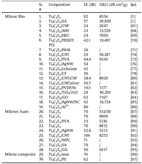
6. Conclusions and perspectivesSince MXene was firstly prepared in 2011, due to its unique physical and chemical properties, it has become a hotspot in the research of two-dimensional materials, and has made important progress in many fields, especially in the EMI shielding field. In this review, we have focused on the synthetic progresses, structure and properties of MXenes, as well as its EMI shielding research progress. Summarized EMI SE and their corresponding absolute shielding effectiveness (SSE/t) have been given in Table 2.
|
|
Table 2 EMI shielding performance of various structural forms based on MXene. |
However, to extensively realize the fundamental and EMI shielding application study about the MXenes, several challenges should be overcome in the future research.
We must consider the limitations in production prior to conducting application-focused research. As far as the synthesis of MXene is concerned, environmentally friendly, cost-effective and scalable production are the research trends. The new strategies such as lewis acidic molten salts etching and electrochemical etching that are expected to replace traditional chemical etching methods are worth exploring harder. Additionally, there are many theoretically predicted MXene species and their performance also need to be experimentally verified. Moreover, since many characteristics of MXene are related to its surface functional groups, it is necessary to make MXene surface terminations with adjustability. Among them, the research of F-free terminated and Cl-terminated MXene should arouse special attention.
For the application of MXenes in EMI shielding field, only a few MXenes (Ti3C2, Ti2C, Mo2TiC2, Mo2Ti2C3 and Ti3CN) have been investigated. Other MXenes should also be explored to better understand the shielding mechanism of MXenes. In addition, although MXenes shows an excellent EMI performance, these materials are highly susceptible to oxidation, which is no doubt that it will reduce the EMI shielding performance. But to date only a few research study the stability of MXene shielding materials in practical applications. Additionally, the exact mechanism of EMI shielding still needs further exploration. Hence, the research of MXenes is still in its infancy, and there is plenty of room for innovation and growth.
Declaration of competing interestThe authors declare that they have no known competing financial interests or personal relationships that could have appeared to influence the work reported in this paper.
| [1] |
F. Shahzad, M. Alhabeb, C.B. Hatter, et al., Science 353 (2016) 1137-1140. DOI:10.1126/science.aag2421 |
| [2] |
Z. Zhou, J. Liu, X. Zhang, et al., Adv. Mater. Interfaces 6 (2019) 1802040. DOI:10.1002/admi.201802040 |
| [3] |
Y. Zhang, Y. Huang, T. Zhang, et al., Adv. Mater. 27 (2015) 2049-2053. DOI:10.1002/adma.201405788 |
| [4] |
P. He, M. Cao, Y. Cai, et al., Carbon 157 (2020) 80-89. DOI:10.1016/j.carbon.2019.10.009 |
| [5] |
X. Huang, B. Dai, Y. Ren, et al., J. Nanomater. 2015 (2015) 2. |
| [6] |
H. Gargama, A.K. Thakur, S.K. Chaturvedi, J. Alloys. Compd. 654 (2016) 209-215. DOI:10.1016/j.jallcom.2015.09.059 |
| [7] |
M. Naguib, M. Kurtoglu, V. Presser, et al., Adv. Mater. 23 (2011) 4248-4253. DOI:10.1002/adma.201102306 |
| [8] |
M. Naguib, O. Mashtalir, J. Carle, et al., ACS Nano 6 (2012) 1322-1331. DOI:10.1021/nn204153h |
| [9] |
B. Anasori, M.R. Lukatskaya, Y. Gogotsi, Nat. Rev. Mater. 2 (2017) 16098. DOI:10.1038/natrevmats.2016.98 |
| [10] |
M.R. Lukatskaya, O. Mashtalir, C.E. Ren, et al., Science 341 (2013) 1502-1505. DOI:10.1126/science.1241488 |
| [11] |
M. Ghidiu, M.R. Lukatskaya, M.Q. Zhao, et al., Nature 516 (2014) 78-81. DOI:10.1038/nature13970 |
| [12] |
X. Liang, A. Garsuch, L.F. Nazar, Angew. Chem. 54 (2015) 3907-3911. DOI:10.1002/anie.201410174 |
| [13] |
C.E. Ren, K.B. Hatzell, M. Alhabeb, et al., J. Phys. Chem. Lett. 6 (2015) 4026-4031. DOI:10.1021/acs.jpclett.5b01895 |
| [14] |
Z.W. Seh, K.D. Fredrickson, B. Anasori, et al., ACS Energy Lett. 1 (2016) 589-594. DOI:10.1021/acsenergylett.6b00247 |
| [15] |
A.D. Dillon, M.J. Ghidiu, A.L. Krick, et al., Adv. Funct. Mater. 26 (2016) 4162-4168. DOI:10.1002/adfm.201600357 |
| [16] |
C. Xu, L. Wang, Z. Liu, et al., Nat. Mater. 14 (2015) 1135-1141. DOI:10.1038/nmat4374 |
| [17] |
K. An, X. Xu, Electrochim. Acta 293 (2019) 348-355. DOI:10.1016/j.electacta.2018.10.050 |
| [18] |
M.A. Hope, A.C. Forse, K.J. Griffith, et al., Phys. Chem. Chem. Phys. 18 (2016) 5099-5102. DOI:10.1039/C6CP00330C |
| [19] |
L.H. Karlsson, J. Birch, J. Halim, et al., Nano Lett. 15 (2015) 4955-4960. DOI:10.1021/acs.nanolett.5b00737 |
| [20] |
B. Ahmed, D.H. Anjum, M.N. Hedhili, et al., Nanoscale 8 (2016) 7580-7587. DOI:10.1039/C6NR00002A |
| [21] |
M. Naguib, J. Halim, J. Lu, et al., J. Am. Chem. Soc. 135 (2013) 15966-15969. DOI:10.1021/ja405735d |
| [22] |
B. Anasori, Y. Xie, M. Beidaghi, et al., ACS Nano 9 (2015) 9507-9516. DOI:10.1021/acsnano.5b03591 |
| [23] |
M. Naguib, Y. Gogotsi, Acc. Chem. Res. 48 (2015) 128-135. DOI:10.1021/ar500346b |
| [24] |
M. Alhabeb, K. Maleski, B. Anasori, et al., Chem. Mater. 29 (2017) 7633-7644. DOI:10.1021/acs.chemmater.7b02847 |
| [25] |
O. Mashtalir, M. Naguib, V.N. Mochalin, et al., Nat. Commun. 4 (2013) 1716. DOI:10.1038/ncomms2664 |
| [26] |
M. Naguib, R.R. Unocic, B.L. Armstrong, et al., Dalton Trans. 44 (2015) 9353-9358. DOI:10.1039/C5DT01247C |
| [27] |
H. Lin, S. Gao, C. Dai, et al., J. Am. Chem. Soc. 139 (2017) 16235-16247. DOI:10.1021/jacs.7b07818 |
| [28] |
O. Mashtalir, M.R. Lukatskaya, M.Q. Zhao, et al., Adv. Mater. 27 (2015) 3501-3506. DOI:10.1002/adma.201500604 |
| [29] |
L. Wang, H. Zhang, B. Wang, et al., Electron. Mater. Lett. 12 (2016) 702-710. DOI:10.1007/s13391-016-6088-z |
| [30] |
X. Sang, Y. Xie, M.W. Lin, et al., ACS Nano 10 (2016) 9193-9200. DOI:10.1021/acsnano.6b05240 |
| [31] |
J. Halim, S. Kota, M.R. Lukatskaya, et al., Adv. Funct. Mater. 26 (2016) 3118-3127. DOI:10.1002/adfm.201505328 |
| [32] |
I.R. Shein, A.L. Ivanovskii, Comput. Mater. Sci. 65 (2012) 104-114. DOI:10.1016/j.commatsci.2012.07.011 |
| [33] |
P. Urbankowski, B. Anasori, K. Hantanasirisakul, et al., Nanoscale 9 (2017) 17722-17730. DOI:10.1039/C7NR06721F |
| [34] |
T. Li, L. Yao, Q. Liu, et al., Angew. Chem. 57 (2018) 6115-6119. DOI:10.1002/anie.201800887 |
| [35] |
M. Li, J. Lu, K. Luo, et al., J. Am. Chem. Soc. 141 (2019) 4730-4737. DOI:10.1021/jacs.9b00574 |
| [36] |
Y. Li, H. Shao, Z. Lin, et al., Nat. Mater. 41 (2020) 568-570. |
| [37] |
C.Y. Su, A.Y. Lu, Y. Xu, et al., ACS Nano 5 (2011) 2332-2339. DOI:10.1021/nn200025p |
| [38] |
K. Parvez, R. Li, S.R. Puniredd, et al., ACS Nano 7 (2013) 3598-3606. DOI:10.1021/nn400576v |
| [39] |
A. Ambrosi, Z. Sofer, M. Pumera, Angew. Chem. 56 (2017) 10443-10445. DOI:10.1002/anie.201705071 |
| [40] |
Z. Zeng, Z. Yin, X. Huang, et al., Angew. Chem. 50 (2011) 11093-11097. DOI:10.1002/anie.201106004 |
| [41] |
W. Sun, S.A. Shah, Y. Chen, et al., J. Mater. Chem. 5 (2017) 21663-21668. DOI:10.1039/C7TA05574A |
| [42] |
S. Yang, P. Zhang, F. Wang, et al., Angew. Chem. 57 (2018) 15491-15495. DOI:10.1002/anie.201809662 |
| [43] |
S.Y. Pang, Y.T. Wong, S. Yuan, et al., J. Am. Chem. Soc. 141 (2019) 9610-9616. DOI:10.1021/jacs.9b02578 |
| [44] |
M.W. Barsoum, M. Radovic, et al., Annu. Rev. Mater. Res. 41 (2011) 195-227. DOI:10.1146/annurev-matsci-062910-100448 |
| [45] |
D.A.H. Hanaor, L. Hu, W.H. Kan, et al., Mater. Sci. Eng. A 672 (2016) 247-256. DOI:10.1016/j.msea.2016.06.073 |
| [46] |
H. Li, S. Li, X. Du, et al., Mater. Lett. 167 (2016) 131-133. DOI:10.1016/j.matlet.2015.12.160 |
| [47] |
M. Khazaei, M. Arai, T. Sasaki, et al., Adv. Funct. Mater. 23 (2013) 2185-2192. DOI:10.1002/adfm.201202502 |
| [48] |
M. Khazaei, A. Ranjbar, M. Arai, et al., J. Mater. Chem. C: Mater. Opt. Electron. Devices 5 (2017) 2488-2503. DOI:10.1039/C7TC00140A |
| [49] |
Z. Ling, C.E. Ren, M.Q. Zhao, et al., Proc. Natl. Acad. Sci. U. S. A. 111 (2014) 16676-16681. DOI:10.1073/pnas.1414215111 |
| [50] |
M. Ghidiu, M. Naguib, C. Shi, et al., Chem. Commun. (Camb.) 50 (2014) 9517-9520. DOI:10.1039/C4CC03366C |
| [51] |
H. Lashgari, M.R. Abolhassani, A. Boochani, et al., Solid State Commun. 195 (2014) 61-69. DOI:10.1016/j.ssc.2014.06.008 |
| [52] |
X. Zhang, Z. Ma, X. Zhao, Q. Tang, et al., J. Mater. Chem. A: Mater. Energy Sustain. 3 (2015) 4960-4966. DOI:10.1039/C4TA06557C |
| [53] |
Z. Ling, C.E. Ren, M.Q. Zhao, et al., Proc. Natl. Acad. Sci. U. S. A. 111 (2014) 16676-16681. DOI:10.1073/pnas.1414215111 |
| [54] |
A. Lipatov, M. Alhabeb, M.R. Lukatskaya, et al., Adv. Electron. Mater. 2 (2016) 1600256. |
| [55] |
X. Li, Y. Zhu, W. Cai, et al., Nano Lett. 9 (2009) 4359-4363. DOI:10.1021/nl902623y |
| [56] |
P. Blake, P.D. Brimicombe, R.R. Nair, et al., Nano Lett. 8 (2008) 1704-1708. DOI:10.1021/nl080649i |
| [57] |
J.L. Hart, K. Hantanasirisakul, A.C. Lang, et al., Nat. Commun. 10 (2019) 522. DOI:10.1038/s41467-018-08169-8 |
| [58] |
Z. Guo, J. Zhou, C. Si, et al., Phys. Chem. Chem. Phys. 17 (2015) 15348-15354. DOI:10.1039/C5CP00775E |
| [59] |
M. Kurtoglu, M. Naguib, Y. Gogotsi, et al., MRS Commun. 2 (2012) 133-137. DOI:10.1557/mrc.2012.25 |
| [60] |
X. Jin, J. Wang, L. Dai, et al., Chem. Eng. J. 380 (2020) 122475. DOI:10.1016/j.cej.2019.122475 |
| [61] |
W.T. Cao, F.F. Chen, Y.J. Zhu, et al., ACS Nano 12 (2018) 4583-4593. DOI:10.1021/acsnano.8b00997 |
| [62] |
K. Maleski, V.N. Mochalin, Y. Gogotsi, Chem. Mater. 29 (2017) 1632-1640. DOI:10.1021/acs.chemmater.6b04830 |
| [63] |
M. Mariano, O. Mashtalir, F.Q. Antonio, et al., Nanoscale 8 (2016) 16371-16378. DOI:10.1039/C6NR03682A |
| [64] |
Y. Bai, K. Zhou, N. Srikanth, et al., RSC Adv. 6 (2016) 35731-35739. DOI:10.1039/C6RA03090D |
| [65] |
G. Gao, G. Ding, J. Li, et al., Nanoscale 8 (2016) 8986-8994. DOI:10.1039/C6NR01333C |
| [66] |
A. Iqbal, P. Sambyal, C.M. Koo, Adv. Funct. Mater. 883 (2020) 1-25. |
| [67] |
D.D.L. Chung, Carbon 39 (2001) 279-285. DOI:10.1016/S0008-6223(00)00184-6 |
| [68] |
F. Xie, F. Jia, L. Zhuo, et al., Nanoscale 11 (2019) 23382-23391. DOI:10.1039/C9NR07331K |
| [69] |
P. He, M. Cao, Y. Cai, et al., Carbon 157 (2019) 80-89. |
| [70] |
R. Liu, M. Miao, Y. Li, et al., ACS. Appl. Mater. Interfaces 10 (2018) 44787-44795. DOI:10.1021/acsami.8b18347 |
| [71] |
Y. Zhang, L. Wang, J. Zhang, et al., Compos. Sci. Technol. 183 (2019) 107833. DOI:10.1016/j.compscitech.2019.107833 |
| [72] |
X. Jin, J. Wang, L. Dai, et al., Chem. Eng. J. 380 (2020) 122475. DOI:10.1016/j.cej.2019.122475 |
| [73] |
S. De, P.E. Lyons, S. Sorel, et al., ACS Nano 3 (2009) 714-720. DOI:10.1021/nn800858w |
| [74] |
G. Weng, J. Li, M. Alhabeb, et al., Adv. Funct. Mater. 28 (2018) 1803360. DOI:10.1002/adfm.201803360 |
| [75] |
B. Zhou, Z. Zhang, Y. Li, et al., ACS. Appl. Mater. Interfaces 12 (2020) 4895-4905. DOI:10.1021/acsami.9b19768 |
| [76] |
L. Liu, W. Chen, H. Zhang, et al., Adv. Funct. Mater. 29 (2019) 1905197. DOI:10.1002/adfm.201905197 |
| [77] |
D. Hu, X. Huang, S. Li, et al., Compos. Sci. Technol. 188 (2020) 107995. DOI:10.1016/j.compscitech.2020.107995 |
| [78] |
X. Zhang, X. Wang, Z. Lei, et al., ACS. Appl. Mater. Interfaces 182 (2020) 102649. |
| [79] |
C. Ma, T. Liu, W. Xin, et al., Fronti. Mater. 6 (2019) 1-9. DOI:10.3389/fmats.2019.00001 |
| [80] |
W. Cao, C. Ma, S. Tan, et al., Nano-Micro Lett. 11 (2019) 1-17. DOI:10.1007/s40820-018-0235-z |
| [81] |
W. Xin, G. Xi, W. Cao, et al., RSC Adv. 9 (2019) 29636-29644. DOI:10.1039/C9RA06399D |
| [82] |
S. Wang, D. Li, L. Jiang, Adv. Mater. Interf. 6 (2019) 1900961. DOI:10.1002/admi.201900961 |
| [83] |
C. Xiang, R. Guo, S. Lin, et al., Chem. Eng. J. 360 (2019) 1158-1166. DOI:10.1016/j.cej.2018.10.174 |
| [84] |
J. Liu, Z. Liu, H. Zhang, et al., Adv. Electron. Mater. 6 (2020) 1901094. DOI:10.1002/aelm.201901094 |
| [85] |
M. Miao, R. Liu, S. Thaiboonrod, et al., J. Mater. Chem. C: Mater. Opt. Electron. Devices 8 (2020) 3120-3126. DOI:10.1039/C9TC06361G |
| [86] |
Z. Liu, Y. Zhang, Zhang H.Bin, et al., J. Mater. Chem. C: Mater. Opt. Electron. Devices 8 (2020) 1673-1678. DOI:10.1039/C9TC06304H |
| [87] |
J. Liu, H. Zhang, R. Sun, et al., Adv. Mater. 29 (2017) 1702367. DOI:10.1002/adma.201702367 |
| [88] |
R. Bian, G. He, W. Zhi, et al., J. Mater. Chem. C Mater. Opt. Electron. Devices 7 (2019) 474-478. DOI:10.1039/C8TC04795B |
| [89] |
H. Xu, X. Yin, X. Li, et al., ACS. Appl. Mater. Interfaces 11 (2019) 10198-10207. DOI:10.1021/acsami.8b21671 |
| [90] |
M. Han, X. Yin, K. Hantanasirisakul, et al., Adv. Optical. Mater. 7 (2019) 1900267. DOI:10.1002/adom.201900267 |
| [91] |
C. Weng, G. Wang, Z. Dai, et al., Nanoscale 11 (2019) 22804-22812. DOI:10.1039/C9NR07988B |
| [92] |
P. Sambyal, A. Iqbal, J. Hong, et al., ACS. Appl. Mater. Interfaces 11 (2019) 38046-38054. DOI:10.1021/acsami.9b12550 |
| [93] |
C. Liang, H. Qiu, P. Song, et al., Sci. Bull. (Beijing) 65 (2020) 616-622. DOI:10.1016/j.scib.2020.02.009 |
| [94] |
X. Wu, B. Han, H. Zhang, et al., Chem. Eng. J. 381 (2020) 122622. DOI:10.1016/j.cej.2019.122622 |
| [95] |
Z. Fan, D. Wang, Y. Yuan, et al., Chem. Eng. J. 381 (2020) 122696. DOI:10.1016/j.cej.2019.122696 |
| [96] |
M. Han, X. Yin, H. Wu, et al., ACS. Appl. Mater. Interfaces 8 (2016) 21011-21019. DOI:10.1021/acsami.6b06455 |
| [97] |
R. Sun, H. Zhang, J. Liu, et al., Adv. Func. Mater. 27 (2017) 1702807. DOI:10.1002/adfm.201702807 |