 2021, Vol. 32


b Department of Applied Physics, Research Institute for Smart Energy, Hong Kong Polytechnic University, Hong Kong, China
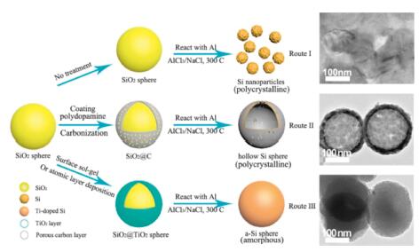
Silicon (Si) is a potential substitute for the commercial anode-material, graphite, for lithium-ion batteries (LIBs) [1-5]. It has a remarkable theoretical capacity of ~4200 mAh/g, 10 times higher than that (372 mAh/g) of graphite, by forming Li22Si5 alloy during the lithiation [6-10]. Moreover, the abundant resource of Si makes it attractive for energy storage. However, several obvious drawbacks impede its practical application in LIBs. A large volume expansion occurs during the lithiation/delithiation process, which may cause the cracking of Si and its peeling from the current collector. Thus, Si-based electrodes lose the activity during the cycling, resulting in the poor electrochemical performance. Si nanomaterials (e.g., porous Si, nanospheres, nanosheets, nanowires, hollow structures) have been found to be of improved performance while most of them are crystalline materials [11-18]. Their performance can be further enhanced by doping other elements such as boron, phosphorus and sulfur. They can be usually achieved by laser ablation, ball-milling and chemical vapor deposition (CVD) methods [19-23]. Recently, amorphous silicon (a-Si) has been found more attractive than crystalline one since Si eventually turns into the amorphous phase after the lithiation/delithiation process. a-Si is more endurable to the structural fracture because only isotropic strain/stress is involved during lithiation/delithiation [24]. Furthermore, it reacts with Li at a higher potential (0.22 V) than crystalline silicon (c-Si) (0.12 V) [25]. The cut-off potential during lithiation can be raised so that the lithium dendrites and the volume expansion can be effectively restrained. Therefore, a-Si exhibits high capacity and excellent cyclability.Via a two-stage laser pyrolysis of silane and ethylene, Sourice et al. have synthesized core-shell amorphous silicon-carbon nanoparticles [26]. The prepared anode retains a capacity of 1250 mAh/g at 715.8 mA/g after 500 cycles. Sakabe et al. have fabricated porous amorphous Si film anodes via magnetron sputtering, which delivers 2962 mAh/g and 2.19 mAh/cm2 after 100 cycles [27]. Kim et al. have synthesized amorphous Si and edge-plane activated graphite composite via CVD method, with an exceptional initial Coulombic efficiency (ICE) of 93.8% [28]. With the thermal decomposition of trisilane, McDowell et al. have synthesized hydrogenated amorphous Si spheres with a size of up to 870 nm with good fracture-endurance during the lithiation [29]. The above preparation processes involving expensive precursors usually lack of scalability. Compared with them, reduction of silicon oxide with metals (e.g., Al, Mg) is a more straightforward and scalable way to prepare Si nanostructures. For example, Mg vapor has been used to reduce biosilica templates into Si nanostructures with the shape-preservation at 650 ℃. Zhu et al. have demonstrated that Al powder can reduce the silicon oxide into Si nanoparticles at a temperature as low as 250 ℃ in the molten AlCl3, as shown as Route I in Fig. 1. Inspired by the above findings, our group has successfully synthesized the hollow Si spheres from SiO2 spheres by using the carbon layer as the diffusion layer in the molten AlCl3/NaCl, following the route II in Fig. 1 [30]. Though the temperature in the above reduction process is low enough, the Si products are still polycrystalline. The result also indicates that the additional layer on the silica precursor can strongly influence the morphology of Si product.

|
Download:
|
| Fig. 1. Schematic illustration of the synthesis of the Si nanoparticles, hollow Si spheres and a-Si spheres reduced from the silica spheres without treatment (Route I), with carbon coating (Route II) and TiO2 coating (Route III), respectively. | |
In this study, we coated the silica spheres with TiO2 nanolayer and reacted them with Al powder in the NaCl/AlCl3 mixture. The coated TiO2 layer facilitated the formation of a-Si during the reduction. The as-prepared a-Si spheres displayed a good structural stability in the lithiation/delithiation process, as observed by in-situ transmission electron microscopy (TEM). The anode with a-Si spheres delivers reversible capacities of 2763.3 mAh/g at 1 A/g and 1604 mAh/g at 4 A/g, respectively. Besides, it maintains 78.3% capacity retention after 500 cycles at 4 A/g.
The a-Si spheres were prepared as follows. Firstly, SiO2 spheres were synthesized by the modified Stöber method [31]. Specifically, 9 mL ammonia was mixed with 24.75 mL absolute ethanol and 16.25 mL deionized water. Then, 0.67 mL tetraethyl orthosilicate (TEOS) together with 45.5 mL absolute ethanol was poured into the above ammonia solution rapidly. After stirring at room temperature for 30 min, the mixed solution turned into white colloidal suspension. The SiO2 spheres were finally collected after centrifugation and drying. Then, they were coated with TiO2 layers via a surface-sol-gel (SSG) process [32]. Specifically, ~300 mg SiO2 sphere powder was immersed into 10 mL solution of ethanol/toluene with 1:1 volume ratio. Then, a certain amount of titanium n-butoxide (Ti-(OnBu)4) was diluted in the ethanol/toluene mixture to form a 100 mmol/L solution. After 10 min soaking, the SiO2 spheres with Ti-(OnBu)4 on surface were centrifuged and washed with ethanol for 5 times, followed by hydrolyzing in DI water for 1 min. After repeating the above process of immersing and hydrolysis for 10 times, the SiO2 spheres coated with TiO2 (SiO2@TiO2) were collected after centrifugation and drying in air. The SiO2@TiO2 spheres were reduced to silicon with metallic Al in molten salts as our previous research [33]. The SiO2@TiO2 powder of ~200 mg was mixed with Al, NaCl and AlCl3 with a molar ratio of about 1:1.9:3:4.5. The Al powder used here is 1000 mesh in size (~13 μm in diameter). Then, the mixture was sealed into an autoclave and placed in a tube furnace. After the annealing of 300 ℃ for 12 h, the reaction product was etched by HCl and HF, followed by washing with DI water and ethanol. The final Si spheres were obtained after centrifugation and drying in vacuum.
The samples were characterized by scanning electron microscopy (SEM, Zeiss Ultra 55), X-ray diffraction (XRD) analyses (Rigaku D/Max-RB diffractometer with Cu Kα radiation), Raman spectra (Renishaw Raman spectrometer). Compositions of a-Si were analyzed using an Agilent 700 inductively coupled plasma-optical emission spectrometer (ICP-OES). TEM and scanning TEM (STEM) were performed using a JEOL JEM-2100F TEM/STEM operated at 200 kV, equipped with a Gatan Enfina electron spectrometer. Electron energy-loss spectroscopy (EELS) mapping was carried out under 200 kV accelerating voltage with a 13 mrad convergence angle for the optimal probe condition. Energy dispersion of 0.7 eV per channel and a 21 mrad collection angle were set up for EELS, with high-angle annular dark field (HAADF) images acquired with an 89 mrad inner angle simultaneously. The Si, O and Li elemental maps were extracted from the EELS mapping by integrating across the energy windows of 99–130 (Si L2, 3 edge), 532–567 (O K edge) and 55–63 (Li K edge) eV, respectively. For in-situ TEM, the a-Si spheres were loaded onto an electrochemical-etched micro-size tungsten tip and fixed with conductive silver epoxy. Another tungsten tip with submicron size at the end was used to scratch the fresh lithium metal surface in an argon glove box and attached to a piezo-driven biasing probe built into the Nanofactory TEM scanning tunneling microscopy (TEM-STM) holder. Before taking the holder into the ambient air, the holder tip was sealed by a plastic cap and then wrapped by a Parafilm tape. Once the sealed holder was taken out from the glovebox, it was inserted into the TEM column as quickly as possible for immediate in-situ lithiation study by TEM. The Li2O on the Li metal surface serves as a solid electrolyte. A −5 V voltage bias was applied between the Li metal tip and Si tip. The in-situ videos were taken with 0.5 s/frame and the corresponding dose rate (number of electrons per square angström per second, e Å−2 s-1) ~2.8 e Å−2 s-1.
Electrochemical performances of samples were tested on 2016 coin-type cells. The working electrode was composed of Si nanoparticles or a-Si, sodium alginate, and Super P carbon black with a weight ratio of 60:20:20 spread on a piece of Cu foil. The mass loading of active materials was ~1 mg/cm2. Coin-type half-cells were assembled in an argon-filled glovebox. Lithium foils were used as the counter electrode. A 1mol/L LiPF6 solution in ethylene carbonate and diethyl carbonate (1:1 in volume) with 10 wt% fluoroethylene carbonate was used as the electrolyte. The cells were tested in the voltage range of 0.01 − 1.0 V (vs. Li/Li+) at 25 ℃. Electrochemical impedance spectroscopy (EIS) was recorded by an electrochemical workstation (AutoLab 302 N) from 1 MHz to 10 mHz.
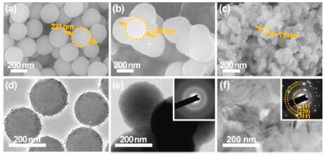
Route III in Fig. 1 illustrates the preparation process of a-Si spheres. The raw silica nanospheres were prepared through the modified Stöber method [31]. An ultrathin layer of TiO2 was then coated on the surface of the silica spheres via the surface-sol-gel (SSG) method [32, 34]. Specifically, the Ti-(OnBu)4 was firstly chemisorbed on the surface of SiO2 spheres through hydroxyl groups. Then it was converted to TiO2 through hydrolysis in water, along with the reproduction of a new uniform hydroxyl surface. After several repetitions of the process, the TiO2 layer was successfully coated on the silica spheres. Afterward, the as-prepared TiO2-coated SiO2 (SiO2@TiO2) spheres were converted to a-Si spheres after being reacted with Al powder in the molten salts of NaCl and AlCl3 together with HCl etching. For comparison, Si nanoparticles were also prepared from uncoated silica spheres via the same reduction process as shown in Route I in Fig. 1.
Fig. 2a shows the SEM image of the raw silica spheres synthesized via the modified Stöber method. The spheres with quite smooth surfaces exhibit a uniform diameter of 209.5 ± 17.5 nm. The SiO2@TiO2 spheres shown in the TEM image (Fig. 2d) possess relatively rough surfaces due to the coated TiO2 layers derived from the SSG method. It is consistent with the SEM images (Figs. S1a and b in Supporting information) of the SiO2@TiO2 spheres. Furthermore, the energy dispersive spectroscopy (EDS) analysis in Fig. S1c (Supporting information) confirms the existence of the TiO2. It is amorphous since no sharp peaks appear in the XRD pattern (Fig. S2 in Supporting information) of SiO2@TiO2 spheres, which possesses good buffering properties to protect the structure in reaction [35]. Fig. S3a (Supporting information) displays an enlarged TEM image of the SiO2@TiO2 spheres. The thickness of the TiO2 layer is estimated to be ~3 nm. The EELS mapping in Fig. S3b (Supporting information) further proves the uniform coating of TiO2 on the surface of SiO2 sphere. Figs. 2b and e and Fig. S4 (Supporting information) show the SEM and TEM images of the product reduced from SiO2@TiO2 with Al powder in the molten NaCl/AlCl3. The product contains the aggregated spheres with a little larger size (240.4 ± 27.1 nm) than the original silica nanospheres. Meanwhile, irregular nanoparticles are also observed as shown in Fig. S5 (Supporting information). On contrary, the SEM (Fig. 2c) and TEM (Fig. 2f) images of the Si nanoparticles reveal that the silica spheres were only reduced into irregular nanoparticles. The bulk density of a-Si spheres can be theoretically calculated to be 0.54 g/cm3 based on the volume change after reaction. (The detailed method of calculation is in the Supporting information.) The density is much lower than the reported values (2.19–2.29 g/cm3) of the amorphous Si, indicating that lots of defects such as pores and vacancies may exist [36]. The EELS mapping (Fig. S6c in Supporting information) indicates that the product is mainly composed of Si with a trace of O enrichment at the surface, which results from the exposure to the air [37]. The signal from Ti element is weak and diffusive, which may be due to the inward diffusion of Ti atoms from the surface of sphere in reaction. The analyses based on inductively coupled plasma-optical emission spectrometer (ICP-OES) in Table S1 (Supporting information) indicate its weight ratio was 3 × 10⁻³ in a-Si product. Thus a-Si is doped with a trace amount of Ti element, which was simultaneously reduced from TiO2 layer by Al in the reduction. Its selected area electron diffraction (SAED, the inset in Fig. 2e) without clear diffraction spots confirms the amorphous phase while the SAED pattern of Si nanoparticles (the inset in Fig. 2f) presents high crystallinity. More SAED patterns (Figs. S7c–e in Supporting information) of other spheres formed from TiO2-coated silica and their high-resolution TEM (HRTEM) image (Fig. S7b in Supporting information) further confirm their amorphous nature. However, XRD pattern of the a-Si product (Fig. S8 in Supporting information) reveals the presence of the crystalline phase. The extent of amorphization is calculated to be 66.7% (The detailed method of calculation is in the Supporting information). The TEM image and SAED pattern as shown in Fig. S5 (Supporting information) reveal that the product also contains the irregular silicon particles with good crystallinity. The particles are of the similar morphology and crystallinity as the product from the uncoated silica sphere. The Raman spectra of Si nanoparticles and a-Si product exhibit the similar features as shown in Fig. S9 (Supporting information). The peaks around 510 cm-1 indicate the formation of Si-Si bond. However, the peak of a-Si is weaker than that of Si nanoparticles, indicating the poor crystallinity of a-Si [38, 39]. And there is ~5 cm-1 shift between the two products due to the presence of both amorphous phase of Si and smaller Si crystals in a-Si product [38, 40, 41]. Furthermore, a broad shoulder emerging around 470 cm-1 is also related to the formation of a-Si (TO vibration of a-Si) [27]. The partial crystallinity of a-Si product is from the irregular nanoparticles, which are the reaction product of the silica spheres with unperfect TiO2 coating layer. The amorphous phase accounts for 50% overall weight, which is consistent with the estimation from XRD patterns (The detailed method of calculation is in the Supporting information).

|
Download:
|
| Fig. 2. Microstructure of the raw silica and the as-prepared Si products. SEM images of (a) SiO2 spheres, (b) a-Si spheres and (c) Si nanoparticles. TEM images of (d) SiO2@TiO2 spheres, (e) a-Si spheres and (f) Si nanoparticles. The insets in (e) and (f) are the SAED patterns of a-Si spheres and Si nanoparticles, respectively. | |
When heated to 300 ℃, the mixture of AlCl3-NaCl was converted to liquid phase as the molar ratio of AlCl3 and NaCl was 3:2 [30, 42, 43]. Al was solvated in the liquid molten salts and composed Al-AlCl complex with molten AlCl3. Furthermore, the activated AlCl* was formed from the Al-AlCl complex [44]. For the raw silica precursor, the activated AlCl* could directly contact the surface of the SiO2 sphere followed by the capture of oxygen atoms. Afterward, the Si-Si bond was formed together with the byproduct AlOCl. Meanwhile, the AlCl4− was produced from the NaCl and AlCl3 mixture and ultimately composed NaAlCl4 [45]. The overall reaction can be concluded as the following equation:

|
(1) |
In the case of the silica nanospheres as the reactant, after losing oxygen atoms, Si atoms detached from the unreacted silica part and diffused randomly in the molten salts. This induced the breakdown of the spherical structure, as shown in Fig. S10a (Supporting information). Eventually, Si atoms were assembled into the crystalline nano-clusters, which ultimately formed Si nanoparticles via Ostwald ripening process to optimize the surface energy [30, 46]. However, in the case of that SiO2@TiO2 spheres were reacted with Al in the molten salts, amorphous TiO2 layers might be reduced to Ti, doping into the reduced Si [47]. Ti atoms gradually diffused inward from the surface of sphere in the reaction and eventually formed a relatively homogeneous distribution in Si. The introduction of Ti atoms might effectively hinder the interdiffusion of Si atoms so that it was hard for Si atoms to optimize their position for crystallization. The above mechanism was illustrated in Fig. S10b (Supporting information). Meanwhile, the low reduction temperature at 300 ℃ and the molten salt as the heat scavenger also facilitated the formation of the amorphous phase. In the case of the hollow Si spheres, however, the carbon layer could not effectively hinder the diffusion of Si atoms due to its porosity. Instead, it could provide sites for the nucleation of Si. Thus, the hollow Si spheres present higher crystallinity than a-Si spheres.
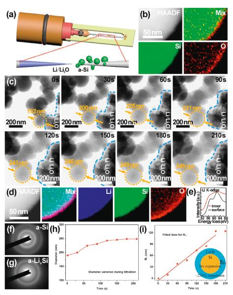
To further explore the lithiation process of a-Si spheres, the in-situ TEM experiment was carried out. The in-situ TEM followed a similar design as reported by Wang et al. and Li et al., schematically illustrated in Fig. 3a [48-50]. The a-Si spheres were loaded onto an electrochemically etched micro-size tungsten tip and fixed with conductive silver epoxy. Another tungsten tip with submicron size at the top was used to scratch fresh lithium metal surface. The Li2O on the Li metal surface was served as a solid electrolyte. A −5 V voltage bias was applied between Li metal tip and a-Si tip. Since the dose rate of the electron beams used here was relatively low (~2.8 e Å−2 s-1) and the in-situ reaction time was short, the Li metal might hardly become quasi-melted, caused by electron beams. Thus, there was no obvious effect on the lithiation of a-Si spheres. Fig. 3b shows the EELS maps of a-Si sphere before lithiation, which is mainly composed of Si elements. After lithiation, lithium element appeared, and the spheres expanded as shown in in-situ TEM image series (Fig. 3c). The lithiation process completed at 180 s as the volume change almost stopped. The corresponding average volume expansion is displayed in Fig. S11 (Supporting information), which indicates the 233% average volume expansion after the complete lithiation. However, it is reported that c-Si spheres cracked during lithiation when the diameter was larger than 150 nm, while the lithiated a-Si spheres maintained their intrinsic structure even up to 870 nm in diameter [29, 51]. Compared with c-Si, the a-Si may result in less tensile stress due to the isotropic expansion [52]. Besides, the concentration of Li in the LixSi phase of a-Si, which forms as the Si-Si bonds in Si matrix crack in lithiation, is lower than that of c-Si. Similar to the SAED pattern of a-Si in Fig. 3f, that of the lithiated product LixSi in Fig. 3g indicates it is still amorphous, consistent with the previous work [29]. Thus, less expansion and lower stress occurs in the a-Si than c-Si. Additionally, the native oxide layer of a-Si spheres can buffer the volume expansion during lithiation as well. As seen in the EELS maps in Fig. 3d, O element gathered at the surface of sphere together with Li, indicating the reaction on the surface related to the formation of Li2O during lithiation, which could further enhance the transport of Li ions [53]. Indeed, the Li K-edge spectrum at the surface of a-Si sphere given in Fig. 3e is consistent with the Li2O phase [54]. It was formed via the reaction between Li and SiOx, which was beneficial for accommodating the volume expansion [55, 56]. On the basis of the time series of lithiation in Fig. 3c, the kinetic process can be further investigated. The darker Si-rich cores and the lighter Li-rich shells can be observed during lithiation. The dark cores remain spherical, indicating the fast diffusion of Li through all surfaces homogeneously [57]. With lithiation going, the dark Si-rich cores gradually shrunk while the light Li-rich shells expanded. To further explore the change of the lithiation depth, the overall diameter variation of a picked sphere is shown in Fig. 3h. The volume expanded rapidly in the early stage of the lithiation mainly due to the relatively large contact area between the a-Si spheres and the Li metal. As the lithiation went deeper into the cores, the volume expanded more slowly, and the diameter reached the maximum value at 180 s as the lithiation completed. Since the lithiation depth, the radial distance from the surface to the dark Si-rich core boundary, could not be obtained clearly in Fig. 3c, it was calculated on the basis of the volume change during lithiation. It was assumed that Li+ diffused inward along the radius of sphere and that the volume change of the lithiated parts was 233% as shown in the bottom right inset of Fig. 3i. Thus, the lithiation depth RLi could be obtained as shown in Fig. 3i. The RLi increases linearly with time approximately, indicating that the kinetics of lithiation is determined by the short-range interfacial reaction [29]. The lithiation is limited by the reaction rate at the interface. For this interface-controlled reaction, the lithiation slowed as it progressed into the interior of the structure due to the changing mechanical stress at the interface [57, 58]. The light Li-rich shell expanded homogeneously, leading to less tensile stress and keeping the integrity of spherical structure. Li+ diffusivity of a-Si anode could be roughly calculated based on the above lithiation kinetics as shown in Table S2 (Supporting information). It was estimated to be in the order of 10-14 cm2/s according to the diffusional model of spherical solid particles.

|
Download:
|
| Fig. 3. Volume expansion of a-Si spheres during in-situ lithiation. (a) Schematic illustration of the in-situ lithiation holder setting. (b) EELS elemental maps and the simultaneous HAADF-STEM image of the pristine a-Si sphere. (c) Time series of the lithiation of a-Si spheres. (d) EELS elemental maps and the simultaneous HAADF-STEM image of the same a-Si sphere after lithiation. (e) Li K-edge EELS spectra from the surface and inner part of the selected a-Si sphere after lithiation. (f, g) SAED patterns of the selected a-Si sphere (f) before and (g) after in-situ lithiation. (h) The diameter vs. time of the picked a-Si sphere during lithiation. (i) Relationship between the lithiation depth and time. The bottom right inset is the schematic illustration of the calculated process of lithiation depth. | |
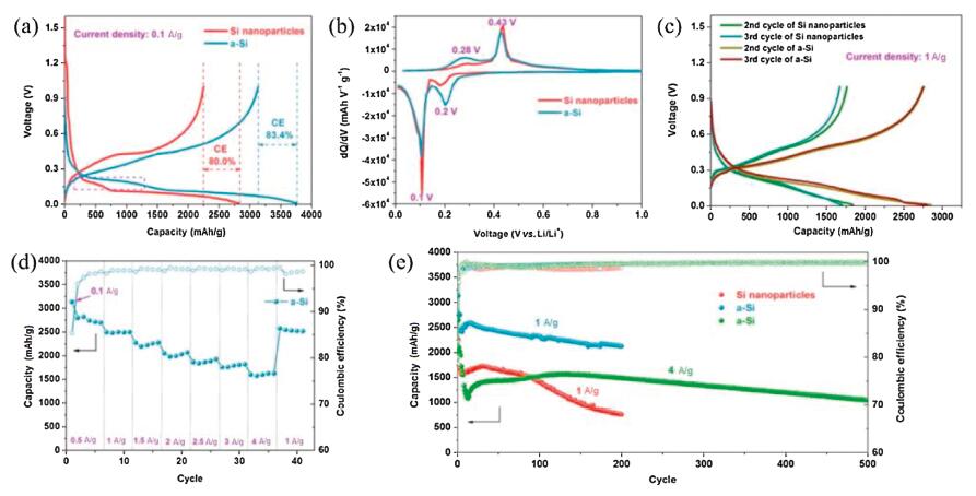
The electrochemical performance of the anodes with crystalline Si nanoparticles or a-Si product (partially with crystalline Si nanoparticles) was examined in the half cells with lithium metal as the counter electrodes. The test voltage ranges from 0.01−1 V. The initial galvanostatic voltage profiles of Si nanoparticles and a-Si at 0.1 A/g are given in Fig. 4a. The Si-nanoparticle electrode delivers an initial discharge capacity of 2815.7 mAh/g and the a-Si electrode achieves 3759.3 mAh/g. The ICE of Si-nanoparticle and a-Si electrodes is calculated to be 80% and 83.4%, respectively. The higher ICE of a-Si electrode is due to the larger particle size of a-Si spheres, which leads to reduced side reaction during the formation of solid electrolyte interphase (SEI). The irreversible capacity of the first cycle can be further reduced by the introduction of an artificial SEI layer (e.g., carbon, alumina, TiO2, polymers) or prelithiation of the electrode [30, 59-63]. Fig. 4b displays the plots of the differential capacity versus voltage of the Si-nanoparticle and a-Si electrodes. In the both two electrodes, two peaks at ~0.1 V and ~0.2 V can be observed, which are related to the lithiation of crystalline Si and amorphous Si, respectively [40, 64-66]. The intensity of the peak of a-Si at 0.2 V is much higher than that of Si nanoparticles, consistent with the longer voltage platform in the rectangular area in Fig. 4a. Fig. 4c provides the galvanostatic voltage profiles of the second and third cycles at a current density of 1 A/g of Si nanoparticles and a-Si electrodes, respectively. It can be clearly seen that there's no voltage platform at 0.1 V, indicating the disappearance of crystalline silicon after the first cycle. Moreover, a-Si electrode presents no obvious capacity decay due to its stable structure. The cycling performance of Si nanoparticles and a-Si at the current density of 1 A/g is shown in Fig. 4e. The reversible capacities of 1762.6 and 2763.3 mAh/g at 1 A/g can be achieved for Si-nanoparticle and a-Si electrodes, respectively. After 200 cycles, the electrode of Si nanoparticles exhibits only 43.1% capacity retention, while the a-Si electrode holds 76.8% of the initial capacity. Besides, the CE of a-Si electrode achieves more stable values (> 99%) after a few cycles than that of Si nanoparticles. Furthermore, the a-Si electrode delivers a reversible capacity of 1339.6 mAh/g at 4 A/g and maintains 78.3% capacity retention even after 500 cycles. It is due to the high resistance of a-Si to structure fracture, resulting in more stable SEI layers than c-Si [29, 41, 67]. The a-Si spheres were kept separated and stable in spherical structure after cycling as indicated in Fig. S12a (Supporting information) while the aggregation of Si nanoparticles would inevitably occur after the cycling as shown in Fig. S12b (Supporting information). Additionally, the low density of a-Si also accommodates more volume expansion. Thus, a-Si exhibits good cycling performance. Fig. 4d reveals the rate performance of the a-Si electrode. The reversible capacities of 2800, 2494, 2274, 2050, 1865, 1755 and 1604 mAh/g at the current densities of 0.5, 1, 1.5, 2, 2.5, 3 and 4 A/g are achieved, respectively. The good rate performance of the a-Si electrode is attributed to the improved charge transport resulted from the Ti doping. In all, the a-Si electrode presents more excellent electrochemical performance than Si nanoparticles.

|
Download:
|
| Fig. 4. Electrochemical performance of Si nanoparticles and a-Si electrodes. (a) Galvanostatic discharge/charge voltage profiles of the first cycle at a current density of 0.1 A/g of Si nanoparticles and a-Si electrodes. (b) Plots of the differential capacity versus voltage. (c) Galvanostatic discharge/charge voltage profiles of the second and third cycles at a current density of 1 A/g of Si nanoparticles and a-Si electrodes. (d) Rate capability of a-Si electrode. (e) Long-term cycling stability of Si nanoparticles and a-Si electrodes. | |
The electrochemical impedance spectrum (EIS) was performed to investigate the charge transport kinetics in the electrochemical test process. The equivalent circuits for the Si-nanoparticle and a-Si anodes before and after cycling are shown in Figs. S13a and c (Supporting information), respectively. In these circuits, Rs is the electrolyte resistance, Rct is the charge transfer resistance of the Si products and Rf is the charge transfer resistance of SEI layer [68]. In the Nyquist plots of the Si-nanoparticle and a-Si anodes before cycling in Fig. S13a, typical semicircles in the high-frequency area can be observed, which is related to Rct. As the fitting results shown in Table S3a (Supporting information), the Rct value of the a-Si anode is higher than that of the Si-nanoparticle anode. Fig. S13b (Supporting information) exhibits the linear fitting between Z' and ω−1/2, where the slope represents the Warburg factor σ. The Li+ diffusion coefficient D can be calculated on the basis of σ (The detailed method of calculation is in the Supporting information). The D value (2.14 × 10⁻¹⁷ cm2/s) of the a-Si anode is lower than that (5.12 × 10⁻¹⁷ cm2/s) of the Si-nanoparticle anode as shown in Table S3a (Supporting information). It's due to the much smaller initial size of the Si nanoparticles leading to the shorter diffusion paths of Li+. However, the D value (2.37 × 10⁻¹⁴ cm2/s) of the a-Si anode becomes larger than that (4.81 × 10⁻¹⁵ cm2/s) of the Si-nanoparticle anode after cycling in Table S3b (Supporting information), together with a lower Rf in a-Si. Because the a-Si spheres kept the original structure after cycling, resulting in the stable SEI layer at the interface of the electrode and electrolyte. Both the D values of the Si nanoparticles and the a-Si anodes after cycling are much larger than those of them before cycling, respectively. It is mainly ascribed to the activation of active materials and the enhanced electrolyte wetting during cycling [69, 70]. The D value of a-Si spheres was in the same order of magnitude as the results of in-situ TEM. Nevertheless, the Si nanoparticles smashed and recombined into bulk during the repeated expanding and shrinking process, leading to the relatively long Li+ diffusion paths and the instability of the SEI layer [71].
In summary, the amorphous silicon spheres were synthesized via reducing the TiO2-coated silica spheres with Al powders in the molten salts. The TiO2 layer plays an important role in the structural maintenance and the formation of the amorphous phase of Si spheres. The as-prepared a-Si anode achieves an excellent electrochemical performance, delivering a reversible capacity of 1604 mAh/g at 4 A/g and a capacity retention of 78.3% after 500 cycles. This work provides a facile and low-cost method to fabricate amorphous Si, which can be widely used to produce other amorphous silicon-based materials with various morphologies.
Declaration of competing interestThe authors declare that they have no known competing financial interests or personal relationships that could have appeared to influence the work reported in this paper.
AcknowledgmentsThis work was supported by National Key Research and Development Program of China (No. 2017YFA0204600), National Natural Science Foundation of China programs (Nos. U1703128, U1503292) and the Hong Kong Polytechnic University (No. 1-ZVRP).
Appendix A.Supplementary dataSupplementary material related to this article can be found, in the online version, at doi:https://doi.org/10.1016/j.cclet.2020.11.041.
| [1] |
M.A. Rahman, G. Song, A.I. Bhatt, Y.C. Wong, C. Wen, Adv. Funct. Mater. 26 (2016) 647-678. DOI:10.1002/adfm.201502959 |
| [2] |
H. Zhao, W. Yuan, G. Liu, Nano Today 10 (2015) 193-212. DOI:10.1016/j.nantod.2015.02.009 |
| [3] |
X. Zuo, J. Zhu, P.Müller-Buschbaum, Y.J. Cheng, Nano Energy 31 (2017) 113-143. DOI:10.1016/j.nanoen.2016.11.013 |
| [4] |
W. Luo, X. Chen, Y. Xia, et al., Adv. Energy Mater. 7 (2017) 1701083. DOI:10.1002/aenm.201701083 |
| [5] |
M. Ashuri, Q. He, L. Shaw, Nanoscale 8 (2015) 74-103. |
| [6] |
K. Feng, W. Ahn, G. Lui, et al., Nano Energy 19 (2016) 187-197. DOI:10.1016/j.nanoen.2015.10.025 |
| [7] |
J. Liu, Q. Zhang, T. Zhang, et al., Adv. Funct. Mater. 25 (2015) 3599-3605. DOI:10.1002/adfm.201500589 |
| [8] |
Z. Luo, Q. Xiao, G. Lei, Z. Li, C. Tang, Carbon 98 (2016) 373-380. DOI:10.1016/j.carbon.2015.11.031 |
| [9] |
J.-L. Shi, D.-D. Xiao, X.-D. Zhang, et al., Nano Res. 10 (2017) 4201-4209. DOI:10.1007/s12274-017-1489-3 |
| [10] |
R. Yi, M. Gordin, D. Wang, Nanoscale 8 (2016) 1834-1848. DOI:10.1039/C5NR07625K |
| [11] |
W. An, B. Gao, S. Mei, et al., Nat. Commun. 10 (2019) 1447-1457. DOI:10.1038/s41467-019-09510-5 |
| [12] |
M. Sohn, D.G. Lee, H.I. Park, et al., Adv. Funct. Mater. 28 (2018) 1800855. DOI:10.1002/adfm.201800855 |
| [13] |
J. Liang, X. Li, Q. Cheng, et al., Nanoscale 7 (2015) 3440-3444. DOI:10.1039/C4NR07642G |
| [14] |
L. Luo, H. Yang, P. Yan, et al., ACS Nano 9 (2015) 5559-5566. DOI:10.1021/acsnano.5b01681 |
| [15] |
X. Wang, G. Li, M.H. Seo, et al., ACS Appl. Mater. Interfaces 9 (2017) 9551-9558. DOI:10.1021/acsami.6b12080 |
| [16] |
J. Ryu, T. Chen, T. Bok, et al., Nat. Commun. 9 (2018) 2924-2931. DOI:10.1038/s41467-018-05398-9 |
| [17] |
S. Chen, Z. Chen, X. Xu, et al., Small 14 (2018) 1703361. DOI:10.1002/smll.201703361 |
| [18] |
Q. Zhang, H. Chen, L. Luo, et al., Energy Environ. Sci. 11 (2018) 669-681. DOI:10.1039/C8EE00239H |
| [19] |
G. Lv, B. Zhu, X. Li, et al., ACS Appl. Mater. Interfaces 9 (2017) 44452-44457. DOI:10.1021/acsami.7b12898 |
| [20] |
S.K. Bux, R.G. Blair, P.K. Gogna, et al., Adv. Funct. Mater. 19 (2009) 2445-2452. DOI:10.1002/adfm.200900250 |
| [21] |
N. Fukata, Adv. Mater. 21 (2009) 2829-2832. DOI:10.1002/adma.200900376 |
| [22] |
M. Ali, F. Zhou, K. Chen, et al., Nat. Commun. 7 (2016) 11335. DOI:10.1038/ncomms11335 |
| [23] |
G. Zhu, R. Guo, W. Luo, et al., Nat. Sci. Rev. (2020) nwaa152. DOI:10.1093/nsr/nwaa152 |
| [24] |
M. McDowell, S.W. Lee, W.D. Nix, Y. Cui, Adv. Mater. 25 (2013) 4966-4985. DOI:10.1002/adma.201301795 |
| [25] |
L.-F. Cui, R. Ruffo, C. Chan, H. Peng, Y. Cui, Nano Lett. 9 (2009) 491-495. DOI:10.1021/nl8036323 |
| [26] |
J. Sourice, A. Bordes, A. Boulineau, et al., J. Power Sources 328 (2016) 527-535. DOI:10.1016/j.jpowsour.2016.08.057 |
| [27] |
J. Sakabe, N. Ohta, T. Ohnishi, K. Mitsuishi, K. Takada, Commun. Chem. 1 (2018) 24. DOI:10.1038/s42004-018-0026-y |
| [28] |
N. Kim, S. Chae, J. Ma, M. Ko, Nat. Commun. 8 (2017) 812. DOI:10.1038/s41467-017-00973-y |
| [29] |
M.T. McDowell, S.W. Lee, J.T. Harris, et al., Nano Lett. 13 (2013) 758-764. DOI:10.1021/nl3044508 |
| [30] |
P. Gao, X. Huang, Y. Zhao, et al., ACS Nano 12 (2018) 11481-11490. DOI:10.1021/acsnano.8b06528 |
| [31] |
W. Stöber, A. Fink, E. Bohn, J. Colloid Interface Sci. 26 (1968) 62-69. DOI:10.1016/0021-9797(68)90272-5 |
| [32] |
I. Ichinose, H. Senzu, T. Kunitake, Chem. Mater. 9 (1997) 1296-1298. DOI:10.1021/cm970008g |
| [33] |
X. Huang, D. Cen, R. Wei, H. Fan, Z. Bao, ACS Appl. Mater. Interfaces 11 (2019) 26854-26862. DOI:10.1021/acsami.9b06976 |
| [34] |
M. Li, X. Li, W. Li, et al., Electrochem. Commun. 57 (2015) 43-47. DOI:10.1016/j.elecom.2015.05.005 |
| [35] |
J. Yang, Y. Wang, W. Li, et al., Adv. Mater. 29 (2017) 1700523. DOI:10.1002/adma.201700523 |
| [36] |
Z. Remeš, M. Vaněček, P. Torres, et al., J. Non·Cryst. Solids 227-230 (1998) 876-879. DOI:10.1016/S0022-3093(98)00207-5 |
| [37] |
Q. Chen, R. Zhu, Q. He, et al., Chem. Commun. 55 (2019) 2644-2647. DOI:10.1039/C8CC10036E |
| [38] |
J. Lang, B. Ding, S. Zhang, et al., Adv. Mater. 29 (2017) 1701777. DOI:10.1002/adma.201701777 |
| [39] |
D. Yu, Z.G. Bai, Y. Ding, et al., Appl. Phys. Lett. 72 (1998) 3458. DOI:10.1063/1.121665 |
| [40] |
P. Gao, H. Tang, A. Xing, Z. Bao, Electrochim. Acta 228 (2017) 545-552. DOI:10.1016/j.electacta.2017.01.119 |
| [41] |
L. Lin, X. Xu, C. Chu, M.K. Majeed, J. Yang, Angew. Chem. Int. Ed. 55 (2016) 14063-14066. DOI:10.1002/anie.201608146 |
| [42] |
E.M. Levin, J.F. Kinney, R.D. Wells, J.T. Benedict, J. Res, Natl. Bur. Stand. 78A (1974) 505-507. DOI:10.6028/jres.078A.033 |
| [43] |
C.W. Bale, P. Chartrand, S.A. Degterov, et al., Calphad 26 (2002) 189-228. DOI:10.1016/S0364-5916(02)00035-4 |
| [44] |
G. Song, J. Ryu, J.C. Kim, et al., Commun. Chem. 1 (2018) 42-51. DOI:10.1038/s42004-018-0041-z |
| [45] |
A. Bjørgum, Å.Sterten, J. Thonstad, R. Tunold, Electrochim. Acta 26 (1981) 491-496. DOI:10.1016/0013-4686(81)87028-4 |
| [46] |
X. Liu, C. Giordano, M. Antonietti, J. Mater. Chem. 22 (2012) 5454. DOI:10.1039/c2jm15453f |
| [47] |
S. Alamolhoda, S. Heshmati-Manesh, A. Ataie, A. Badiei, Adv. Mater. Res. 264-265 (2011) 626-630. DOI:10.4028/www.scientific.net/AMR.264-265.626 |
| [48] |
M. Gu, A. Kushima, Y. Shao, et al., Nano Lett. 13 (2013) 5203-5211. DOI:10.1021/nl402633n |
| [49] |
Y. Li, Q. Zhang, Y. Yuan, et al., Adv. Energy Mater. 10 (2020) 2000717. DOI:10.1002/aenm.202000717 |
| [50] |
Z. Zheng, H.H. Wu, H. Chen, et al., Nanoscale 10 (2018) 22203-22214. DOI:10.1039/C8NR07207H |
| [51] |
X.H. Liu, L. Zhong, S. Huang, et al., ACS Nano 6 (2012) 1522-1531. DOI:10.1021/nn204476h |
| [52] |
Z. Zheng, H.-H. Wu, H. Liu, et al., ACS Nano 14 (2020) 9545-9561. DOI:10.1021/acsnano.9b08575 |
| [53] |
G. Zhu, F. Zhang, X. Li, et al., Angew. Chem. Int. Ed. 58 (2019) 6669-6673. DOI:10.1002/anie.201902083 |
| [54] |
F. Wang, J. Graetz, M.S. Moreno, et al., ACS Nano 5 (2011) 1190-1197. DOI:10.1021/nn1028168 |
| [55] |
R. Fu, K. Zhang, R.P. Zaccaria, et al., Nano Energy 39 (2017) 546-553. DOI:10.1016/j.nanoen.2017.07.040 |
| [56] |
S.C. Jung, H.J. Kim, J.H. Kim, Y.K. Han, J. Phys, Chem. C 120 (2016) 886-892. |
| [57] |
M.T. McDowell, I. Ryu, S.W. Lee, et al., Adv. Mater. 24 (2012) 6034-6041. DOI:10.1002/adma.201202744 |
| [58] |
K. Zhao, M. Pharr, Q. Wan, et al., J. Electrochem. Soc. 159 (2012) A238-A243. DOI:10.1149/2.020203jes |
| [59] |
R. Gao, J. Tang, X. Yu, et al., Nano Energy 70 (2020) 104444. DOI:10.1016/j.nanoen.2019.104444 |
| [60] |
Y. Jin, S. Li, A. Kushima, et al., Energy Environ. Sci. 10 (2017) 580-592. DOI:10.1039/C6EE02685K |
| [61] |
J. Zhang, S. Fan, H. Wang, et al., ACS Appl. Mater. Interfaces 11 (2019) 13251-13256. DOI:10.1021/acsami.9b00939 |
| [62] |
Y. He, X. Yu, Y. Wang, H. Li, X. Huang, Adv. Mater. 23 (2011) 4938-4941. DOI:10.1002/adma.201102568 |
| [63] |
X. Zhang, D. Wang, X. Qiu, et al., Nat. Commun. 11 (2020) 3826. DOI:10.1038/s41467-020-17686-4 |
| [64] |
M.N. Obrovac, L.J. Krause, J. Electrochem. Soc. 154 (2007) A103-A108. DOI:10.1149/1.2402112 |
| [65] |
J.P. Maranchi, A.F. Hepp, P.N. Kumta, Electrochem. Solid-State Lett. 6 (2003) A198-A201. DOI:10.1149/1.1596918 |
| [66] |
M.K. Datta, P.N. Kumta, J. Power Sources 194 (2009) 1043-1052. DOI:10.1016/j.jpowsour.2009.06.033 |
| [67] |
L. Zhao, D.J. Dvorak, M.N. Obrovac, J. Power Sources 332 (2016) 290-298. DOI:10.1016/j.jpowsour.2016.09.124 |
| [68] |
X. Feng, J. Yang, Y. Bie, et al., Nanoscale 6 (2014) 12532-12539. DOI:10.1039/C4NR03948C |
| [69] |
Q. Chen, R. Zhu, S. Liu, et al., J. Mater. Chem. A 6 (2018) 6356-6362. DOI:10.1039/C8TA00587G |
| [70] |
H.S. Choi, S.J. Kim, H.W. Choi, et al., Curr. Appl. Phys. 17 (2017) 1087-1093. DOI:10.1016/j.cap.2017.04.020 |
| [71] |
A. Khawam, D.R. Flanagan, J. Phys. Chem. B 110 (2006) 17315-17328. DOI:10.1021/jp062746a |