 2021, Vol. 32


b School of Physics, State Key Laboratory of Crystal Materials, Shandong University, Ji'nan 250100, China;
c ARC Centre of Excellence in Exciton Science, School of Chemistry, The University of Melbourne, Parkville, Victoria 3010, Australia
In recent years, hybrid perovskites have attracted great attention in the fields of solar cells, light emitting diodes (LEDs) and photodetectors owing to their superior properties such as excellent broadband absorption, tunable electronic bandgap and high charge carrier mobility [1-8]. Despite their high device performance, light-induced halide segregation has often been observed in the hybrid perovskites which has impeded their development [9, 10]. The replacement of organic cations by metal cations such as Cs+ or Rb+, is one approach to solve the thermal instability problem due to the high energy barrier to migration of these ions [6, 11-13]. Various solution methods have been applied for the growth of inorganic perovskite crystals with tunable shape and size [14-16]. Excellent device performance has been achieved by solution-based processes. However, the production of large-scale perovskite devices for commercial applications is still challenging with solution methods owing to insufficient film thickness and undesirable phase transition problems [17-19].
A variety of deposition methods have been developed to improve film quality including optimizing the crystallization rate and surface coverage. The chemical vapor deposition (CVD) method that is generally utilized to grow high-quality electronic film materials, may offer an alternative pathway to fabricate all-inorganic perovskite crystals [20-22]. The surface flatness uniformity, crystalline quality and thickness of perovskite films can be controlled by variation of the deposition parameters such as component gradient, deposition time and temperature [19]. Additionally, films produced by CVD show better adhesion to the substrate compared to other methods. Tong et al. [23] utilized a well-controlled low temperature CVD process to fabricate an organic-inorganic hybrid perovskite photodetector with high-speed response. Large area modules have also been achieved by the CVD technology with potential industrial applications [17]. Perovskite LEDs were prepared by the CVD process with low surface roughness [19]. The optical and electrical properties of the perovskite film can be manipulated during the CVD process [24]. Unlike the precursors CH3NH3Br and PbBr2, which form one single perovskite phase CH3NH3PbBr3, the products of purely inorganic precursors CsBr and PbBr2 are complex, such as Cs4PbBr6, CsPb2Br5 and CsPbBr3. These products have their individual applications owing to their special optical and electrical properties. It is essential to control the perovskite film phase and quality, however, this is difficult to achieve due to the large melting point difference between the precursors. Therefore, the deposition temperature is a critical factor for the perovskite film growth.
In this work, the components, morphology and crystalline properties of perovskite films were controlled through changing the heating temperature (500-800 ℃) during the CVD process (details can be found in Supporting information). The photo-excited dynamics of perovskite films was visualized by the combination of spatially and temporally resolved fluorescence measurements. Finally, photodetectors based on perovskite films deposited by the CVD method were fabricated to examine their photo-response properties.
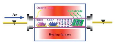
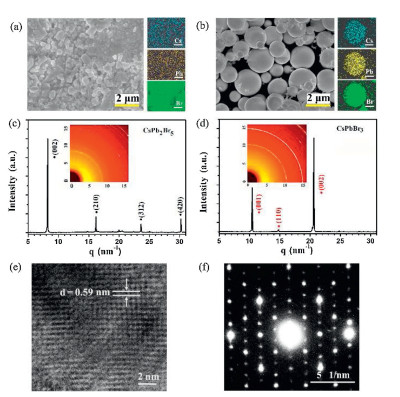
The deposition system and preparation process are schematically illustrated in Scheme 1. Fig. 1a shows the morphology of perovskite films deposited at 500 ℃ with the mean cluster size about 400 nm, which is the smallest among the five samples. The energy dispersive spectroscopy (EDS) mapping images show that the Cs, Pb and Br elements are uniformly distributed, and the ratio between the three elements is 11:23:57 (Fig. S1a in Supporting information). This ratio is very close to the stoichiometry of CsPb2Br5. As the preparation temperature increased from 600 ℃ to 750 ℃, the size of the clusters increases gradually. This was accompanied by a change in the shape of the clusters from small particles to larger spherical structures (Figs. 1a and b, Fig. S2 in Supporting information). EDS mapping of a single perovskite round cluster shows that Cs, Pb, Br elements are distributed uniformly without aggregation. The ratio between Cs, Pb, Br is 16:17:48 (Fig. S1b in Supporting information), which is very close to the stoichiometry of CsPbBr3. However, when the preparation temperature reaches 800 ℃, the morphology of the perovskite film becomes a sheet-like structure (Fig. S2c). This may be due to the high temperature inducing perovskite film degradation. These results illustrate that the deposition temperature significantly affects the morphology and composition of the perovskite film. Fig. 1c shows the XRD pattern of the perovskite film deposited at 500 ℃ with four obvious diffraction peaks of (002) at 8.2 nm-1, (210) at 16.3 nm-1, (312) at 23.8 nm-1, and (420) at 30.2 nm-1. The diffraction peaks are strong and sharp, indicating that the deposited perovskite film is quite pure CsPb2Br5 (PDF No. 25-0211) with little CsPbBr3 phase. This may be attributed to the low melting pointing of PbBr2, leading to a high content of Pb and Br. The content of CsPbBr3 increases with the deposition temperature increment, as seen from the crystalline intensity contrast between CsPb2Br5 and CsPbBr3 in Fig. S3 (Supporting information). When the deposition temperature reaches 750 ℃, three crystalline peaks (001), (110) and (002) corresponding to CsPbBr3 (PDF No. 18-0364) are apparent without CsPb2Br5 diffraction peaks, as shown in Fig. 1d. Two-dimensional diffraction image in the inset which does not reveal any diffraction signal of CsPb2Br5; even the strongest diffraction (002) located at 8.2 nm-1 is absent. This further verifies the component of the perovskite film deposited at 750 ℃ is pure CsPbBr3. The phase of all inorganic perovskite is greatly affected by the ratio between the two percursors [9]. At low deposition temperature, the proportion of PbBr2 is higher than CsBr during the reaction process owing to the lower melting point of PbBr2, leading to the formation of CsPb2Br5. With the increase of deposition temperature, especially at 750 ℃ the melting rate of CsBr increases obviously. This makes the similar ratio between PbBr2 and CsBr during the reaction process, resulting in the main component of the film is CsPbBr3. The two-dimensional diffraction images of perovskite films deposited at other temperatures are shown in Fig. S4 (Supporting information). The perovskite film deposited at 800 ℃ was degraded, as apparent in Fig. S3c. High-resolution transmission electron microscopy image (Fig. 1e) illustrates that CsPbBr3 film is a well-defined crystalline structure with a cubic lattice parameter of 0.59 nm along the (001) direction, which is consistent with the XRD data. Selected area electron diffraction (Fig. 1f) shows the bright diffraction spots, which further confirms the single crystalline property of CsPbBr3 film.

|
Download:
|
| Scheme 1. Schematic diagram of the chemical vapor deposition arrangement for the preparation of perovskite films. | |

|
Download:
|
| Fig. 1. (a, b) SEM images and EDS mapping images of perovskite films deposited at 500 ℃ and 750 ℃, respectively. (c, d) XRD spectra and two-dimensional XRD images of perovskite films deposited at 500 ℃ and 750 ℃, respectively. (e, f) High-resolution transmission electron microscopy and selected area electron diffraction of perovskite film deposited at 750 ℃. | |
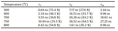
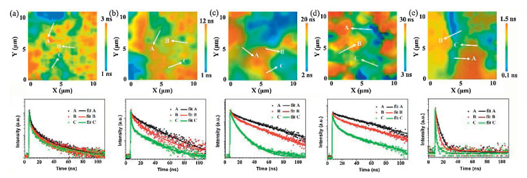
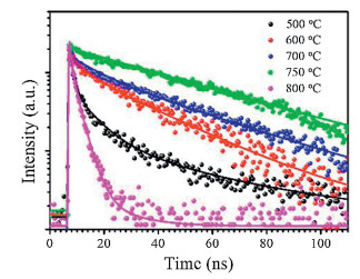
The photoluminescence (PL) maxima of the perovskite films are located in the 530-540 nm region (Fig. S5 in Supporting information). The fluorescence intensity of the perovskite film deposited at 750 ℃ is the strongest among the five samples, as shown in Fig. S6 (Supporting information). A clear red shift of the PL peak is observed as the deposition temperature increased from 500 ℃ to 750 ℃. This may be related to reabsorption effects, lattice strain and assorted changes at the grain boundaries. Sun et al. [13] emphasized that large grain size domains in perovskite films show red-shifted PL peaks compared to the small polycrystalline ones. The PL peak is blue shifted in the film deposited at 800 ℃ owing to the degradation of perovskite. Time-resolved fluorescence properties are generally less affected than steady-state measurements by factors such as film thickness and fluorophore concentration, which can lead to variations in steady-state emission collection [25]. The time-resolved fluorescence images and fluorescence decay profiles of perovskite films deposited at different temperatures are shown in Fig. 2. The fluorescence decay profiles were extracted from three typical regions in the time-resolved fluorescence images and these data were fit with double exponential decay functions, as shown in Table S1 (Supporting information). The fluorescence decay properties, influenced by processes such as charge generation and recombination dynamics, are not homogeneous in individual perovskite films. For example, in the film deposited at 600 ℃, the fluorescence lifetime at position A (9.96 ns) is 8 times longer than that at position C (1.21 ns). The defect density changes at different regions, which causes carrier recombination in different paths, such as radiative or non-radiative recombination. Therefore, fluorescence lifetime may vary greatly at different positions in the same film. The use of bulk or ensemble spectroscopic techniques where signal is integrated over a large area, can sometimes be misleading [26-28]. Therefore, it is essential to combine spatial and temporal measurements to discern the perovskite clusters/domains (position A) or the gap positions. The decay profiles of perovskite clusters (regions A) deposited at different temperatures are shown in Fig. 3. The decay profiles were fit with double exponential decay functions, as shown in Table 1. These two different time scales are assigned to the presence of a surface component (fast) and bulk component (slow), respectively [29]. The shorter lifetime resulting from surface recombination may be attributed to the high density of surface traps arising from dangling bonds and uncoordinated atoms. These traps will lead to the carrier or exciton capture and therefore, low carrier mobility and short diffusion length [28, 29]. The average fluorescence lifetimes increase from 2.44 ns to 27.25 ns as the deposition temperature increases from 500 ℃ to 750 ℃, due to an increase in the lifetime and percentage contribution of the long-lived component. This result infers a lower contribution of the trap-induced carrier recombination in the perovskite film deposited under high temperature. The grain boundary scattering would be lower in the perovskite film with higher deposition temperatures due to the increased crystalline grain size. The fluorescence decay time of the perovskite film deposited at 800 ℃ decreased to less than 1 ns. This is attributed to the large trap density in the perovskite film after degradation.

|
Download:
|
| Fig. 2. Time-resolved fluorescence images, and decay profiles recovered from the lifetime images of three typical regions within the perovskite films. (a) 500 ℃, (b) 600 ℃, (c) 700 ℃, (d) 750 ℃, (e) 800 ℃ (note the change in color (average lifetime) scale between the images). | |

|
Download:
|
| Fig. 3. Fluorescence decay profiles of perovskite films deposited under different temperature conditions (500-800 ℃) from regions A. | |
|
|
Table 1 Fluorescence decay analysis parameters corresponding to perovskite films deposited under different temperature conditions in Fig. 3 monitored in the regions marked A. |
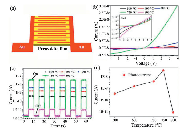
The planar architecture photodetector is used extensively in optoelectronics due to the facile fabrication and ease of integration of such structures [30]. Fig. 4a shows a schematic diagram of the perovskite device structure used here. The active layer is composed of two Schottky barriers contacting with a metal-semiconductor-metal structure [10]. Fig. 4b shows the relationship between current and voltage of perovskite devices deposited under different temperatures under illumination and the inset shows the dark current for comparison. The current increases as the deposition temperature increases. In the current device structure, the Au-perovskite interfaces are deemed to form a rectifying junction that contributes to low dark current, as can be seen from the dynamic responses of the devices in Fig. 4c. The intensity of the photocurrent increases with the deposition temperature, as shown in Fig. 4d. The highest value of the photocurrent is 3.2 × 10⁻⁸ A in the device deposited at 750 ℃. At the same time, the on/off ratio could reach 2.5 × 10⁴. This value is much higher than those for devices deposited at other temperatures. Therefore, we believe that the performance of photodetector fabricated by CVD method can be comparable with the previous works [31-34]. The superior performance of the perovskite device deposited at 750 ℃ may be attributed to the lower trap-state density, large crystalline grain size, high quality crystalline phase and fast charge carrier transfer of these perovskite films. The variation of photocurrent amplitude was not observed during the on/off cycles, verifying the reversibility and stability of the device.

|
Download:
|
| Fig. 4. The device performance of the photodetectors based on the perovskite films. (a) Schematic diagram of the device structure, (b) I-V curves of the devices under 100 mW/cm2 illumination intensity and the inset is the dark current, (c) On/off switching of the devices at a bias of 4 V, (d) photocurrent behavior of the different devices. | |
In summary, perovskite film crystalline phase was controlled by deposition temperature during the chemical vapor deposition process. The perovskite phase transfers from CsPb2Br5 (500 ℃) to CsPbBr3 (750 ℃) gradually with an increase in deposition temperature. The photophysical processes of perovskite clusters, not the gap positions, were visualized by spatially and temporally resolved spectroscopy measurements. This offers powerful evidence that the crystallinity and morphology of the perovskite films play an important role on the carrier dynamic process. The perovskite device formed by deposition at 750 ℃ shows a high photocurrent and on/off ratio reaching 2.5 × 10⁴. Our observations may offer guidelines for other perovskite film growth such as perovskites without lead ions, low dimensional perovskites and dual phase perovskites, with tunable optical, electronic and crystalline properties.
Declaration of competing interestsThe authors declare that they have no known competing financial interests or personal relationships that could have appeared to influence the work reported in this paper.
AcknowledgmentsThis work was supported by the National Natural Science Foundation of China (Nos. 61804015, 11574181), Natural Science Foundation of Jiangsu Province (No. BK20180181), the Natural Science Foundation of Jiangsu Higher Education (No. 17KJB140001). We also acknowledge support from the ARC Centre of Excellence in Exciton Science (No. CE170100026).
Appendix A. Supplementary dataSupplementarymaterial related to this article canbefound, in the online version, at doi:https://doi.org/10.1016/j.cclet.2020.05.017.
| [1] |
Y. Hou, E. Aydin, M.D. Bastiani, et al., Science 367 (2020) 1135-1140. DOI:10.1126/science.aaz3691 |
| [2] |
Y. Wang, M.I. Dar, L.K. Ono, et al., Science 365 (2019) 591-595. DOI:10.1126/science.aav8680 |
| [3] |
R. Wang, J. Xue, K.L. Wang, et al., Science 366 (2019) 1509-1513. DOI:10.1126/science.aay9698 |
| [4] |
E.H. Jung, N.J. Jeon, E.Y. Park, et al., Nature 567 (2019) 511-515. DOI:10.1038/s41586-019-1036-3 |
| [5] |
G. Huang, Y. Huang, W. Xu, et al., Chin. Chem. Lett. 30 (2020) 1021-1023. |
| [6] |
P. Wang, X. Zhang, Y. Zhou, et al., Nat. Commun. 9 (2018) 2225-2231. DOI:10.1038/s41467-018-04636-4 |
| [7] |
T. Matsushima, F. Bencheikh, T. Komino, et al., Nature 572 (2019) 502-506. DOI:10.1038/s41586-019-1435-5 |
| [8] |
W.L. Xu, M.S. Niu, X.Y. Yang, et al., Org. Electronics 48 (2017) 106-111. DOI:10.1016/j.orgel.2017.05.047 |
| [9] |
B. Yang, F. Zhang, J. Chen, et al., Adv. Mater. 29 (2017) 1703758. DOI:10.1002/adma.201703758 |
| [10] |
E. Bi, H. Chen, F. Xie, et al., Nat. Commun. 8 (2017) 15330-15336. DOI:10.1038/ncomms15330 |
| [11] |
J. Liang, J. Liu, Z. Jin, Solar RRL 1 (2017) 1700086. DOI:10.1002/solr.201700086 |
| [12] |
J. Liang, P. Zhao, C. Wang, et al., J. Am. Chem. Soc. 139 (2017) 14009-14012. DOI:10.1021/jacs.7b07949 |
| [13] |
C. Wu, Y. Zou, T. Wu, et al., Adv. Funct. Mater. 27 (2017) 1700338. DOI:10.1002/adfm.201700338 |
| [14] |
P. Ramasamy, D.H. Lim, B. Kim, et al., Chem. Commun. (Camb.) 52 (2016) 2067-2070. DOI:10.1039/C5CC08643D |
| [15] |
J. Li, L. Xu, T. Wang, et al., Adv. Mater. 29 (2017) 1603885. DOI:10.1002/adma.201603885 |
| [16] |
Z. Shi, Y. Li, Y. Zhang, et al., Nano Lett. 17 (2017) 313-321. DOI:10.1021/acs.nanolett.6b04116 |
| [17] |
M.R. Leyden, Y. Jiang, Y. Qi, J. Mater. Chem. A Mater. Energy Sustain. 4 (2016) 13125-13132. DOI:10.1039/C6TA04267H |
| [18] |
P.S. Shen, J.S. Chen, Y.H. Chiang, et al., Adv. Mater. Sci. Eng. Int. J. 3 (2016) 1500849. |
| [19] |
M.R. Leyden, L. Meng, Y. Jiang, et al., J. Phys. Chem. Lett. 8 (2017) 3193-3198. DOI:10.1021/acs.jpclett.7b01093 |
| [20] |
W. Du, S. Zhang, J. Shi, et al., ACS Photonics 5 (2018) 2051-2059. DOI:10.1021/acsphotonics.7b01593 |
| [21] |
Z. Wu, J. Chen, Y. Mi, et al., Adv. Opt. Mater. 6 (2018) 1800674. DOI:10.1002/adom.201800674 |
| [22] |
Z. Zheng, X. Wang, Y. Shen, et al., Adv. Opt. Mater. 6 (2018) 1800879. DOI:10.1002/adom.201800879 |
| [23] |
G. Tong, X. Geng, Y. Yu, et al., RSC Adv. 7 (2017) 18224-18230. DOI:10.1039/C7RA01430A |
| [24] |
J. Kim, H.P. Kim, M.A.M. Teridi, A.B. Yusoff, J. Jang, Sci. Rep. 6 (2016) 37378. DOI:10.1038/srep37378 |
| [25] |
X.T. Hao, L.J. McKimmie, T.A. Smith, J. Phys. Chem. Lett. 2 (2011) 1520-1525. DOI:10.1021/jz200540j |
| [26] |
Z. Guo, J.S. Manser, Y. Wan, P.V. Kamat, L. Huang, Nat. Commun. 6 (2015) 7471. DOI:10.1038/ncomms8471 |
| [27] |
C.T.O. Wong, S.S. Lo, L. Huang, J. Phys. Chem. Lett. 3 (2012) 879-884. DOI:10.1021/jz300178g |
| [28] |
W.L. Xu, M. Niu, X. Yang, et al., J. Phys. Chem. C 121 (2017) 26250-26255. DOI:10.1021/acs.jpcc.7b09844 |
| [29] |
D. Shi, V. Adinolfi, R. Comin, et al., Science 347 (2015) 519-522. DOI:10.1126/science.aaa2725 |
| [30] |
M.I. Saidaminov, V. Adinolfi, R. Comin, et al., Nat. Commun. 6 (2015) 8724. DOI:10.1038/ncomms9724 |
| [31] |
P. Zhang, G. Zhang, L. Liu, et al., J. Phys. Chem. Lett. 9 (2018) 5040-5046. DOI:10.1021/acs.jpclett.8b01945 |
| [32] |
M.I. Saidaminov, M.Z. Haque, J. Almutlaq, et al., Adv. Opt. Mater. 5 (2017) 1600704. DOI:10.1002/adom.201600704 |
| [33] |
J. Song, Q. Cui, J. Li, et al., Adv. Opt. Mater. 5 (2017) 1700157. DOI:10.1002/adom.201700157 |
| [34] |
J. Ding, S. Du, Z. Zuo, et al., J. Phys. Chem. C 121 (2017) 4913-4923. |