 2021, Vol. 32


b NRC (Nanostructure Research Centre), Wuhan University of Technology, Wuhan 430070, China;
c Center for Nanophase Materials Sciences, Oak Ridge National Laboratory, Oak Ridge, TN 37831, United States;
d EMAT (Electron Microscopy for Materials Science), University of Antwerp, Antwerp, B-2020, Belgium
Two-dimensional (2D) transition metal carbides, nitrides and carbonitrides, namely MXenes, were first discovered in 2011 [1] and soon grew into a new, large family of functional 2D materials. MXenes are generally prepared by selectively etching of the A-element in a layered MAX phase, where M is an early transition metal, A is a group element, and X represents C and/or N. After etching and subsequent exfoliation, the MXenes flakes are terminated by functional groups (Tx) such as —OH and —O [2, 3]. MXenes are generally conductive and hydrophilic [4-10] and have wide applications such as in catalysts [11-13], electromagnetic shielding [14, 15], supercapacitors [3, 16, 17], sensors [18], batteries [19-23] and water purification [24, 25].
Atomic defects involving missing, replacement or interstitial occupancy of an atom can be found in all the materials, and they are much smaller than other defects such as line defects, planar defects and pores. It has been shown that other 2D materials such as transition metal dichalcogenides (TMDs) exhibit a collection of interesting atomic defects that directly influence the electronic [19-23], magnetic [26] and catalytic [11-13] properties. In MXenes, the C/N (X) atoms occupy the interstitial sites of the metal (M) atom octahedrons [27], and atomic defects can form at both X site and M site. Compared to other 2D materials, MXenes have unique surface functional groups that interact with defects, which complicates the structure-property relationship and provides an additional path to enhance the properties [28]. Surface terminations are functional groups such as —OH, —F and —O that pre-exist in the etching solution, and can directly influence formation energy and concentration of atomic defects in the surface layers. Understanding the defect structure, the interaction between defects and surface terminations, the evolution and dynamics of defects under different conditions (such as temperature and time) is important for the development of MXenes with the desired properties.
The synthesis, properties and applications of MXenes have been previously reviewed [2, 12, 18, 29, 30]. The review here mainly focuses on atomic defects in MXenes. As atomic defects heavily interacts with surface functional groups in various ways, we extend our discussion to include surface functional groups. We first discuss recent progress in the research of atomic defects and surface functional groups in MXenes using scanning transmission electron microscopy (STEM) and density functional theory (DFT), neutron diffraction [31], and spectroscopy techniques [32-35]. We then focus on how the atomic defects and surface functiona groups can be controlled through synthesis and post-treatment methods, and how the atomic defects and surface functional groups in MXenes can directly influence various properties such as electron transport, Li+ adsorption, hydrogen evolution reaction (HER) activity, and magnetism. We also show that atomic defects are heavily involved in dynamic structural transformations such as oxidation and layer-by-layer growth. The growing interest in atomic defects research in MXenes will help understand structure-property relationship of MXenes and design MXenes with desired properties for different applications.
2. Atomic defects and functional groups in 2D MXenes 2.1. Experimental observation of atomic defects in MXenesDefects in 2D materials can be experimentally explored using characterization techniques such as X-ray photoelectron spectroscopy (XPS) [36, 37], scanning tunneling microscopy (STM) [38], scanning probe microscopy (SPM) [39] and STEM [40-42]. Among all these techniques, the STEM technique has the advantage of high-spatial resolution (down to 50 pm when equipped with a probe spherical aberration corrector) and the straightforward interpretation of image contrast that scales with the atomic number, namely Z contrast imaging [43-47]. Additionally, the STEM mode enables atomic resolution chemical analysis such as X-ray energy dispersive spectroscopy (EDS) and electron energy loss spectroscopy (EELS) [48, 49]. The unique capabilities of STEM make it an ideal platform to investigate atomic defects and functional groups in MXenes. Recently, STEM has been successfully used to directly reveal atomic defects in other 2D materials such as graphene [41], MoS2 [50], h-BN [51], and showed how defects can mediate electrical [50, 52], magnetic [53] and optoelectronic properties [54]. However, the detailed analysis of atomic defects in MXenes was very difficult until Alhabeb et al. developed the minimally intensive layer delamination (MILD) method that allowed for consistent synthesizable, large high-quantity single layer Ti3C2 MXene flakes with a low concentration of defects [55, 56]. Instead of HF as an etchant, a LiF and HCl solution was used as the etchant in the MILD method [56]. The single layer MXene flakes from the MILD method are ideal for the characterization of atomic defects and functional groups using STEM.
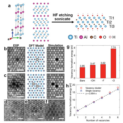
Using STEM, cation defects such as vacancies and adatoms have been analyzed in MXenes such as Ti3C2Tx [32, 57], Mo1.33C [58], W1.33C [59] and Nb2CTx [60]. For example, the atomic structure and defect structure of Ti3C2Tx MXene prepared by the MILD method has been investigated using STEM experiments performed on a Cs-corrected Nion UltraSTEM operated at 60 kV [32]. A single layer of Ti3C2Tx MXene contains five atomic layers Ti—C—Ti—C—Ti with the twoTi surfaces terminated by functional groups Tx (Fig. 1a). The single layer nature of the MXene flakes was confirmed using multiple STEM images acquired from different orientations and STEM image simulation. Atomic resolution STEM images combined with DFT simulation demonstrates that the most prevalent atomic defects that can be experimentally observed in Ti3C2Tx MXene are Ti vacancies (VTi) and VTi clusters (Fig. 1). VTi is mainly formed in the two surface Ti layers during the delamination process. It is also worth noting that cation adatoms on the surfaces of flakes are commonly found in MXenes [57, 60]. For example, surface absorption during etching and exfoliation creates abundant Nb adatoms at hcp sites on the surface of Nb2CTx MXene [60].

|
Download:
|
| Fig. 1. Atomic scale HAADF-STEM images of defects in single-layer Ti3C2Tx. (a) Crystal structure model of Ti3AlC2 (left), Ti3AlC2 projected along the a axis (middle), and MXene phase Ti3C2Tx projected along the a axis (right) with —OH terminated functional groups. (b) Comparison between experimental HAADF-STEM image, DFT model, and simulated HAADF-STEM image of VTi and (c) two adjacent VTi within the same sublayer. (d–f) Experimental HAADF-STEM images of vacancy clusters: two adjacent VTi forming within two different sublayers (d), three VTi within the same sublayer (e), and 17 VTi within the same sublayer (f). Scale bars are 0.5 nm. (g) VTi formation energy on bare Ti3C2 and terminated single-layer Ti3C2Tx. (h) Formation energy of VTi clusters as a function of number of VTi. Reprint with permission [32]. Copyright 2016, American Chemical Society. | |
DFT simulation has been widely used to calculate formation energy of atomic defects in MXenes, which provides essential information to predict which atomic defects are more likely to exist [26, 61-63]. Fig. 1h shows that the formation energy of VTi clusters scales with the vacancy number, indicating that VTi clusters can form without requiring extra energy [32]. Moreover, DFT simulation can shed lights on atomic defects of anions (C/N atoms) in MXenes, which generally exhibit a negligible contrast in STEM images as the metal atoms are much heavier than the C/N atoms. DFT simulations reveal that carbon vacancies (VC) should also exist in MXenes. First-principle calculations confirm that the formation energy of VC (from 0.6 eV to 2.7 eV) in Ti2CT2 MXene is lower than in other 2D materials such as graphene (7.4 eV) [64], while the migration energy of VC is higher [61]. Therefore, Ti2CT2 MXene with VC are thermodynamically and kinetically more stable, and should not show any structural reconstruction at the ground state and ambient temperature. Other studies show that the metal vacancies (VM) in different monolayer M2C MXenes (M = Sc, Ti, V, Zr, Nb, Mo, Hf, Ta, W) and transition metal carbides have a higher formation energy than VC [62, 63]. It was reported that X defects are more likely to form than M defects during the synthesis of the M2XO2 family MXenes (M = V, Mn, Ta and Re, X = C/N) because of the strong M—O bonds [26].
2.3. Surface functional group of 2D MXenesTo ensure surface charge neutrality, MXenes surfaces are always covered by functional groups (Fig. 1a) such as —O, —OH and —F, which significantly impact surface electrochemical properties [33, 65, 66]. The surface functional groups alter the formation energy of atomic defects. For example, DFT calculation confirms that the formation energy of VTi is the highest when the surface is —O terminated (Fig. 1g), implying modifying functional groups can change VTi concentration. The formation energy of VTi in Ti2XO2 is higher than in Ti2XF2 and Ti2X(OH)2 due to a stronger Ti-O bond in Ti2XO2 [26]. Surface functional groups can be characterized using various experimental techniques such as EDS, nuclear magnetic resonance (NMR) spectroscopy [34, 67], neutron diffraction [31] and STEM-EELS [57]. NMR revealed that the surface termination depends on the synthesis method. MXenes etched by a LiF-HCl solution has four times less —F groups than MXenes etched by HF [67]. NMR confirmed the connectivity of termination by directly measuring the polarization transferred from the —OH surface termination to the center of the V2CTx MXene [34]. Neutron scattering was used to understand two types of layer-layer interactions and interlayer bonding formation, including van der Waals forces between layers and hydrogen bonds of functional groups between layers [31]. Monte Carlo (MC) simulations confirmed that the distribution of —O, —OH, and —F functional groups on Ti-based MXene surface are related to experimental parameters such as of the etching solution pH value, etching temperature, and work function [68]. Cs-corrected STEM-EELS has been utilized to investigate the chemical and structural characteristics of the surface groups in Ti3C2Tx MXene at atomic resolution, which confirms the non-uniform coverage of O-based surface groups [57]. Combining STEM experiment and simulation, it is possible to determine whether the function group occupies the top, the bottom or both surfaces of the flake (Fig. 2) [35].

|
Download:
|
| Fig. 2. False color STEM intensity patterns. (a) Bare Ti3C2 surface; (b) O adatoms occupying A-sites on the bottom MXene surface; (c) O adatoms on A-sites on top surface; (d) O adatoms occupying A-sites on both top and bottom surfaces. Insets show correlated STEM simulation of respective surfaces. Scale bar 0.5 nm. Reprint with permission [35]. Copyright 2018, IOP Publishing. | |
Controlling the type and concentration of atomic defects in 2D materials to enhance properties has been extensively explored for graphene [69] and 2D TMDs [53, 70]. In this section we will summarize the recent progress in how to control atomic defects and surface functional groups through synthesizing methods, and how atomic defects and surface functional groups can eventually influence the properties of MXenes.
3.1. Tuning atomic defects and functional groupsAs MXenes are generally synthesized through the selective etching of the MAX phase [1, 28], etching parameters can directly affect atomic defects in MXenes. A systematic investigation of atomic defects in monolayer Ti3C2Tx MXene, prepared by the MILD method with different equivalent HF concentration (2.7 wt%, 5.3 wt%, and 7.0 wt%), indicates that the average defect concentration increases as the HF concentration increases (Fig. S1 in Supporting information) [32]. Moreover, the higher HF concentration facilitates the formation of VTi clusters, while isolated VTi are more commonly observed when a lower HF concentration was used. Altering the HF concentration thus provides a facile way to control atomic defects in Ti3C2Tx MXene. Molecular dynamics simulations show that the surface functional groups in the vicinity of VTi defects tend to detach from the surface and expose Ti atoms at the central layer as active sites for potential catalytic applications. DFT suggests that VTi defects in the Ti surface layers do not deteriorate the electrical properties, consistent with the model that electrons mainly transport through the central layer [32]. Another example is selective etching of both Al and Sc atoms in the MAX phase (Mo2/3Sc1/3)2AlC with in-plane chemical ordering to create 2D Mo1.33C MXene with periodic cation divacancies [58].
Electron irradiation has been used to engineer the structure of materials such as low-dimensional materials [71] and nanostructured carbon materials [72]. Electron irradiation therefore provides a new route to tune the atomic defect concentration [73]. Zhang et al. [73] found that high-energy electron irradiation knocks Ti atoms out to the surface and creates VTi in the outer Ti layer because the formation energies of VTi in the outer layer is lower than in the inner layer in Ti3C2 flakes. Comparison between experimental and simulated STEM images confirms that the relative intensity of the functional groups increases as more Ti vacancies are formed by electron beam irradiation (Fig. S2 in Supporting information). DFT calculations indicate that the atomic repartition could decrease the anisotropy and increase the conductivity [73].
Removal or replacement of surface function groups could be achieved using heating at different temperatures and atmospheres [74]. When using an HF-based etchant, the MXenes surface is mainly occupied by —OH functional groups, which could be removed via high-temperature annealing in vacuum as confirmed by STEM-EELS [8]. Using the same method, the surface functional groups —OH in Ti3C2F2OH can be replaced by —O at 473–1073 K, and the —O terminations of Ti3C2F2O0.5 are more likely to detach than —F above 1073 K in Ar atmosphere [74].
3.2. The influence of atomic defects on functional propertiesThe combined atomic defects and surface functional groups influence various properties of MXenes. For example, although the designed ordered structure of W vacancies renders W1.33C MXene a potentially versatile and promising layered catalyst, its HER activity is greatly compromised by surface functional groups —O/OH (Fig. 3). After annealing in a forming gas (3% hydrogen and 97% argon gas) for 1 h at 700 ℃, the surface —O/OH coverage is greatly reduced and a significant increase in HER activity was obtained [59]. Cheng et al. [75] showed that the low concentration of VC defects in Cr2CO2 MXene weakens the binding strength of the H atom with the surface of Cr2CO2, which increases the HER performance. Similarly, the HER performance of the g-C3N4/Ti3C2 composite annealed in air with more —O functional groups increases by 105% compared to annealing in N2, due to the increase in the separation of the electron-hole pairs [76].

|
Download:
|
| Fig. 3. (a–c) Top view of HAADF-STEM of single W1.33C sheets with ordered divacancies obtained from parent (W2/3Sc1/3)2AlC. (a) Low-magnification image of single flake. (b) Higher magnification image with corresponding FFT (shown in inset). (c) Atomically resolved image with overlaid schematic atomic structure model. (d) HER polarization curves for Mo1.33C (green), unannealed W1.33C (dashed red), annealed W1.33C (red), and Pt/C (black) recorded in H2 saturated 0.1 mol/L HClO4 at room temperature. Reprint with permission [59]. Copyright 2018, John Wiley and Sons. | |
Defects and surface functional groups also significantly influence the lithium ion battery (LIB) performance of MXenes. For example, VM acts as a potential trap that can improve the Li+ adsorption, which could partially be the reason for the first cycle irreversibility of Mo2C MXene LIBs [62]. First-principle calculations were used to investigate the effect of different vacancies on the diffusion and adsorption of Li atoms in the monolayer Ti2C and Ti2CT2 (T = —F or —OH) system, where both VC and VTi could improve the adsorption of Li+ ions with the presence of functional groups [77]. In addition, the adsorption energies and diffusion barriers of Li+ on pristine and defective monolayer Ti2C and Ti2CT2 were calculated by Wan et al. [77]. Without defects, Li+ ions are more difficult to bond on the surface of monolayer Ti2C(OH)2 than on bare surfaces of monolayers Ti2C and Ti2CF2·VC enhances the Li+ adsorption on monolayer Ti2C while VTi improves the Li+ adsorption on monolayers Ti2C(OH)2 and Ti2CF2 (Fig. S3 in Supporting information). Surface terminations also impact the Li+ storage capacity of MXenes. For example, MXenes with —O functional groups have the highest capacity due to the lower absorption energies and intensive interaction between Li and —O [8].
Intrinsic defects in MXenes could induce magnetism due to spin split of d-orbitals [26]. DFT predicts that O-vacancy-line (OVL) defects can form defective armchair-edged Ti2CO2 nanoribbon structures with significant magnetism [78]. The different positions of OVL could regulate the carrier mobility, carrier polarity and spin polarity. Atomic defects in MXenes can also influence the electronic properties, causing a metal-semiconductor transition [26]. Defective Ti2CO2 becomes metallic because of a Fermi energy shift upward or downward caused by VC or VTi [79].
4. Defects-induced oxidation and growth 4.1. Influence of defects on the oxidation of MXenesAtomic defects play an important role in the oxidation of MXenes flakes, which is the critical factor that leads to degradation of MXene-based devices. The experimental results show that Ti3C2Tx MXene flakes in water solution are completely oxidized after 15 days at room temperature (RT) in air. Ar gas and lower temperature (4 ℃) can reduce the oxidation rate by 98.8% [80]. In-situ TEM shows that TiO2 rutile nanoparticles are obtained at slow heating rate, while TiO2 anatase nanoparticles are formed at rapid heating rate through the flash oxidation method [81]. Using STEM, Xia et al. [82] suggested that ambient degradation of Ti3C2 MXene starts from atomic defects in Ti3C2 MXene flakes. VTi defects with a positive charge induce the formation of amorphous carbon, while the extra Ti cations can react with O2 at the defective surface of Ti3C2 to form TiO2 (Fig. S4 in Supporting information).
It is worth noting that the oxidation provides new ways to synthesize transition metal oxide nanoparticles [83] to form composite materials such as the Nb2O5/C/Nb2C composite [84] and TiO2/Ti3C2 nanocomposites with excellent photocatalytic properties [85]. MXenes (Ti3C2Tx, Nb2CTx and Ti2CTx) with TiO2 show an improvement in hydrogen production as photocatalysts [86]. In addition to oxidation, nitriding-pretreatment provides another way to control the atomic defects such as in Ti3C2Tx MXene. The engineering superstructure of the N-remedying MXenes displays eminent separation ability of photogenerated carriers and excellent light-absorption properties. Without any cocatalyst, it shows an efficient photocatalytic performance in water-splitting under visible light [87].
4.2. Defects assisted homoepitaxial growth in MXenesAtomic defects play key roles in bottom-up growth of 2D materials. Although at least 70 different MXenes have been reported from experiment or theory [2], all of them have been synthesized via top-down strategies (e.g., selectively etching by HF) [30]. Xu et al. [88] used the CVD method to grow large-areas and high-quality 2D ultrathin α-Mo2C, with the thickness of a few nanometers. Centimeter-level 2D Mo2C was grown on a graphene film using a one-step molten copper-catalyzed CVD method [89]. Large-size and high-quality 2D MoN flakes were synthesized through the reduction of 2D hexagonal oxides in ammonia [90]. 2D δ-MoN nanosheets could be obtained using a two-step approach including a hot-filament CVD process and phase transformation heating in NH3 at 800 ℃ [91]. Compared to the selective etching method, these bottom-up strategies have advantages such as one-step synthesis, controllable thickness, large size and high quality [92-94]. Despite all the effort, bottom-up growth of single layer MXenes is still difficult to achieve.
Atomic defects assisted homoepitaxial Frank-van der Merwe atomic layer growth of a TiC single adlayer on the MXenes surface was revealed via in-situ heating and electronbeam irradiation in STEM [95]. After the surface functional groups are removed by heating and irradiation, Ti and C atoms around the Ti vacancies become active and migrate to the surface to form adatoms (Figs. 4a and b). The C and Ti adatoms then diffuse on the bare Ti3C2 surface and eventually form a single h-Ti layer on the bare Ti3C2 surface.

|
Download:
|
| Fig. 4. Homoepitaxial growth of MXene. (a) Schematic of the homoepitaxial growth process to form single layer h-TiC on a monolayer Ti3C2 substrate through electron-beam irradiation and heating. Ti atoms from different layers are plotted using different shades of blue. (b) Crystal structure of monolayer Ti3C2Tx viewed from [100] and [001] zone axes. (c) Atomic resolution STEM image acquired from monolayer Ti3C2Tx along the [001] zone axis at room temperature. Areas of Ti vacancies are indicated by white dotted circles. (d) A STEM image acquired after heating and electron-beam irradiating monolayer Ti3C2 flakes inside the microscope at 500 ℃. (e) A STEM image acquired after heating MXene flakes inside the microscope at 1000 ℃. Reprint with permission [95]. Copyright 2018, Nature. | |
This review summarizes recent advances on atomic defects and surface terminations in MXenes. We have shown that various atomic defects can be induced and controlled in MXenes through the etching process or post-treatment. Also, the interaction between surface functional groups and atomic defects has been reviewed. The defects and terminations in MXenes influence a wide range of properties such as electron transport, Li ion adsorption, HER activity, and magnetism; they also control dynamic processes such as oxidation and homoepitaxial growth. This review thus provides insights on how to engineer defects in MXenes in order to acquire the desired properties. Although various techniques have been employed to investigate atomic defects and surface terminations in MXenes, our understanding of their roles is still very limited. While cation vacancies have been directly observed using STEM, the role of C/N vacancies can only be investigated using theoretical calculations. The correlation between defects and properties is mostly qualitative. With the development of experimental and theoretical techniques such as four-dimensional (4D) STEM with higher spatial resolution and temporal resolution, In-situ S/TEM techniques that can directly observe the behavior of the atomic defects and surface terminations during working conditions, and theoretical models that better describe MXenes, our knowledge on MXenes will be further broadened.
Declaration of competing interestThe authors declare that they have no known competing financial interests or personal relationships that could have appeared to influence the work reported in this paper.
AcknowledgmentsThis work was supported by the National Natural Science Foundation of China (No. 51902237), the Fundamental Research Funds for the Central Universities of China (No. WUT: 2019III012GX), Nanostructure Research Center (NRC), and Center for Materials Analysis and Testing at Wuhan University of Technology. A portion of this work was supported by the Fluid Interface Reactions, Structures and Transport (FIRST) Center, an Energy Frontier Research Center funded by the U.S. Department of Energy, Office of Science, Office of Basic Energy Sciences (RRU).
Appendix A. Supplementary dataSupplementary material related to this article can be found, in the online version, at doi:https://doi.org/10.1016/j.cclet.2020.04.024.
| [1] |
M. Naguib, M. Kurtoglu, V. Presser, et al., Adv. Mater. 23 (2011) 4248-4253. DOI:10.1002/adma.201102306 |
| [2] |
B. Anasori, M.R. Lukatskaya, Y. Gogotsi, Nat. Rev. Mater. 1 (2017) 16098. |
| [3] |
R.B. Rakhi, B. Ahmed, M.N. Hedhili, D.H. Anjum, H.N. Alshareef, Chem. Mater. 27 (2015) 5314-5323. DOI:10.1021/acs.chemmater.5b01623 |
| [4] |
M. Khazaei, M. Arai, T. Sasaki, et al., Adv. Funct. Mater. 23 (2013) 2185-2192. DOI:10.1002/adfm.201202502 |
| [5] |
I. Shein, A. Ivanovskii, Comp. Mater. Sci. 65 (2012) 104-114. DOI:10.1016/j.commatsci.2012.07.011 |
| [6] |
M. Ghidiu, M.R. Lukatskaya, M.-Q. Zhao, Y. Gogotsi, M.W. Barsoum, Nature 516 (2014) 78. DOI:10.1038/nature13970 |
| [7] |
M. Khazaei, M. Arai, T. Sasaki, M. Estili, Y. Sakka, Phys. Chem. Chem. Phys. 16 (2014) 7841-7849. DOI:10.1039/C4CP00467A |
| [8] |
Y. Xie, M. Naguib, V.N. Mochalin, et al., J. Am. Chem. Soc. 136 (2014) 6385-6394. DOI:10.1021/ja501520b |
| [9] |
X. Yu, Y. Li, J. Cheng, et al., ACS Appl. Mater. Inter. 7 (2015) 13707-13713. DOI:10.1021/acsami.5b03737 |
| [10] |
M. Ashton, K. Mathew, R.G. Hennig, S.B. Sinnott, J. Phys. Chem. C 120 (2016) 3550-3556. DOI:10.1021/acs.jpcc.5b11887 |
| [11] |
T.Y. Ma, J.L. Cao, M. Jaroniec, S.Z. Qiao, Angew. Chem. Int. Ed. 55 (2016) 1138-1142. DOI:10.1002/anie.201509758 |
| [12] |
J. Zhu, E. Ha, G. Zhao, et al., Coord. Chem. Rev. 352 (2017) 306-327. DOI:10.1016/j.ccr.2017.09.012 |
| [13] |
G. Gao, A.P. O'Mullane, A. Du, ACS Catal. 7 (2016) 494-500. |
| [14] |
F. Shahzad, M. Alhabeb, C.B. Hatter, et al., Science 353 (2016) 1137-1140. DOI:10.1126/science.aag2421 |
| [15] |
J. Liu, H.B. Zhang, R. Sun, et al., Adv. Mater. 29 (2017) 1702367. DOI:10.1002/adma.201702367 |
| [16] |
C. Zhang, M.P. Kremer, A. Seral-Ascaso, et al., Adv. Funct. Mater. 28 (2018) 1705506. DOI:10.1002/adfm.201705506 |
| [17] |
M.R. Lukatskaya, O. Mashtalir, C.E. Ren, et al., Science 341 (2013) 1502-1505. DOI:10.1126/science.1241488 |
| [18] |
R.A. Soomro, S. Jawaid, Q. Zhu, Z. Abbas, B. Xu, Chin. Chem. Lett. (2019). DOI:10.1016/j.cclet.2019.12.005 |
| [19] |
Y. Xie, Y. Dall'Agnese, M. Naguib, et al., ACS Nano 8 (2014) 9606-9615. DOI:10.1021/nn503921j |
| [20] |
D. Er, J. Li, M. Naguib, Y. Gogotsi, V.B. Shenoy, ACS Appl. Mater. Inter. 6 (2014) 11173-11179. DOI:10.1021/am501144q |
| [21] |
X. Liang, A. Garsuch, L.F. Nazar, Angew. Chem. Int. Ed. 54 (2015) 3907-3911. DOI:10.1002/anie.201410174 |
| [22] |
B. Ahmed, D.H. Anjum, Y. Gogotsi, H.N. Alshareef, Nano Energy 34 (2017) 249-256. DOI:10.1016/j.nanoen.2017.02.043 |
| [23] |
M. Naguib, J. Come, B. Dyatkin, et al., Electrochem. commun. 16 (2012) 61-64. DOI:10.1016/j.elecom.2012.01.002 |
| [24] |
K. Rasool, M. Helal, A. Ali, et al., ACS Nano 10 (2016) 3674-3684. DOI:10.1021/acsnano.6b00181 |
| [25] |
Q. Zhang, J. Teng, G. Zou, et al., Nanoscale 8 (2016) 7085-7093. DOI:10.1039/C5NR09303A |
| [26] |
A. Bandyopadhyay, D. Ghosh, S.K. Pati, Phys. Chem. Chem. Phys. 20 (2018) 4012-4019. DOI:10.1039/C7CP07165E |
| [27] |
M.W. Barsoum, Prog. Solid State Chem. 28 (2000) 201-281. DOI:10.1016/S0079-6786(00)00006-6 |
| [28] |
M. Naguib, O. Mashtalir, J. Carle, et al., ACS Nano 6 (2012) 1322-1331. DOI:10.1021/nn204153h |
| [29] |
B.-M. Jun, S. Kim, J. Heo, et al., Nano Res. 12 (2019) 471-487. DOI:10.1007/s12274-018-2225-3 |
| [30] |
M. Naguib, V.N. Mochalin, M.W. Barsoum, Y. Gogotsi, Adv. Mater. 26 (2014) 992-1005. DOI:10.1002/adma.201304138 |
| [31] |
H.-W. Wang, M. Naguib, K. Page, D.J. Wesolowski, Y. Gogotsi, Chem. Mater. 28 (2016) 349-359. DOI:10.1021/acs.chemmater.5b04250 |
| [32] |
X. Sang, Y. Xie, M.-W. Lin, et al., ACS Nano 10 (2016) 9193-9200. DOI:10.1021/acsnano.6b05240 |
| [33] |
P.O. Persson, J. Rosen, Curr. Opin. Solid State Mater. Sci. 23 (2019) 100774. DOI:10.1016/j.cossms.2019.100774 |
| [34] |
K.J. Harris, M. Bugnet, M. Naguib, M.W. Barsoum, G.R. Goward, J. Phys. Chem. C 119 (2015) 13713-13720. DOI:10.1021/acs.jpcc.5b03038 |
| [35] |
I. Persson, L.-Å. Näslund, J. Halim, et al., 2D Mater 5 (2017) 015002. DOI:10.1088/2053-1583/aa89cd |
| [36] |
D. Ganta, S. Sinha, R.T. Haasch, Surf. Sci. Spectra 21 (2014) 19-27. DOI:10.1116/11.20140401 |
| [37] |
N.P. Kondekar, M.G. Boebinger, E.V. Woods, M.T. McDowell, ACS Appl. Mater. Inter. 9 (2017) 32394-32404. DOI:10.1021/acsami.7b10230 |
| [38] |
R. Addou, L. Colombo, R.M. Wallace, ACS Appl. Mater. Inter. 7 (2015) 11921-11929. DOI:10.1021/acsami.5b01778 |
| [39] |
H.I. Rasool, C. Ophus, A. Zettl, Adv. Mater. 27 (2015) 5771-5777. DOI:10.1002/adma.201500231 |
| [40] |
L. Stobinski, B. Lesiak, A. Malolepszy, et al., J. Electron. Spectrosc. Relat. Phenom. 195 (2014) 145-154. DOI:10.1016/j.elspec.2014.07.003 |
| [41] |
W. Zhou, M. Prange, M. Oxley, et al., Microsc. Microanal. 17 (2011) 1498-1499. DOI:10.1017/S1431927611008361 |
| [42] |
A. Hashimoto, K. Suenaga, A. Gloter, K. Urita, S. Iijima, Nature 430 (2004) 870-873. DOI:10.1038/nature02817 |
| [43] |
O.L. Krivanek, M.F. Chisholm, V. Nicolosi, et al., Nature 464 (2010) 571. DOI:10.1038/nature08879 |
| [44] |
M. Haider, S. Uhlemann, E. Schwan, et al., Nature 392 (1998) 768-769. DOI:10.1038/33823 |
| [45] |
D. Muller, L.F. Kourkoutis, M. Murfitt, et al., Science 319 (2008) 1073-1076. DOI:10.1126/science.1148820 |
| [46] |
G. Van Tendeloo, S. Bals, S. Van Aert, J. Verbeeck, D. Van Dyck, Adv. Mater. 24 (2012) 5655-5675. DOI:10.1002/adma.201202107 |
| [47] |
S.J. Pennycook, Ultramicroscopy 123 (2012) 28-37. DOI:10.1016/j.ultramic.2012.05.005 |
| [48] |
M. Bosman, V. Keast, J. Garcia-Munoz, et al., Phys. Rev. Lett. 99 (2007) 086102. DOI:10.1103/PhysRevLett.99.086102 |
| [49] |
A. d'Alfonso, B. Freitag, D. Klenov, Phys. Rev. B 81 (2010) 100101. DOI:10.1103/PhysRevB.81.100101 |
| [50] |
W. Zhou, X. Zou, S. Najmaei, et al., Nano Lett. 13 (2013) 2615-2622. DOI:10.1021/nl4007479 |
| [51] |
R. Bourrellier, S. Meuret, A. Tararan, et al., Nano Lett. 16 (2016) 4317-4321. DOI:10.1021/acs.nanolett.6b01368 |
| [52] |
D. Wong, J. Velasco Jr., L. Ju, et al., Nat. Nanotech. 10 (2015) 949. DOI:10.1038/nnano.2015.188 |
| [53] |
J. Hong, Z. Hu, M. Probert, et al., Nat. Commun. 6 (2015) 6293. DOI:10.1038/ncomms7293 |
| [54] |
K.F. Mak, K. He, J. Shan, T.F. Heinz, Nat. Nanotech. 7 (2012) 494. DOI:10.1038/nnano.2012.96 |
| [55] |
A. Lipatov, M. Alhabeb, M.R. Lukatskaya, et al., Adv. Electron. Mater. 2 (2016) 1600255. DOI:10.1002/aelm.201600255 |
| [56] |
M. Alhabeb, K. Maleski, B. Anasori, et al., Chem. Mater. 29 (2017) 7633-7644. DOI:10.1021/acs.chemmater.7b02847 |
| [57] |
L.H. Karlsson, J. Birch, J. Halim, M.W. Barsoum, P.O. Persson, Nano Lett. 15 (2015) 4955-4960. DOI:10.1021/acs.nanolett.5b00737 |
| [58] |
Q. Tao, M. Dahlqvist, J. Lu, et al., Nat. Commun. 8 (2017) 14949. DOI:10.1038/ncomms14949 |
| [59] |
R. Meshkian, M. Dahlqvist, J. Lu, et al., Adv. Mater. 30 (2018) 1706409. DOI:10.1002/adma.201706409 |
| [60] |
J. Palisaitis, I. Persson, J. Halim, J. Rosen, P.O. Persson, Nanoscale 10 (2018) 10850-10855. DOI:10.1039/C8NR01986J |
| [61] |
T. Hu, J. Yang, X. Wang, Phys. Chem. Chem. Phys. 19 (2017) 31773-31780. DOI:10.1039/C7CP06593K |
| [62] |
H. Wu, Z. Guo, J. Zhou, Z. Sun, Appl. Surf. Sci. 488 (2019) 578-585. DOI:10.1016/j.apsusc.2019.05.311 |
| [63] |
X.X. Yu, G.B. Thompson, C.R. Weinberger, J. Eur. Ceram. Soc. 35 (2015) 95-103. DOI:10.1016/j.jeurceramsoc.2014.08.021 |
| [64] |
A. El-Barbary, R. Telling, C. Ewels, M. Heggie, P. Briddon, Phys. Rev. B 68 (2003) 144107. DOI:10.1103/PhysRevB.68.144107 |
| [65] |
Q. Tang, Z. Zhou, P. Shen, J. Am. Chem. Soc. 134 (2012) 16909-16916. DOI:10.1021/ja308463r |
| [66] |
J.L. Hart, K. Hantanasirisakul, A.C. Lang, et al., Nat. Commun. 10 (2019) 1-10. DOI:10.1038/s41467-018-07882-8 |
| [67] |
M.A. Hope, A.C. Forse, K.J. Griffith, et al., Phys. Chem. Chem. Phys. 18 (2016) 5099-5102. DOI:10.1039/C6CP00330C |
| [68] |
R. Ibragimova, M.J. Puska, H.P. Komsa, ACS Nano 13 (2019) 9171-9181. DOI:10.1021/acsnano.9b03511 |
| [69] |
L. Vicarelli, S.J. Heerema, C. Dekker, H.W. Zandbergen, ACS Nano 9 (2015) 3428-3435. DOI:10.1021/acsnano.5b01762 |
| [70] |
X. Sang, X. Li, W. Zhao, et al., Nat. Commun. 9 (2018) 2051. DOI:10.1038/s41467-018-04435-x |
| [71] |
T. Susi, J.C. Meyer, J. Kotakoski, Ultramicroscopy 180 (2017) 163-172. DOI:10.1016/j.ultramic.2017.03.005 |
| [72] |
A. Krasheninnikov, F. Banhart, Nat. Mater. 6 (2007) 723-733. DOI:10.1038/nmat1996 |
| [73] |
H. Zhang, T. Hu, W. Sun, et al., Chem. Mater. 31 (2019) 4385-4391. DOI:10.1021/acs.chemmater.9b00470 |
| [74] |
Z. Li, L. Wang, D. Sun, et al., Mater. Sci. Eng. B 191 (2015) 33-40. DOI:10.1016/j.mseb.2014.10.009 |
| [75] |
Y.W. Cheng, J.H. Dai, Y.M. Zhang, Y. Song, J. Mater. Chem. A 6 (2018) 20956-20965. DOI:10.1039/C8TA07749E |
| [76] |
Y. Sun, D. Jin, Y. Sun, et al., J. Mater. Chem. A 6 (2018) 9124-9131. DOI:10.1039/C8TA02706D |
| [77] |
Q. Wan, S. Li, J.B. Liu, ACS Appl. Mater. Inter. 10 (2018) 6369-6377. DOI:10.1021/acsami.7b18369 |
| [78] |
R. Hu, Y. Li, Z. Zhang, Z. Fan, L. Sun, J. Mater. Chem. C 7 (2019) 7745-7759. |
| [79] |
C. Wang, H. Han, Y. Guo, Comp. Mater. Sci. 159 (2019) 127-135. DOI:10.1016/j.commatsci.2018.12.007 |
| [80] |
C.J. Zhang, S. Pinilla, N. McEvoy, et al., Chem. Mater. 29 (2017) 4848-4856. DOI:10.1021/acs.chemmater.7b00745 |
| [81] |
H. Ghassemi, W. Harlow, O. Mashtalir, et al., J. Mater. Chem. A 2 (2014) 14339-14343. DOI:10.1039/C4TA02583K |
| [82] |
F. Xia, J. Lao, R. Yu, et al., Nanoscale 11 (2019) 23330-23337. DOI:10.1039/C9NR07236E |
| [83] |
G. Deysher, S. Sin, Y. Gogotsi, B. Anasori, Mater. Today 21 (2018) 1064-1065. DOI:10.1016/j.mattod.2018.10.035 |
| [84] |
T. Su, R. Peng, Z.D. Hood, et al., ChemSusChem 11 (2018) 688-699. DOI:10.1002/cssc.201702317 |
| [85] |
Y. Gao, L. Wang, A. Zhou, et al., Mater. Lett. 150 (2015) 62-64. DOI:10.1016/j.matlet.2015.02.135 |
| [86] |
H. Wang, R. Peng, Z.D. Hood, et al., ChemSusChem 9 (2016) 1490-1497. DOI:10.1002/cssc.201600165 |
| [87] |
X. Kong, P. Gao, R. Jiang, et al., Appl. Catal. A: Gen. 590 (2020) 117341. DOI:10.1016/j.apcata.2019.117341 |
| [88] |
C. Xu, L. Wang, Z. Liu, et al., Nat. Mater. 14 (2015) 1135. DOI:10.1038/nmat4374 |
| [89] |
D. Geng, X. Zhao, Z. Chen, et al., Adv. Mater. 29 (2017) 1700072. DOI:10.1002/adma.201700072 |
| [90] |
X. Xiao, H. Yu, H. Jin, et al., ACS Nano 11 (2017) 2180-2186. DOI:10.1021/acsnano.6b08534 |
| [91] |
S. Joshi, Q. Wang, A. Puntambekar, V. Chakrapani, ACS Energy Lett. 2 (2017) 1257-1262. DOI:10.1021/acsenergylett.7b00240 |
| [92] |
H.-U. Krebs, M. Weisheit, J. Faupel, et al., Pulsed laser deposition (PLD)-a versatile thin film technique, in: B. Kramer (Ed. ), Advances in Solid State Physics, Springer, Berlin, Heidelberg, 2003, pp. 505-518.
|
| [93] |
L. Verger, C. Xu, V. Natu, et al., Curr. Opin. Solid State Mater. Sci. 23 (2019) 149-163. DOI:10.1016/j.cossms.2019.02.001 |
| [94] |
Z. Zhang, F. Zhang, H. Wang, et al., J. Mater. Chem. C 5 (2017) 10822-10827. DOI:10.1039/C7TC03652C |
| [95] |
X. Sang, Y. Xie, D.E. Yilmaz, et al., Nat. Commun. 9 (2018) 2266. DOI:10.1038/s41467-018-04610-0 |