 2020, Vol. 31


b Laboratory of Theoretical and Computational Chemistry, Institute of Theoretical Chemistry and College of Chemistry, Jilin University, Changchun 130023, China;
c Beijing National Laboratory for Molecular Sciences(BNLMS), Beijing 100190, China
Two-dimensional materials such as graphene [1, 2], h-BN [3, 4], carbon nitride [5-7] and transition metal dichalcogenides (TMD) [8-11] have been widely investigated in recent years because of their superb properties and application in photoelectric fields. According to recent reports, heterostructures constructed with different 2D materials through van der Waals interaction could produce new electronic structures, which results in their electronic or optoelectronic properties surpass those of the individual 2D materials [12-14]. For example, the calculated small band gaps are opened at the Dirac points of graphene and silene in hybrid G/S heterostructure [15] and the self-doping way is tuned by interlayer distance in G/S heterostructure. Smaller band gap than each individual monolayer appears and can be tuned by the distance between two layers in BP/g-GeC vdW heterostructure [16]. Electron-hole pair separation and high photoabsorption performance can be realized in MoS2/ZnO vdW heterostructure [17]. Black phosphorus stacked on GeC shows promising potential as a visible-light photocatalyst for its smaller and tunable band gap [16].
Both moderate electronic band gap and effective photoinduced electron-hole pair separation are indispensable factors for application of semiconductor in photocatalytic CO2 reduction reaction [18-20]. Recent works have demonstrated that a new 2D semiconducting materials with a direct band gap, namely, the covalent organic framework C4N (C4N-COF), have been successfully synthesized through hydrothermal solvent method [21]. C4N with distributed hexagonal pores and C, N stoichiometry (4:1) possesses ordered crystalline structure and exhibits excellent electrocatalysis. It possesses a suitable band gap which is lower than the minimum visible-light energy and reaction active sites for OER, which makes C4N a potential candidate for applications in visible photocatalytic CO2 reduction reaction (CO2RR).
Meanwhile, to design a new effective heterostructure for photocatalytic CO2RR as an efficient photocatalyst, researchers recently start focusing on vdW heterostructure based on COFs and TMDs [22-25]. It is well known that vdW heterostructure utilize the characteristics of constituent 2D materials leaving their electronic properties unaffected to a large extent. Depending on the relative positions of band edges of the two constituent 2D layers, different types of heterojunctions can be formed. Among them, type-Ⅱ heterostructures are promising for attaining smaller band gap and efficient charge separation because the valence-band maximum (VBM) and conduction-band minimum (CBM) appears in different layers. Therefore, when the photogenerated electronhole pairs split at the interface, the electrons would transfer from a material to another and the holes would transfer in the opposite direction. This phenomenon makes type-Ⅱ heterostructures very suitable for application in photocatalytic reaction.
MoS2 is a typical TMD which has a direct bandgap and is a potential photocatalyst for CO2 reduction [26-28]. However, the recombination rate of photogenerated electron–hole pairs in MoS2 monolayer is high [27, 29, 30], which affect its photocatalysis seriously. It is reported that g-C3N4/MoS2 nanocomposite [31] forms a type-Ⅱ band alignment resulting the charge transfer between MoS2 and g-C3N4 and leads to the high hydrogenevolution reaction activity. Kumar et al. demonstrated that C2N/ WS2 vdW heterostructure shows high charge carrier mobility, indicating their efficient utilization in reduction and oxidation reactions [32]. Moreover, C2N/WS2 vdW heterostructure has absorption coefficient of 2.98 × 105 cm-1 in the visible light region which ensured that it is an efficient visible light harvesting photocatalyst. Hence, C4N-COF stacked on MoS2 monolayer to form a C4N/MoS2 vdW heterostructure is undoubtedly a new and efficient photocatalyst for CO2RR.
In this work, we studied the geometric stability, electronic and optical properties of the C4N/MoS2 heterostructure by using first principle calculations. We concentrated on the basic mechanism of the interfacial coupling effect and charge transfer and separation in the C4N/MoS2 heterostructure. Our calculations reveal that after forming the C4N/MoS2 heterostructure, the bandgap and the band edge positions of C4N and MoS2 will change correspondingly because of the interlayer interaction of the C4N/MoS2 interlayer. The type-Ⅱ band alignment and the difference of work function indicates that a built-in electric field is formed within the heterostructure. The built-in electric field could separate the photogenerated electrons and holes which produce the active sites for photocatalytic CO2 reduction reaction. Furthermore, we found that the optical absorption coefficient of the C4N/MoS2 heterostructure is higher than those of individual C4N and MoS2 under visible-light irradiation. In the paper, we take volumes to describe for understanding the interlayer properties and especially the detailed interfacial properties of the C4N/MoS2 heterostructure.
All calculations were performed using density functional theory, as implemented in the Vienna Ab initio Simulation Package (VASP) [33, 34] with the projector augmented wave (PAW) method [35]. Compared with other functionals, we also tested the calculation with and without spin-orbital coupling (SOC) correction. Finally, the exchange and correlation potential were described with the Perdew-Burke-Ernzerhof (PBE) [36] of the generalized gradient approximation (GGA) [37, 38]. Due to the absence of strong bonding interactions between C4N and MoS2, weak van der Waals interactions are expected to play a large role. We adopted a DFT-D2 method proposed by Grimme to describe vdW interactions correctly. All force field parameters are obtained based on the PBE functional, as given in the literature [39]. The total energy (ETotal) is represented as:
|
Where EKS-DFT is the conventional Kohn-Sham DFT energy and Evdw is the dispersion correction. The energy cutoff is set to be 520 eV and a Γ-centered mesh of 4 × 4×1 k-points is used to sample the structure optimizations and total energy calculations of the C4N/ MoS2 heterostructure, respectively. All calculations are fully converged. Geometry optimizations were terminated when the energy and force on each ion were reduced below 10-5 eV per atom and 0.01 eV/Å, and the optimized structures were then used to calculate the structural, electronic and optical properties.
To explore the optical properties of the C4N/MoS2 heterostructure, the optical absorption spectra are simulated by converting the complex dielectric function to the absorption coefficient αabs according to the following relation [40]:

|
Where ε1(ω) and ε2(ω) are the real and imaginary parts of the frequency dependent complex dielectric function ε(ω). Taking into account the tensor nature of the dielectric function, ε1(ω) and ε2(ω) are averaged over three polarization vectors.
Before investigating the electronic properties of the C4N/MoS2 heterostructure, the crystal structures of the C4N monolayer and MoS2 monolayer was considered firstly. 2H phase, space group of P3m1 was used in this work for its high stability and its quasi -twodimensional nature that enables the creation of a stable MoS2 monolayer by micromechanical cleavage and liquid exfoliation [10, 26]. The optimized lattice parameters of C4N, MoS2 monolayers are 12.64 Å and 3.16 Å, which are consistent with other theoretical and experimental results (12.66 Å and 3.19 Å) [21, 26, 41-43]. 4 × 4×1 supercell of MoS2 and unit cell C4N are utilized. Hence, the lattice parameters of two components are 12.64 Å and 12.66 Å, respectively, and the average of them is 12.65 Å as the lattice constant of the heterostructure. The structural match of crystals can be quantified by the lattice mismatch, defined as ε = |aC4N - aMoS2| × 2=/(aC4N + aMoS2), where aC4N is the lattice constant of the C4N and aMoS2 is the lattice constant of MoS2 monolayer. The lattice mismatch is only 0.1% between C4N and MoS2, which is very ideal to build hybrid structure model. The lattice mismatch of C4N/MoS2 with a reasonable and acceptable range is much smaller than that of other reported heterostructures such as ZnO/MoS2 (3.95%), SiC/MoS2 (2.92%), GeC/MoS2 (2.84%) [17, 42].
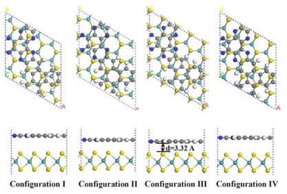
The interlayer interaction between C4N and MoS2 is van der Waals interaction which would affect the structural stability and electronic properties of the fabricated layers. In this case, we considered that C4N stack on the MoS2 in different relative matching positions as different configurations. Four representative configurations for heterostructure are discussed, as shown in Fig. 1.

|
Download:
|
| Fig. 1. Geometric structures of the C4N/MoS2 heterostructures with different configurations. | |
After geometric optimization, the C4N monolayer surface showed a little deformation which is similar with the results observed in g-C3N4/MoS2 nanocomposite [34]. The total energy, equilibrium distance, binding energy and bandgap are calculated and the results are listed in Table 1. By comparing the total energies of these configurations, the configuration Ⅲ with the lowest total energy is the most stable structure of C4N/MoS2 there. The comparison between different configurations is not only in energy but also in the interlayer distance. The equilibrium distances are calculated to be 3.32 Å to 3.46 Å, which are the typical vdW equilibrium spacings. The most stable configuration has the shortest the interlayer space, indicating strong physical interaction between the two independent layers. This phenomenon has also observed in SiC/MoS2 [41], graphene/ZnO [44] and Blue phosphorus/g-GeC heterostructure [16].
|
|
Table 1 Calculation results of the C4N/MoS2 heterostructure. |

To determine the thermodynamic stability of the C4N/MoS2 heterostructure the binding energies (Eb) are calculated from formula: Eb = ET + EC – EM, where ET, EC and EM are the total energies of heterostructures, C4N layer and MoS2 layer. It is clear to find that the binding energy of configuration Ⅲ is -11.94 eV (-86.1 MeV/Å2), which is more negative than that of other configurations. The vdW interaction is stronger than that of C2N/C3N4 (-16.9 MeV/Å2) [45], g-C3N4/MoS2 (-17.8 MeV/Å2) [31] and ZnO/MoS2 (-31.11 MeV/Å2) [17], which indicates its high thermal stability. Overall, the structure of configuration Ⅲ is a fairly qualified vdW heterostructure. Hence, the configuration Ⅲ was selected as the following research model system.
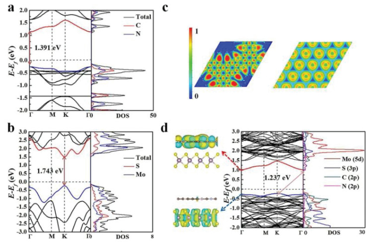
To investigate the enhanced photocatalytic activity of C4N/MoS2 heterostructure, the band structures of the C4N monolayer, MoS2 monolayer and C4N/MoS2 heterostructure are calculated as shown in Fig. 2. The calculated results indicate that the C4N monolayer has a direct band gap of 1.391 eV in which the valence band maximum (VBM) and conduction band minimum (CBM) are located at the Γ point as shown in Fig. 2a. The band gap of MoS2 monolayer (1.743 eV) is a direct band gap at the K point as shown in Fig. 2b which is slightly smaller than the experimental results (1.8 eV) and it is close to previous calculation reports (1.68 eV, 1.97 eV) [43, 26, 41, 46, 47]. The density of states (DOS) of C4N and MoS2 monolayer are also calculated indicating C, N elements have equal contribution to CBM and VBM in C4N monolayer and Mo element has main contribution to CBM and VBM in MoS2 monolayer. Moreover, to investigate the bonding nature in the monolayers, the electron localization function (ELF) is performed as well, as shown in Fig. 2c. From the ELF analysis, ELF = 0.5 presents all around the atoms confirming the presence of π electrons delocalized over the planer C4N monolayer. The ionic character in the MoS2 monolayer's bonds is confirmed by the ELF value of 1 around S atoms and 0.5 observed around Mo atoms.

|
Download:
|
| Fig. 2. Band structures and Density of States (DOS) of (a) C4N and (b)MoS2 monolayer. (c) The electron localization function (ELF) of the C4N and MoS2 monolayer, (d) Band structure, DOS and wave functions of the C4N/MoS2 heterostructure. | |
Compared with the band structure of C4N monolayer and MoS2 monolayer, the band structure of C4N/MoS2 heterostructure is not a simple superimposition of the C4N monolayer and MoS2 monolayer. The band structure is influenced by the vdW interaction between two layers. From the Fig. 2d, C4N/MoS2 heterostructure shows an indirect band gap of 1.237 eV in which the CBM at the Γ point and the VBM at the K point. The electronic structures of other three representational configurations were also calculated and added as shown in Fig. S1 (Supporting information). The band gap is smaller than those of C4N monolayer and MoS2 monolayer which indicates constructing heterostructure can enhance the lower energy absorption. Obviously, the VBM is contributed by the elements of MoS2 monolayer and the CBM is attributed by C4N monolayer. Besides, we also calculated projected density of states (PDOS) with between -2 eV and 3 eV to analyze the electronic structure of C4N/MoS2 heterostructure.
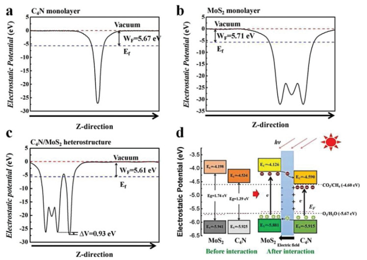
It is clear to find that the VBM is mainly attributed by 5d state of Mo atoms and slightly by C and N atoms. On the other hand, the CBM has equal contributions from 2p states of C and N atoms. The CBM and VBM of the heterostructure reside on different monolayers. This analysis is further demonstrated by the wave functions of the CBM and VBM shown in Fig. 2d. The VBM resides on the MoS2 layer, while its CBM presents entirely on the C4N monolayer. On basis of above analysis, we found that the C4N/MoS2 heterostructure was a typical type-Ⅱ band alignment structure. The work function is a crucial parameter in investigating the charge transfer of the interface and band alignment in composite materials. The work function is defined as WF = EV - EF, where EV is the vacuum level, and EF is the Fermi level [48, 49]. To gain further insights into the C4N/MoS2 heterostructure, the work functions of isolated C4N layer, MoS2 layer and the whole heterostructure were calculated respectively, and shown in Figs. 3a-c. We artificially set the vacuum level to 0, and the Fermi level relative to the vacuum level would equal to the opposite value of the work function after artificial setting. The work function of the C4N is 5.67 eV corresponding to the relative Fermi level is -5.67 eV. The work function of the MoS2 is 5.71 eV which is similar with the value of Li's work (5.68 eV) [41]. And the Fermi level of the MoS2 is -5.71 eV. Besides, the work function of the heterostructure is 5.61 eV corresponding to the Fermi level is -5.61 eV. It can be found that the two monolayers' Fermi levels would reach the similar level after forming the C4N/MoS2 heterostructure.

|
Download:
|
| Fig. 3. Electrostatic potential of the (a) C4N monolayer, (b) the MoS2 monolayer and (c) the C4N/MoS2 heterostructure. (d) The photocatalytic mechanism of the C4N/MoS2 heterostructure and band edge potentials of the C4N, MoS2 monolayer and the C4N/MoS2 heterostructure comparing with reduction potential and oxidation potential of CO2/ CH4 and O2/H2O. | |
According to the theory of solid physics, once two semiconductors with different Fermi energy levels interact with each other on the absence of solar, electrons in the semiconductor with higher Fermi level will transfer to the semiconductor with lower Fermi level, which would result to the appearance of built-in electric field. Electrons would transfer from C4N with higher Fermi level to MoS2 with lower Fermi level in the process of forming C4N/ MoS2 heterostructure. Thus, the negative charges would accumulate in the MoS2 layer and the C4N layer would carry positive charges. The fermi level of the two layers reaches the same value finally. Due to the charge transfer between two layers, unbalanced charge distribution occurs at the interface of the heterostructure. As a result, a built-in electric filed is formed at the interface with the direction from C4N layer to MoS2 layer as shown in Fig. 3d. The potential drop ΔV can evaluate the built-in electric field intensity. The electrostatic potential drop across the C4N/MoS2 interface is 0.93 eV shown in Fig. 3c, which could further confirm the existence of built-in electric field in the heterostructure. And the electric field intensity is related to the electrostatic potential energy difference between two monolayers [50]. The built-in electric field can separate photogenerated electron-hole pairs and prevent the recombination of photogenerated electrons and holes which greatly increase the lifetime of photogenerated electrons and holes. Consequently, under the irradiation of light, the electrons and holes would be generated in C4N and MoS2 layer of the heterostructure. The photogenerated electrons in MoS2 layer would flow into C4N layer and produce reactive sites for reduction reaction like CO2RR. On the other hand, the photogenerated holes would transfer from C4N layer to MoS2 layer producing reactive sites for oxidation reaction like OER. Thus, the C4N/MoS2 heterostructure has enhanced photocatalytic activity of C4N monolayer and MoS2 monolayer.
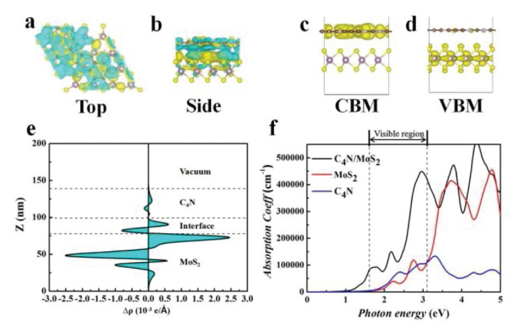
The activity of photocatalytic CO2 reduction reaction to CH4 for the C4N/MoS2 heterostructure is evaluated by comparing the band edge potential relative to the reduction potential and oxidation potential. Thermodynamically, the CBM must be higher than the CO2/CH4 reduction potential (0.16 V vs. NHE at pH 0), while the VBM must be located below the O2/H2O oxidation potential (1.23 V vs. NHE at pH 0). The band edges of the C4N monolayer, the MoS2 monolayer and the C4N/MoS2 heterostructure are calculated with respect to the vacuum level and plotted in the Fig. 3d. It is clear to show that both the band edges of the monolayers and the heterostructure straddle the reduction potential and oxidation potential of CO2/CH4 and O2/H2O and they favor the whole CO2 reduction reaction. The band decomposed charge density for VBM and CBM of heterostructure was also calculated and plotted in Figs. 4a and b. The CBM of the C4N/MoS2 heterostructure is occupied by the electron orbitals of C4N, whereas the VBM is occupied by the electron orbitals of MoS2, which is consistent with the above DOS and wave function analysis. Thus, the CO2 would be reduced on C4N layer till to CH4, and the OER would appear in MoS2 layer. Moreover, the C4N/MoS2 heterostructure has a smaller bandgap comparing to the C4N and MoS2 monolayer, which indicates it can utilize the energy of visible light in a wider wavelength range.

|
Download:
|
| Fig. 4. (a, b) The charge density difference. (c, d) Band decomposed charge density of the C4N/MoS2 heterostructure and (e) planar averaged charge density difference of the C4N/MoS2 heterostructure. (f) The optical spectrum of the C4N, MoS2 monolayer and the C4N/MoS2 heterostructure. | |
The three-dimensional chargedensitydifferencewasalso calculated to further explore the charge transfer and separation between the C4N and MoS2 layer, as shown in the Figs. 4c and d. The charge density difference is defined as Δρ = ρC4N/MoS2 - ρC4N - ρMoS2, while ρC4N/MoS2, ρC4N and ρMoS2 are charge densities of the heterostructure, C4N and MoS2 monolayers. It clearly shows that charge density is redistributed within the C4N/MoS2 interface. The yellow region represents electron accumulation, and the cyan region shows electron depletion. At the interface of the heterostructure, the electrons mainly accumulate in the C4N layer and deplete in the MoS2 surface, which indicates electrons transfer from MoS2 layer to C4N layer through interface. The result is the same as that of previous electric field analysis. Furthermore, the planar averaged charge density difference along the Z direction of the C4N/MoS2 heterostructure was also calculated as shown in Fig. 4e. The positive values indicate the charge accumulation and the negative values indicate the charge depletion. It reveals the charge density rearrangement within two layers and confirms the charge transfer from MoS2 to C4N layer. Thus, the accumulation of electrons in C4N layer and depletion in MoS2 layer would intuitively prove the existence of built-in electric field which produces reaction active sites for CO2RR and OER.
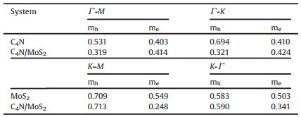
Charge carrier mobility plays an important role in determining the catalytic activity of a photocatalyst. Based on the BardeenShockley approach [51], the smaller effective mass of charge carriers is, the higher charge mobility is. To evaluate the charge carrier mobility of the heterostructure, we calculated the effective charge mass as shown in Table 2. For the heterostructure, the effective mass of holes along the Γ -M and Γ -K direction is smaller than that along the K-M and K-Γ Γ direction. The effective mass of electrons along the Γ -M and Γ -K direction is larger than that along the K-M and K-Γ direction. We find that the effective mass of holes of the C4N/MoS2 heterostructure is overall smaller than that of the C4N monolayer. Similarly, the effective mass of electrons of the C4N/MoS2 heterostructure is smaller than that of MoS2 monolayer. The phenomenon implies the heterostructure possesses higher charge carrier mobility of photogenerated holes and electrons comparing to the C4N monolayer and MoS2 monolayer, respectively. The experiments have demonstrated the direct correlation between charge carrier mobility and photocatalytic activity [52]. Thus, the improvement of charge carrier mobility for the C4N/MoS2 heterostructure indicates that complex of C4N and MoS2 would enhance the photocatalytic activity.
|
|
Table 2 Effective charge mass of C4N, MoS2 and C4N/MoS2 heterostructure. |
The optical absorption is another important parameter to explain the photocatalytic performance of materials and it is directly proportional with photocatalytic activities. Therefore, the optical absorption spectra of the C4N monolayer, MoS2 monolayer and C4N/MoS2 heterostructure are investigated by calculating their imaginary part of the dielectric function, as shown in Fig. 4f. We find that the C4N/MoS2 heterostructure possesses a broad absorption in the visible light range (1.55–3.1 eV) and the absorption coefficient of the C4N/MoS2 heterostructure is much larger comparing to that of the C4N and MoS2 monolayer. Besides, the absorption edge is significantly shifted down by about 0.85 eV. These results indicate that the C4N/MoS2 heterostructure utilized the visible light much more than the individual monolayers. Hence, the C4N/MoS2 heterostructure can utilize the visible light sufficiently and it is an efficient visible light harvesting photocatalyst.
Using first-principles calculations, we systematically study the geometric stability, electronic properties and optical properties of the C4N/MoS2 heterostructure. The C4N/MoS2 is constructed by C4N and MoS2 monolayer and the interaction between the two layers is van der Waals interaction. The negative binding energy and the equilibrium distance of the heterostructure ensure its thermodynamic stability. Comparing with the C4N monolayer and MoS2 monolayer, the C4N/MoS2 heterostructure has a smaller band gap which can utilize more visible light. The band edge potential straddled the redox potential of CO2RR indicates the C4N/MoS2 heterostructure can be a new photocatalyst for CO2 reduction reaction from CO2 to CH4 thermodynamically. Furthermore, the type-Ⅱ band alignment and the difference of work function indicate a built-in electric field is formed within the heterostructure. The built-in electric field could separate the photogenerated electrons and holes efficiently which produce active sites for photocatalytic reaction and enhance photocatalytic activity. More importantly, the optical absorption coefficient of the C4N/MoS2 heterostructure is significantly higher than that of the C4N monolayer and MoS2 monolayer. Therefore, the C4N/MoS2 heterostructure is obviously an efficient photocatalyst, which has strong redox ability. Our results reveal that the C4N/MoS2 heterostructure can be used as an efficient photocatalyst and has potential developments in photocatalytic application.
Declaration of competing interestThe authors declare that they have no known competing financial interests or personal relationship that could have appeared to influence the work reported in this paper.
AcknowledgmentsThis work was supported by Technological Innovation Talents of Harbin Science and Technology Bureau (No. 2017RAQXJ101), the Fundamental Research Foundation for Universities of Heilongjiang Province (No. LGYC2018JC008) and also supported by the Beijing National Laboratory for Molecular Sciences (No. BNLMS201911) and the Young Scholar Training Program of Jilin University.
Appendix A. Supplementary dataSupplementarymaterial related to this article can befound, in the online version, at doi:https://doi.org/10.1016/j.cclet.2020.04.055.
| [1] |
Y. Yan, H. Zhao, Eur. Phys. J. B 86 (2013) 137-139. DOI:10.1140/epjb/e2013-30833-9 |
| [2] |
K.S. Novoselov, A.K. Geim, S.V. Morozov, et al., Science 306 (2004) 666. DOI:10.1126/science.1102896 |
| [3] |
J. Xue, J. Sanchez-Yamagishi, D. Bulmash, et al., Nat. Mater. 10 (2011) 282. DOI:10.1038/nmat2968 |
| [4] |
Z. Guo, S. Furuya, J. Iwata, et al., Phys. Rev. B 87 (2013) 235435. DOI:10.1103/PhysRevB.87.235435 |
| [5] |
Y. Wu, Q. Chen, S. Liu, et al., Chin. Chem. Lett. 30 (2019) 2186-2190. DOI:10.1016/j.cclet.2019.08.014 |
| [6] |
W.J. Ong, L.L. Tan, Y.H. Ng, et al., Chem. Rev. 116 (2016) 7159-7329. DOI:10.1021/acs.chemrev.6b00075 |
| [7] |
X. Zhang, X. Xie, H. Wang, et al., J. Am. Chem. Soc. 135 (2013) 18-21. DOI:10.1021/ja308249k |
| [8] |
Q. Lu, Y. Yu, Q. Ma, et al., Adv. Mater. 28 (2016) 1917-1933. DOI:10.1002/adma.201503270 |
| [9] |
A. Bogucki, Ł. Zinkiewicz, M. Grzeszczyk, et al., Light Sci. Appl. 9 (2020) 48. DOI:10.1038/s41377-020-0284-1 |
| [10] |
Z.Y. Zhu, Y.C. Cheng, U. Schwingenschlogl, Phy. Rev. B 84 (2011) 153402. DOI:10.1103/PhysRevB.84.153402 |
| [11] |
S. Psilodimitrakopoulos, L. Mouchliadis, I. Paradisanos, et al., Light Sci. Appl. 7 (2018) 18005. DOI:10.1038/lsa.2018.5 |
| [12] |
W. Hu, J. Yang, Com. Mater. Sci. 112 (2016) 518-523. DOI:10.1016/j.commatsci.2015.06.033 |
| [13] |
L. Huang, M. Zhong, H. Deng, et al., Sci.China-Phys.Mech.Astron. 3 (2019) 037311. |
| [14] |
J.J. Huang, J.H. Yu, F.Q. Bai, J.Q. Xu, Crystal Grow. Des. 18 (2018) 5353-5364. DOI:10.1021/acs.cgd.8b00773 |
| [15] |
W. Hu, Z. Li, J. Yang, J. Chem. Phys. 139 (2013) 154704. DOI:10.1063/1.4824887 |
| [16] |
X. Gao, Y. Shen, Y. Ma, et al., Appl. Phys. Lett. 114 (2019) 093902. DOI:10.1063/1.5082883 |
| [17] |
S. Wang, C. Ren, H. Tian, et al., Phys. Chem. Chem. Phys. 20 (2018) 13394-13396. DOI:10.1039/C8CP00808F |
| [18] |
J. Bian, J. Feng, Z. Zhang, et al., Angew. Chem. Inter. Ed. 58 (2019) 10873-10878. DOI:10.1002/anie.201905274 |
| [19] |
L. Wang, W. Chen, D. Zhang, et al., Chem. Soc. Rev. 48 (2019) 5310-5315. DOI:10.1039/C9CS00163H |
| [20] |
Y. Yang, M. Wu, X. Zhu, et al., Chin. Chem. Lett. 30 (2019) 2065-2088. DOI:10.1016/j.cclet.2019.11.001 |
| [21] |
C. Yang, Z.D. Yang, H. Dong, et al., ACS Energy Lett. 4 (2019) 2251-2258. DOI:10.1021/acsenergylett.9b01691 |
| [22] |
S. Lin, C.S. Diercks, Y.B. Zhang, et al., Science 349 (2015) 1208. DOI:10.1126/science.aac8343 |
| [23] |
S. Yang, W. Hu, X. Zhang, et al., J. Am. Chem. Soc. 140 (2018) 14614-14618. DOI:10.1021/jacs.8b09705 |
| [24] |
C. Yang, Z.D. Yang, R. Zhang, et al., Chem. Phys. 517 (2019) 104-112. DOI:10.1016/j.chemphys.2018.10.013 |
| [25] |
L. Stegbauer, K. Schwinghammer, B.V. Lotsch, Chem. Sci. 5 (2014) 2789-2790. DOI:10.1039/C4SC00016A |
| [26] |
H.L. Zhuang, R.G. Hennig, J. Phys. Chem. C 117 (2013) 20440-20445. DOI:10.1021/jp405808a |
| [27] |
C. Cheng, J.T. Sun, X.R. Chen, et al., Nanoscale 8 (2016) 17854. DOI:10.1039/C6NR04235J |
| [28] |
Y. Yan, B. Xia, Z. Xu, et al., ACS Catal. 4 (2014) 1693-1705. DOI:10.1021/cs500070x |
| [29] |
J. Kang, S. Tongay, J. Zhou, et al., Appl. Phys. Lett. 102 (2013) 012111. DOI:10.1063/1.4774090 |
| [30] |
T. Guo, L. Wang, S. Sun, et al., Chin. Chem. Lett. 30 (2019) 1253-1260. DOI:10.1016/j.cclet.2019.02.009 |
| [31] |
J. Wang, Z. Guan, J. Huang, et al., J. Mater. Chem. A 2 (2014) 7960. DOI:10.1039/C4TA00275J |
| [32] |
D. R.Kumar.Das, A.K. Singh, J. Cat. 359 (2018) 143-150. DOI:10.1016/j.jcat.2018.01.005 |
| [33] |
G. Kresse, J. Furthmiiller, Comput. Mater. Sci. 6 (1996) 15-50. DOI:10.1016/0927-0256(96)00008-0 |
| [34] |
W. Jian, R. Jia, H.X. Zhang, et al., Inorg. Chem. Front. 7 (2020) 1741-1749. DOI:10.1039/D0QI00102C |
| [35] |
G. Kresse, D. Joubert, Phys. Rev. B Condens. Matter Mater. Phys. 59 (1999) 1758-1775. DOI:10.1103/PhysRevB.59.1758 |
| [36] |
M. Ernzerhof, G.E. Scuseria, J. Chem. Phys. 10 (1999) 5029-5036. |
| [37] |
J.P. Perdew, K. Burke, M. Ernzerhof, Phys. Rev. Lett. 77 (1996) 3865-3868. DOI:10.1103/PhysRevLett.77.3865 |
| [38] |
S. Grimme, J. Antony, S. Ehrlich, H. Krieg, J. Chem. Phys. 132 (2010) 154104. DOI:10.1063/1.3382344 |
| [39] |
S. Grimme, S. Ehrlich, L. Goerigk, J. Comput. Chem. 32 (2011) 1456-1465. DOI:10.1002/jcc.21759 |
| [40] |
S. Saha, T. Sinha, A. Mookerjee, Phys. Rev. B 62 (2000) 8828-8834. DOI:10.1103/PhysRevB.62.8828 |
| [41] |
Q. Li, L. Xu, K.W. Luo, et al., Mater. Chem. Phys. 216 (2018) 64-71. DOI:10.1016/j.matchemphys.2018.05.063 |
| [42] |
Y.C. Rao, S. Yu, X.M. Duan, Phys. Chem. Chem. Phys. 19 (2017) 17252-17254. |
| [43] |
K.F. Mak, C. Lee, J. Hone, et al., Phy. Rev. Lett. 105 (2010) 136805. DOI:10.1103/PhysRevLett.105.136805 |
| [44] |
W. Geng, X. Zhao, H. Liu, X. Yao, J. Phys. Chem. C 117 (2013) 10536. DOI:10.1021/jp401733h |
| [45] |
H. Wang, X. Li, J. Yang, Chem. Phys. Chem. 17 (2016) 2100-2104. DOI:10.1002/cphc.201600209 |
| [46] |
J. Liao, B. Sa, J. Zhou, et al., J. Phys. Chem. C 118 (2014) 17594-17599. DOI:10.1021/jp5038014 |
| [47] |
N. Singh, G. Jabbour, U. Schwingenschlogl, Eur. Phys. J. B 85 (2012) 392-398. DOI:10.1140/epjb/e2012-30449-7 |
| [48] |
J. Liu, B. Cheng, J. Yu, Phys. Chem. Chem. Phys. 18 (2016) 31177. |
| [49] |
S. Wei, F. Wang, P. Yan, et al., J. Catal. 377 (2019) 122-132. DOI:10.1016/j.jcat.2019.07.024 |
| [50] |
X. Li, Z. Li, J. Yang, Phys. Rev. Lett. 112 (2014) 018301. DOI:10.1103/PhysRevLett.112.018301 |
| [51] |
J. Qiao, X. Kong, Z.X. Hu, et al., Nat. Commun. 5 (2014) 4475. DOI:10.1038/ncomms5475 |
| [52] |
P.A. DeSario, J.J. Pietron, D.H. Taffa, et al., J.Phys.Chem.C 119 (2015) 17529-17538. DOI:10.1021/acs.jpcc.5b04013 |