 2020, Vol. 31


b Ames Laboratory, US DOE, Ames, IA 50011, United States
Supercapacitors (SCs) have attracted considerable attention because they possess fast dynamic response, excellent charge-discharge efficiency and superior cycling stability. In addition, SCs can also provide instantaneously a higher power density than batteries and higher energy density than conventional dielectric capacitors [1, 2]. Therefore, SCs were widely used in portable electronics, power back-up, electrical vehicles and other electronic devices for the purpose of power enhancement. In recent years, the studies of energy storage devices were concentrated on all-solidstate (ASS) asymmetric SCs, because they are safer with no risk of the leakage of electrolyte [3, 4]. Moreover, the asymmetric design can widen the operation voltage window and further improve the energy density of the devices.
Electrode active materials are key component to fabricate high performances SCs. Generally, the active materials can be divided into two types based on different electron storage mechanisms: One family, traditional electrical double layered capacitors (EDLCs), such as active carbon (AC) [5], carbon nanotubes (CNT) [6, 7], graphene or doped graphene [8, 9], which store energy by accumulation of charges in the electrical double layer near the electrode/electrolyte interface. They are very stable during the charge/discharge (CD) process but suffer relatively low specific capacitance. The other family is electrochemical capacitor, which store energy via Faradaic redox reaction at electrode surface, such as NiO [10], Co3O4 [11, 12], MnO2 [13-15], NiCo2O4 [16-18], NiCoS [19-23] and metal-organic frameworks (MOFs) [24, 25], these electroactive materials possess high theoretical capacitance, whereas they lack of mechanical properties and electrical conductivity.
Metal selenides have received considerable attention due to its enormous applications in the fields of optics, photocatalysis and sensor [26-29]. Compared with the metal oxides, transition metal selenides exhibit much enhanced electrical conductivity due to the anion exchange providing smaller bandgap [30]. In addition, the substitution of oxygen with selenium could create more flexible structure because the electronegativity of selenide is lower than that of oxide. Some metal selenides, such as hierarchical GeSe nanostructures [31], MoSe2 nanosheets [32], CoSe nanosheets [33], SnSe and SnSe2 nanosheets [34, 35], CuSe nanosheet arrays [36] have been extensively studied and displayed superior electrochemical properties when using as electrode active materials. Among these metal selenides, nickel selenide is regarded as a valuable material for supercapacitance and lithium battery [37, 38], which is also considered as a less toxic and more environmentally responsible alternative. Although the synthesis and characterization of nickel selenide nanostructures have been reported, preparation of nickel selenide thin films by electrochemical deposition and their application in SC is rarely explored.
In this paper, nickel selenide thin films with different phases were successfully fabricated on stainless-steel sheet using a facile, effective electrodeposition technique. Morphologies, microstructures and chemical compositions of the nanosheet films were characterized systematically. Electrochemical tests exhibit that their maximum mass specific capacitance of Ni3Se2 and NiSe could reach 581.1 F/g at the current density of 1 A/g and 1644.7 F/g at the current density of 2 A/g, respectively. These values are much higher than those of carbonous materials, and comparable to most of reported transition metal oxides. The capacitance retention of Ni3Se2 and NiSe thin films keeps 90.1% and 75.0% of its initial value respectively after 10, 000 cycles. Due to their high specific capacitance and superior electrochemical stability, a flexible ASS asymmetric SCs were assembled by utilizing NiSe films as positive electrode and activated carbon as negative electrode. The solid device delivers a high areal capacitance of 27.0 mF/cm2 at the current density of 0.7 mA/cm2 with robust cycling stability (~84.6% capacitance retention after 10, 000 cycles. The maximum volumetric energy density and power density of the NiSe//AC asymmetric SCs can achieve 0.26 mWh/cm3 and 33.35 mW/cm3, respectively. These values are much higher than those of reported symmetric and asymmetric SCs. Moreover, two solid devices in series can light up a red light-emitting diode displaying great potential for energy storage.
Nickel selenide thin films were deposited in a standard three-electrode configuration using a stainless-steel sheet, a Pt sheet, and a saturated calomel electrode (SCE) as the working electrode, counter electrode, and reference electrode, respectively. In order to explore the effect of electrolyte concentration on the morphology and performance of nickel selenide thin films, the concentrations of SeO2 were adjusted from 10 mmol/L to 100 mmol/L while keeping Ni(CH3COO)2 concentrations at 10 mmol/L. 0.1 mol/L KCl were used to enhance the conductivity of the solution. The pH value was adjusted to 3.5 with 0.2 mol/L hydrochloric acid.
For the preparation of flexible asymmetric SC devices, NiSe/ stainless-steel and AC/stainless-steel were used as positive electrode and negative electrode respectively. PVA-KOH gel was used as electrolyte and cellulose septum was used as separator. NiSe/stainless-steel and AC/stainless-steel were immersed in the PVA-KOH gel solution for 2 min in order to adsorb a layer of the solid electrolyte. After the evaporation of the excessive water, the septum was adhered in the middle of two electrodes and the device with a sandwich structure was assembled. Finally, the device was dried in a vacuum oven at 50 ℃ for 12 h. The AC thin films were fabricated as previous work. AC (YP-50 F, Kurary) (80%), conductive carbon black (10%) and polytetrafluoroethylene (PTFE) (10%) were added in N-methy pyrrolidone (C5H9NO) under vigorous stirring [39]. The preparation of PVA-KOH gel electrolyte was performed as follows: 3 g KOH was added to the 10 mL deionized water. 6 g PVA was added into 50 mL of deionized water and stirred at 85 ℃ until the solution became limpid, then the solution was cooled to room temperature. After that, the KOH solution was dropped into PVA solution to form gel electrolyte [40, 41].
Cyclic voltammetry (CV), galvanostatic charge/discharge (GCD) and electrochemical impedance spectroscopy (EIS) were examined systematically with an electrochemical workstation (CHI 660E, Chenhua Co., Shanghai). The electrochemical performances of nickel selenide thin films were performed in a three-electrode system in 1.0 mol/L aqueous KOH electrolyte.
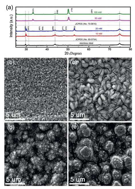
The deposited films were first characterized using XRD. Fig. 1a shows the typical XRD patterns of nickel selenide thin films deposited at different electrolyte concentration. Data of the stainless-steel substrate were also added for comparison. It is obvious that some diffraction peaks appeared after the electrodeposition. When the SeO2 concentration was kept at 10 mmol/L and 20 mmol/L, the diffraction patterns of the deposited films are almost consistent, which matched well with the JCPDS No. 85-0754 of rhombohedral-type Ni3Se2. When increasing the SeO2 concentration to 50 or 100 mmol/L, the diffraction peaks changed completely, peaks at 32.85°, 33.90°, 44.52°, 61.20°, matched well with hexagonal-type NiSe (JCPDS card No.75-0610). These results indicate that we can control the phase of the nickel selenide with simply changing the SeO2 concentration.

|
Download:
|
| Fig. 1. (a) XRD patterns and SEM images of the nickel selenide thin films deposited at different electrolyte concentration: (b) 10 mmol/L, (c) 20 mmol/L, (d) 50 mmol/L, (e) 100 mmol/L. | |
SEM was used to study the morphology evolution of nickel selenide thin films deposited under different electrolyte concentration. Fig. 1b shows SEM image of the nickel selenide thin films deposited at 10 mmol/L. Apparently, the film is consisting of a large number of compact and uniform nanoparticles. When the electrolyte concentration increased to 20 mmol/L, the nanoparticles turned to bunches of fluffy regular layered structure (Fig. 1c). With increasing the electrolyte concentration to 50 mmol/L, the sizes of these nanoparticles became larger and covered with some tiny vertically-aligned nanorods. These outstretched nanorods could maintain a stable structure when used as an electrode for ASS device (Fig. 1d). The gaps between the nanorods are very beneficial to the diffusion of electrolyte ions, and enable fast redox reaction. It is expected that nickel selenide synthesized under such condition would exhibit enhanced specific capacitance. As the electrolyte concentration continues to increase to 100 mmol/L (Fig. 1e), there are some cracks on the surface of the nickel selenide thin films, which makes the active material easily detached from the substrate. By integrating the above experiments, the nickel selenide thin films deposited at 20 or 50 mmol/L were used as active electrodes to evaluate their chemical properties.
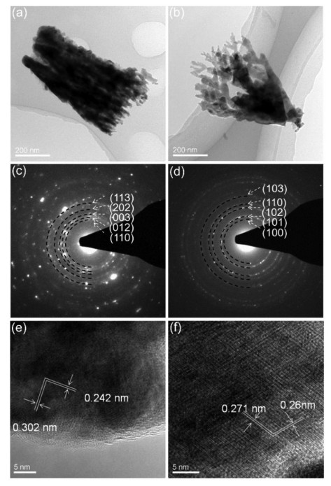
The microstructures of the nickel selenide thin films were further investigated by TEM and high resolution TEM. Figs. 2a and b show the typical TEM images of Ni3Se2 and NiSe nanostructures respectively. The morphology of Ni3Se2 clearly shows significant difference with that of NiSe. Ni3Se2 shows compact structure while NiSe shows dendritic structure. As we know, to construct high-performance electrode materials, it is essential to form interconnected structure for ion diffusion at the interface between the electrolyte and active materials. Here, NiSe was expected to show better electrochemical performance duo to the hierarchical microstructure. Figs. 2c and d show the corresponding selected area electron diffraction (SAED) of Ni3Se2 and NiSe nanostructures, both of them show well-defined diffraction rings, indicating their polycrystalline nature. The measured d-spacings in Fig. 2c are 0.310, 0.295, 0.242, 0.212 and 0.189 nm, which are close to the interplanar of (110), (012), (003), (202) and (113) planes of Ni3Se2 (JCPDS No. 85-0754). The measured d-spacings in Fig. 2d are 0.321, 0.275, 0.206, 0.185 and 0.156 nm, which are close to the interplanar of (100), (101), (102), (110) and (103) planes of NiSe (JCPDS No. 75-0610). High-resolution TEM were also conducted to study their microstructure as shown in Figs. 2e and f. The clearly lattice fringe of Ni3Se2 and NiSe indicated their high crystallinity. The measured lattice spacings are 0.302 and 0.242 nm, which are correspond to (110) and (003) interplanar separation of Ni3Se2 (JCPDS No. 85-0754). And the measured lattice spacing of NiSe nanosheets are 0.271 and 0.26 nm, which are identified with (101) and (002) interplanar separation (JCPDS No. 75-0610). Based on the above results, it is concluded that the as-obtained products are Ni3Se2 and NiSe, respectively.

|
Download:
|
| Fig. 2. (a, b) TEM images, (c, d) SAED patterns, (e, f) corresponding high resolution TEM images of the as-prepared nickel selenide thin films. | |
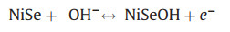
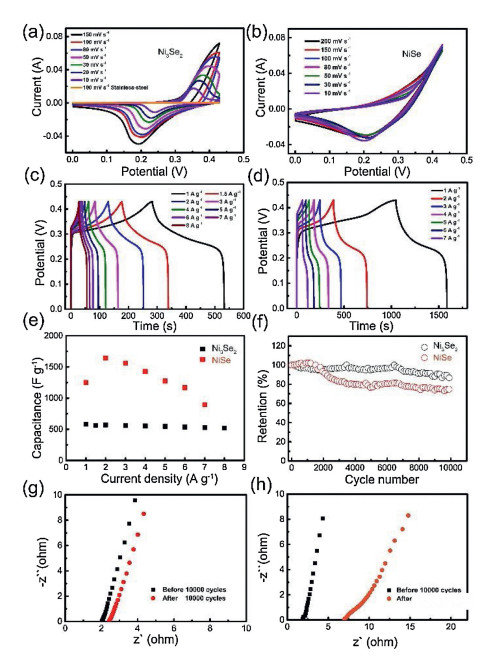
The electrochemical performance of Ni3Se2 and NiSe thin films were tested in a classical three-electrode system using 1 mol/L KOH as the electrolyte. The mass of the active materials were about 1.0 mg and 5.0 mg, respectively. Fig. 3a shows the CV curves of Ni3Se2 thin films in a potential window of 0–0.43 V (vs. SCE). A pair of redox peaks were observed demonstrating a Faradaic-capacity behavior during energy storage process. With increasing the scanning rate from 10 mV/s to 100 mV/s, the specific currents increased and the redox peaks shifted, indicative of the quasireversible nature of the redox reactions. Pure stainless-steel substrate was tested in the same voltage window with a scan rate of 100 mV/s, the integrated CV area of the stainless-steel substrate is much lower than that of Ni3Se2 and NiSe thin films, which implies that the effect of the substrate on the overall capacitance can be ignored. Fig. 3b shows the CV curves of NiSe thin films. The shapes show a little difference compared with that of Ni3Se2. However, the shapes of the curves nearly unaltered, which indicate that the electrode possesses superior electrochemical performance. The suggested redox mechanism of NiSe in aqueous alkaline solution can be expressed as reaction 1 [42]:
|
(1) |

|
Download:
|
| Fig. 3. CV curves of (a) Ni3Se2 and (b) NiSe. GCD curves of (c) Ni3Se2 and (d) NiSe. (e) The calculated specific capacitance of Ni3Se2 and NiSe. (f) Cycling stability measured at a current density of 10 A/g. Nyquist plots of (g) Ni3Se2 and (h) NiSe before and after 10, 000 cycles. | |
Figs. 3c and d illustrate the GCD curves of Ni3Se2 and NiSe thin films at different current densities from 1.0 A/g to 7.0 A/g respectively, the charge and discharge curves are almost symmetrical, which confirmed the modified capacitive nature and superior electrochemical reversibility, matching well with the redox peaks in the CV curves. Fig. 3e displays the calculated specific capacitance of Ni3Se2 and NiSe thin films at different current densities. For the Ni3Se2 thin films, the maximum mass specific capacitance could attain 581.1 F/g at the current density of 1 A/g. However, the maximum mass specific capacitance of NiSe is 1644.7 F/g at the current density of 2 A/g, which approximately tripled that of Ni3Se2. Such a large mass specific capacitance is much higher than those of carbonous materials [3, 5, 6, 8, 43-46] and comparable to those of transition metal oxides/sulfides [10, 13, 16, 28, 31, 40, 47-49]. The cycling stability were performed by continuous charge/discharge measurements at the current density of 10 A/g as shown in Fig. 3f, the capacitance retention after 10, 000 cycles of Ni3Se2 and NiSe thin films reaches 90.1% and 75.0% of its initial value, respectively. This indicates that the electrode possesses great electrochemical stability. Figs. 3g and h show the EIS spectrums of the Ni3Se2 and NiSe thin films electrodes before and after 10000 cycles respectively. At the initial stage, both of them displayed the similar slope at the low frequency region, indicating their excellent capacitive behaviors. At high frequency region, they exhibited comparable equivalent series resistance (ESR) of ~2.0 Ω, assigning to the similar resistance of ionic diffusion. However, after 10000 CD processes, the ESR of NiSe increased subtlety from 2.05 ohm to 7.11 ohm, which indicate that some nonreversible changes may accrue in the long-time cyclic process.
On the basis of the superior electrochemical property of NiSe thin film electrodes, a flexible ASS asymmetric SCs were assembled by utilizing NiSe films as positive electrode and activated carbon as negative electrode. The electrochemical performances of AC were shown in Fig. S1 (Supporting information). Since the voltage window of NiSe thin films were tested at a steady voltage window of 0 to 0.43 V, while that of the AC electrodes were measured from -1.0 V to 0 V, it was expected that the operating cell potential can be extended to 1.43 V by taking advantage of the maximum applied voltage when they are assembled into ASS asymmetric SCs (Fig. 4a). The effective working area of the device is about 3.0 cm2 and the thickness of the device is 0.12 mm (Fig. S2 in Supporting information). To optimized the electrochemical performance of the NiSe//AC asymmetric SCs, mass of NiSe and AC were balanced according to Eqs. S1 and S2 (Supporting information). The CV curves of the ASS-SCs device shown in Fig. 4b were scanned from 10 mV/s to 150 mV/s. It is obvious that the CV plots have distinct redox peaks, indicating the enhanced electrochemical performance and the ability to conduct ions and electrons at high rates. When the operating potential exceeds 0.75 V, the operating current increased immensely, which corresponds to the redox characteristics of the cell originated from the positive electrode. The GCD tests of the ASS asymmetric SCs were performed at various current densities and the related discharging branch curves are shown in Fig. 4c. Accordingly, the corresponding specific areal capacitance were shown in Fig. 4d. The maximum areal capacitance of the NiSe//AC asymmetric SCs reached 27.0 mF/cm2 at the current density of 0.7 mA/cm2, which is much higher than those of previously reported symmetric and asymmetric SCs. Cycle stability of the NiSe//AC asymmetric SCs were also performed using GCD tests at the current density of 10 m-2. As shown in Fig. 4e, the capacitance retention of NiSe//AC asymmetric SCs achieved 84.6% of its initial value after 10, 000 cycles, indicating excellent cycling performance. Fig. 4f shows the Ragone plot of the as-fabricated device as well as some recently reported SCs and other traditional energy storage device. The maximum volumetric energy density and power density of the NiSe//AC asymmetric SCs can achieve 0.26 mWh/cm3 and 33.35 mW/cm3, respectively. Those values are much higher than those of ZnO/MnO2 core/shell nanorod SSCs [47], Cu(OH)2 nanobelts SSCs [48], Bi2O(OH)2SO4 MSCs [50], CNT SSCs [51], Ni-Co selenide nanorod array [52], CoSe nanosheets [53], activated-carbon SSCs [45], TiN nanowire SSCs [54], all carbon SSC [43] and MnO2 tube-in-tube SSCs [49]. Additionally, as a prototype for practical applications, a tandem of two such solid devices can light up a red light-emitting diode (LED, 1.65 V, 2 mA) for approximately 70 s after charging at 2.0 mA/cm2 for 40 s.

|
Download:
|
| Fig. 4. (a) CV curves of NiSe thin film and AC at 100 mV/s. (b) CV curves of the ASS NiSe//AC asymmetric SCs device. (c) GCD curves at various current densities. (d) Calculated specific areal capacitance. (e) Cycle stability of the device at a current density of 0.7 mA/cm2. (f) Ragone plots of ASS NiSe//AC asymmetric SCs device. (g) A red LED lighted by the tandem of two NiSe//AC asymmetric SCs. | |
In many cases, SCs are used as power resource for portable or wearable electronics devices, it is important that the SCs have good mechanical flexibility without losing its electrochemical performance. Fig. S2 shows photos of the ASS-SC at different bending angles or twisted state. The mechanical force does not destroy the physical structure of the ASS-SC, indicative of its superior mechanical flexibility. The electrochemical performances were also checked at the same states as show in Fig. S3 (Supporting information). The CV curves of device show similar capacitive behavior with no obvious capacitance decay at different deformation state.
In summary, nickel selenide thin films with different phases (Ni3Se2, NiSe) were successfully fabricated on stainless-steel sheet using a facile, effective electrodeposition technique. Both of them exhibited high specific capacitance and superior capacitance retention. ASS asymmetric SCs were assembled by utilizing NiSe thin films as positive electrode and activated carbon as negative electrode. The assembled solid device delivered a high areal capacitance specific capacitance of 27.0 mF/cm2 at the current density of 0.7 mA/cm2. The maximum volumetric energy density and power density of the NiSe//AC asymmetric SCs can achieved 0.26 mWh/cm3 and 33.35 mW/cm3, respectively. The device shown robust cycling stability (~84.6% capacitance retention after 10, 000 cycles, outstanding flexibility and satisfactory mechanical stability. Our results demonstrate that NiSe could be great potential active materials for high performance SCs.
Declaration of competing interestThe authors declare no competing financial interest.
AcknowledgmentsThis work was supported by the Fundamental Research Funds for the Central Universities (Nos. 2018B19714 and 2019B02614) and Natural Science Foundation of China (No. 51775253). Work at the Ames Laboratory was supported by the Department of Energy, Division of Materials Sciences & Engineering (No. DE-AC02-07CH11358).
Appendix A. Supplementary dataSupplementary material related tothis article canbefound, in the online version, at doi:https://doi.org/10.1016/j.cclet.2020.03.010.
| [1] |
G. Wang, L. Zhang, J. Zhang, Chem. Soc. Rev. 41 (2012) 797-828. DOI:10.1039/C1CS15060J |
| [2] |
P. Simon, Y. Gogotsi, B. Dunn, Science 343 (2014) 1210-1211. DOI:10.1126/science.1249625 |
| [3] |
T. Lv, M. Liu, D. Zhu, et al., Adv. Mater. 30 (2018) 1705489. DOI:10.1002/adma.201705489 |
| [4] |
H. Pang, X. Li, Q. Zhao, et al., Nano Energy 35 (2017) 138-145. DOI:10.1016/j.nanoen.2017.02.044 |
| [5] |
Y. Huang, L. Peng, Y. Liu, et al., ACS Appl. Mater. Interfaces 8 (2016) 15205-15215. DOI:10.1021/acsami.6b02214 |
| [6] |
W. Jiang, D. Yu, Q. Zhang, et al., Adv. Funct. Mater. 25 (2015) 1063-1073. DOI:10.1002/adfm.201403354 |
| [7] |
Q. Zhang, X. Wang, Z. Pan, et al., Nano Lett. 17 (2017) 2719-2726. DOI:10.1021/acs.nanolett.7b00854 |
| [8] |
L. Feng, K. Wang, X. Zhang, et al., Adv. Funct. Mater. 28 (2018) 1704463. DOI:10.1002/adfm.201704463 |
| [9] |
L. Chen, L. Chen, Q. Ai, et al., Chem. Eng. J. 334 (2018) 184-190. DOI:10.1016/j.cej.2017.10.038 |
| [10] |
J.A. Syed, J. Ma, B. Zhu, et al., Adv. Energy Mater. 7 (2017) 1701228. DOI:10.1002/aenm.201701228 |
| [11] |
C. Zhang, J. Wei, L. Chen, et al., Nanoscale 9 (2017) 15423-15433. DOI:10.1039/C7NR05059C |
| [12] |
M. Zhang, H. Fan, N. Zhao, et al., Chem. Eng. J. 347 (2018) 291-300. DOI:10.1016/j.cej.2018.04.113 |
| [13] |
Z. Yang, J. Gong, C. Tang, et al., J. Mater. Sci.-Mater. Eletron. 28 (2017) 17533-17540. DOI:10.1007/s10854-017-7689-5 |
| [14] |
X. Jia, X. Wu, B. Liu, Dalton Trans. 47 (2018) 15506-15511. DOI:10.1039/C8DT03298J |
| [15] |
H. Liu, D. Zhao, P. Hu, et al., Chin. Chem. Lett. 29 (2018) 1799-1803. DOI:10.1016/j.cclet.2018.11.019 |
| [16] |
C. Zhang, Y. Huang, S. Tang, et al., ACS Energy Lett. 2 (2017) 759-768. DOI:10.1021/acsenergylett.7b00078 |
| [17] |
H.M. Lee, C. Gopi, P. Rana, et al., New J. Chem. 42 (2018) 17190-17194. DOI:10.1039/C8NJ03764G |
| [18] |
H. Liu, D. Zhao, Y. Liu, et al., Chem. Eng. J. 373 (2019) 485-492. DOI:10.1016/j.cej.2019.05.066 |
| [19] |
K. Tao, X. Han, Q. Ma, et al., Dalton Trans. 47 (2018) 3496-3502. DOI:10.1039/C7DT04942K |
| [20] |
X. Han, K. Tao, D. Wang, et al., Nanoscale 10 (2018) 2735-2741. DOI:10.1039/C7NR07931A |
| [21] |
D. Zhao, H. Liu, X. Wu, et al., Nano Energy 57 (2019) 363-370. DOI:10.1016/j.nanoen.2018.12.066 |
| [22] |
K.D. Ikkurthi, S. Rao, J.W. Ahn, et al., Dalton Trans. 48 (2019) 578-586. DOI:10.1039/C8DT04139C |
| [23] |
Y. Liu, D. Zhao, H. Liu, et al., Chin. Chem. Lett. 30 (2019) 1105-1110. DOI:10.1016/j.cclet.2018.12.024 |
| [24] |
L. Jin, X. Li, C. Liu, H. Pang, Chin. Chem. Lett. 31 (2020) 2207-2210. DOI:10.1016/j.cclet.2019.08.044 |
| [25] |
G. Yuan, S. Yu, J. Jie, et al., Chin. Chem. Lett. 31 (2020) 1941-1945. DOI:10.1016/j.cclet.2019.12.034 |
| [26] |
P. Houizot, F. Smektala, V. Couderc, et al., Opt. Mater. 29 (2007) 651-656. DOI:10.1016/j.optmat.2005.11.022 |
| [27] |
X. Wang, Z. Miao, Y. Ma, et al., Nanoscale 9 (2017) 14512-14519. DOI:10.1039/C7NR04851C |
| [28] |
S. Ghosh, P.D. Patil, M. Wasala, et al., 2D Mater. 5 (2018) 015001. |
| [29] |
H. Shuai, X. Wu, K. Huang, et al., Biosens. Bioelectron. 94 (2017) 616-625. DOI:10.1016/j.bios.2017.03.058 |
| [30] |
J. Zhu, S. Tang, J. Wu, et al., Adv. Energy Mater. 7 (2017) 1601234. DOI:10.1002/aenm.201601234 |
| [31] |
X. Wang, B. Liu, Q. Wang, et al., Adv. Mater. 25 (2013) 1369. DOI:10.1002/adma.201370061 |
| [32] |
S.K. Balasingam, J.S. Lee, Y. Jun, Dalton Trans. 44 (2015) 15491-15498. DOI:10.1039/C5DT01985K |
| [33] |
L. Wu, L. Shen, T. Wang, et al., J. Alloy. Comp. 766 (2018) 527-535. DOI:10.1016/j.jallcom.2018.06.353 |
| [34] |
C. Zhang, H. Yin, M. Han, et al., ACS Nano 8 (2014) 3761-3770. DOI:10.1021/nn5004315 |
| [35] |
J. Li, J. Gong, Z. Yang, et al., J. Phys. Chem. C 123 (2019) 29133-29143. DOI:10.1021/acs.jpcc.9b08889 |
| [36] |
L. Li, J. Gong, C. Liu, et al., ACS Omega 2 (2017) 1089-1096. DOI:10.1021/acsomega.6b00535 |
| [37] |
G. Nagaraju, S. Cha, S. Sekhar, et al., Adv. Energy Mater. 7 (2017) 1601362. DOI:10.1002/aenm.201601362 |
| [38] |
S. Wang, S. Ma, Dalton Trans. 48 (2019) 3906-3913. DOI:10.1039/C9DT00041K |
| [39] |
N. Jäckel, D. Weingarth, A. Schreiber, et al., Electrochim. Acta 191 (2016) 284-298. DOI:10.1016/j.electacta.2016.01.065 |
| [40] |
J. Gong, J. Li, J. Yang, et al., ACS Appl. Mater. Interfaces 10 (2018) 38341-38349. DOI:10.1021/acsami.8b12543 |
| [41] |
J. Gong, Y. Tian, Z. Yang, et al., J. Phys. Chem. C 122 (2018) 2002-2011. DOI:10.1021/acs.jpcc.7b11125 |
| [42] |
B. Kirubasankar, V. Murugadoss, J. Lin, et al., Nanoscale 10 (2018) 20414-20425. DOI:10.1039/C8NR06345A |
| [43] |
V.T. Le, H. Kim, A. Ghosh, et al., ACS Nano 7 (2013) 5940-5947. DOI:10.1021/nn4016345 |
| [44] |
Z. Pan, M. Liu, J. Yang, et al., Adv. Funct. Mater. 27 (2017) 1701122. DOI:10.1002/adfm.201701122 |
| [45] |
G. Wang, H. Wang, X. Lu, et al., Adv. Mater. 26 (2014) 2676-2682. DOI:10.1002/adma.201304756 |
| [46] |
J. Zhao, Y. Jiang, H. Fan, et al., Adv. Mater. 29 (2017) 1604569. DOI:10.1002/adma.201604569 |
| [47] |
P. Yang, X. Xiao, Y. Li, et al., ACS Nano 7 (2013) 2617-2626. DOI:10.1021/nn306044d |
| [48] |
S. Lei, Y. Liu, L. Fei, et al., J. Mater. Chem. A 4 (2016) 14781-14788. DOI:10.1039/C6TA06634H |
| [49] |
X.F. Lu, A.L. Wang, H. Xu, et al., J. Mater. Chem. A 3 (2015) 16560-16566. DOI:10.1039/C5TA04526F |
| [50] |
Z. Liu, F. Teng, C. Chang, et al., Nano Energy 27 (2016) 58-67. DOI:10.1016/j.nanoen.2016.06.025 |
| [51] |
Y.J. Kang, H. Chung, C.H. Han, et al., Nanotechnology 23 (2012) 065401. DOI:10.1088/0957-4484/23/6/065401 |
| [52] |
P. Sun, R. Lin, Z. Wang, et al., Nano Energy 31 (2017) 432-440. DOI:10.1016/j.nanoen.2016.11.052 |
| [53] |
X. Zhang, J. Gong, K. Zhang, et al., J. Alloys. Compd. 772 (2019) 25-32. DOI:10.1016/j.jallcom.2018.09.023 |
| [54] |
P. Sun, R. Lin, Z. Wang, et al., Nano Energy 31 (2017) 432-440. DOI:10.1016/j.nanoen.2016.11.052 |