 2020, Vol. 31


b Hunan Institute of Advanced Sensing and Information Technology, Xiangtan University, Xiangtan 411105, China;
c School of Mechanical Engineering, Xiangtan University, Xiangtan 411105, China
Recently, molybdenum disulfide (MoS2) shows great prospects in the field of gas detection at room temperature because of its excellent physical and chemical properties, such as unique layered structure, large surface-to-volume ratio and abundant surface active sites. [1], which makes it a promising candidate for the detection of various hazardous gases, such as NO, NO2 and NH3 [2-5]. However, pure MoS2 is inevitably oxidized as the accumulation of oxygen, which results that MoS2 gas sensors still suffer from weak performance, such as poor long-term stability and incomplete recovery behaviors [6]. In our previous work [7], it had been demonstrated that the modification with PbS can effectively improve the stability and recovery behaviors of MoS2. Due to the competitive adsorption between PbS and MoS2, O2 or NO2 molecules tend to adsorb on the surface of PbS instead of MoS2, which prevents MoS2 from being oxidized and thus improves the stability of MoS2. However, unlike defect-free MoS2 in the theoretical calculation, MoS2 prepared by hydrothermal method is easy to form lots of defects [8-10], so that a certain amount of NO2 is still adsorbed on the surface of MoS2 in the form of chemisorption. In addition, while MoS2 prepared by hydrothermal method is chosen as the modified object, due to its large size and fluffy ball-like structure, majority of the PbS particle are more inclined to deposit on the edge of the fluffy ball-like MoS2, which means that the hydrothermally synthesized MoS2 cannot be adequately modified by PbS. It thus exhibits a relatively low-level improvement in gas-sensing performance. Therefore, as the object of modification, the defect density and morphology of MoS2 are the key factors in determining the effect of improvement after being modified by PbS.
MoS2 nanosheet prepared by mechanical exfoliation is of well-crystallized, few defects and high carrier mobility [11, 12], which is difficult to be achieved by hydrothermal method, chemical vapor deposition (CVD) and other methods. Moreover, due to the flake-like structure of mechanically exfoliated MoS2, PbS can uniformly distribute on the whole surface of MoS2 nanosheet, which means MoS2 can be adequately and effectively modified by PbS. Consequently, MoS2 prepared by mechanical exfoliation is chosen to be the object of modification, which is expected to achieve excellent sensing performance.
In this work, PbS@MoS2 composites are constructed by mechanical exfoliation combining with wet-chemical precipitation, and the plane gas sensor based on PbS@MoS2 is fabricated to investigate its NO2 sensing performance without heating condition. The results indicate that flake-like MoS2 with few defects is confirmed to be of fast response speed and large response value to NO2 after PbS modification. Especially, the response time is reduced by two orders of magnitude, from hundreds of seconds to less than ten seconds. The underlying enhanced gas-sensing mechanism of the PbS@MoS2 based sensor has been further discussed. The modification of PbS for mechanically exfoliated MoS2 provides opportunities for the significantly improved performances of gas sensor.
MoS2 nanosheets prepared by mechanical exfoliation were transferred to the PET substrate with ITO interdigital electrodes, and the detailed processes of MoS2 gas sensor was referred to the previous work [13]. The PbS particles were synthesized using a simple wet-chemical route as follows: 0.331 g Pb(NO3)2 and 0.24 g Na2S·9H2O were dissolved into 40 mL of DI water, and then the mixed solution was ultrasonicated for 1 h. The suspension was separated by centrifugation to remove the upper layer of liquid, and the remaining precipitate was washed repeatedly with DI water and ethanol to remove the unreacted solution. The black powder was obtained after removing the residual solvents by drying at 60 ℃ for 1 h. Subsequently, the as-prepared powder (0.02 g) was uniformly dispersed in ethanol (4 mL) to form a homogeneous suspension, and then 1 μL of suspension was selectively dropped on the surface of the as-prepared MoS2 gas sensor. Finally, PbS@MoS2 gas sensor was directly obtained after drying in vacuum drying oven at 60 ℃ for 1 h. At the same time, the pure MoS2 gas sensor without PbS modification and the pure PbS gas sensor were also prepared for the comparison of gas sensing performance.
The components of as-prepared samples (i.e., MoS2 nanosheets, PbS particles and PbS@MoS2 composites) were measured by Raman spectra with a 532 nm laser excitation (Renishaw, inVia, UK). Field emission scanning electron microscope (FE-SEM, Hitachi SU5000, Japan) with energy-dispersive spectroscope (Bruker QUANTAX-400) was used to observe the morphologies and elements distribution of MoS2 and PbS@MoS2, and the thickness of MoS2 sheets was confirmed by surface profilometer (Ambios Technology, XP-100, U.S.A.). X-ray photoelectron spectroscopy (XPS, Thermo Scientific, ES-CALAB 250Xi, U.S.A.) was performed to analyze the surface composition and chemical states of MoS2 and PbS@MoS2. The gas sensing properties of gas sensors were respectively investigated by a CGS-8 intelligent gas sensing analysis system (Beijing Elite Tech Co., Ltd., China), and all the measurement were operated at room temperature (25 ℃). In this work, the response value was defined as S = Ra/Rg (when Ra > Rg) or S = Rg/Ra (when Ra < Rg) [14, 15], where Rg and Ra are the resistances of gas sensors in target gas atmosphere and air atmosphere, respectively. The response and recovery times of gas sensors were defined as the time required to reach 90% of the total resistance change.
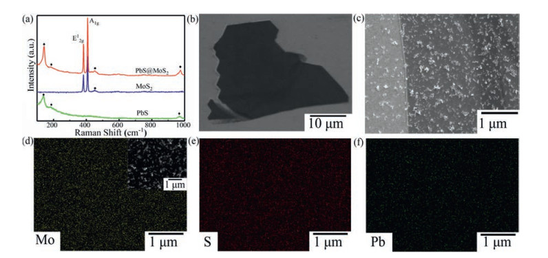
Raman spectroscopy is a convenient and effective technique for qualitative analysis of material components. As depicted in Fig. 1a, the Raman spectra of the as-prepared MoS2, PbS and PbS@MoS2 are characterized in the range of of 100-1000 cm-1. Two characteristic peaks located at 137 cm-1 and 188 cm-1 can be apparently observed in the spectra of PbS, corresponding to the phonon modes of the PbS crystal. The strong vibration peak at 137 cm-1 can be assigned to the combination of longitudinal and transverse acoustic modes [16], and the low vibration peak at 188 cm-1 may be attributed to the surface phonon modes [17]. While the vibration peak at about 970 cm-1 can be ascribed to PbSO4 which is derived from laser-induced degradation [18-20]. In the Raman spectra of MoS2, the characteristic peaks at 382.86 cm-1, 408.34 cm-1 and 454 cm-1 are attributed to E2g1, A1g and 2LA(M) vibration modes of MoS2, respectively [21, 22]. It is can be seen from the spectra of PbS@MoS2 that the Raman absorption peaks are superimposed by the peaks of MoS2 and PbS without other impurity peaks, which confirms that the as-prepared PbS@MoS2 is composed of MoS2 and PbS only. To gain further microstructure information about the as-synthesized materials, the FE-SEM images of MoS2 and PbS@MoS2 are measured. As shown in Fig. 1b, the mechanically exfoliated MoS2 exhibits a flake-like structure with lateral size up to 20 μm. By the measurement of surface profilometer, the thickness of MoS2 sheet is about 50 nm. From the typical SEM image of PbS@MoS2 composites (Fig. 1c), it can be clearly observed that the PbS particles are evenly dispersed on the surface of MoS2 nanosheet. Besides, according to the elemental mapping as revealed in Figs. 1d–f, it can be found that Mo, S and Pb elements are distributed uniformly in PbS@MoS2 without any impurity element, which further confirms the uniform distribution of PbS particles on MoS2 nanosheet surface.

|
Download:
|
| Fig. 1. (a) Raman spectra of PbS, MoS2 and PbS@MoS2 composites. FE-SEM of (b) pure MoS2 and (c) PbS@MoS2 composites. Element mapping of (d) Mo, (e) S and (f) Pb in PbS@MoS2 composites. The inset of (d) shows the area of element mapping. | |
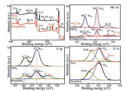
The surface compositions and chemical states of MoS2 and PbS@MoS2 are also investigated by XPS, and the results are shown in Fig. 2. It can be seen from the XPS survey spectra (Fig. 2a), Mo, S, O, C and Pt elements are detected in MoS2 spectrum, while Pb element from PbS can be observed in PbS@MoS2 spectrum besides the elements containing in MoS2 spectrum. Here, C 1s peak at 284.8 eV is used to calibrate all the values of binding energy [23], and Pt peak is attributed to the experimental substrate. Moreover, the high-resolution XPS spectra of the Mo 3d, S 2p and O 1s are further measured and shown in Figs. 2b–d. As depicted in the MoS2 spectrum (Fig. 2b), two peaks with high intensity at 232.75 eV and 229.5 eV can be respectively assigned to Mo 3d3/2 and Mo 3d5/2, corresponding to the Mo4+ state in MoS2 [24]. While the peak with low intensity at 235.8 eV (marked in red) is ascribed to +6 oxidation state of the Mo element (Mo6+ 3d3/2), indicating that a small amount of MoO3 might be contained in the MoS2 sample [25]. The existence of Mo in +6 oxidation state is mainly attributed to partial oxidation of the pure MoS2. Nevertheless, the Mo6+ oxidation state cannot be observed in the PbS@MoS2 spectrum, indicating that the modification with PbS can effectively suppress the oxidation of MoS2, which is consistent with our previous work reports [7]. Besides, there also are two S 2s peaks in the PbS@MoS2 spectrum of Mo 3d, which are ascribed to the S2- state of PbS (marked in red) and the S2- state of MoS2 respectively [26, 27], which suggests that the existence of PbS@MoS2 composites. This can also be further confirmed from the spectra of S 2p. As shown in Fig. 2c, the main peaks at 162.4 eV and 163.8 eV could be attributed to the binding energies of S2- 2p3/2 and S2- 2p1/2 from the MoS2 respectively [28, 29], while the peak of PbS@MoS2 spectrum located at lower binding energies located (161.15 eV) could be assigned to S2- 2p3/2 from the PbS [30]. It can be concluded from Figs. 2b and c, when the MoS2 nanosheets are modified by PbS, the corresponding peaks of Mo 3d and S 2p slightly shift to the higher binding energy compared with the pure MoS2, illustrating that the electronic transfers from MoS2 to PbS [31]. As shown in the high-resolution spectra of O 1s (Fig. 2d), the peaks near 532 eV and 533.7 eV are observed in both MoS2 and PbS@MoS2 spectrum, which can be attributed to surface adsorbed oxygen atoms (Oad) and hydroxyl groups (O-H) respectively [32, 33]. It should be pointed out that the peak of lattice oxygen (Olattice) located at 530.9 eV [34] is presented in the MoS2 spectrum only, and does not observe in the PbS@MoS2 spectrum, which further confirms that the modification of PbS can effectively suppress the oxidation of MoS2.

|
Download:
|
| Fig. 2. (a) XPS spectra of pure MoS2 and PbS@MoS2 composites. High-resolution XPS spectra of (b) Mo 3d, (c) S 2p and (d) O 1s. | |
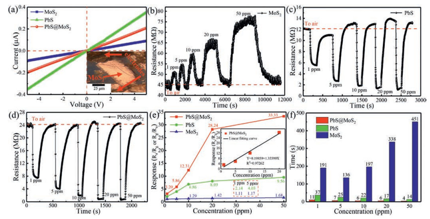
In order to investigate the gas sensing performance of asprepared MoS2, PbS and PbS@MoS2 gas sensors, the I-V characteristic curves of these three gas sensors in air atmospheres are measured firstly. As depicted in Fig. 3a, all the three sensors manifest the clearly linear I-V relationship under the applied voltages range from -5 V to +5 V, indicating that the typical ohmic contacts are formed between the sensing materials and electrodes. Besides, as demonstrated in the optical image of the gas sensor (the inset of Fig. 3a), the sensing materials (PbS@MoS2) are bridged between the adjacent electrodes to form current conductive pathway. Thus, it can be concluded that the forthcoming gas sensing behaviors are dominantly determined by the sensing materials [35]. The dynamic response curves of MoS2, PbS and PbS@MoS2 gas sensors upon exposure to different concentrations of NO2 (ranging from 1 ppm to 50 ppm) are further studied and shown in Figs. 3b–d. For the MoS2 based gas sensor as revealed in Fig. 3b, the resistance gradually increases along with the increase of NO2 concentrations, exhibiting n-type response behavior. When the MoS2 gas sensor is exposed to NO2, the gas molecules adsorb on the surface of MoS2 in the form of physisorption and capture electrons from MoS2 to form an electric dipole moment [13]. In addition, a small amount of NO2 molecules adsorb chemically on the surface of MoO3, and thus taking electrons from the surface of materials. It should be pointed out that both MoS2 and MoO3 are ntype semiconductors, the electrons transfer from sensing materials to NO2 molecules lead to a decrease in the carrier concentration of sensing materials, resulting in an increase in the resistance of the sensor. On the contrary, due to PbS is a p-type semiconductor, the resistance of PbS gas sensor decreases after exposure to NO2 as shown in Fig. 3c [36, 37]. As observed in Fig. 3d, the response behavior of PbS@MoS2 gas sensor is consistent with that of PbS gas sensor. As for the hybrid system based on PbS@MoS2 composites, the adsorption energy of NO2 on the PbS is significantly larger than that on MoS2 [7], which means that NO2 gas molecules is more easily adsorbed on the surface of PbS rather than MoS2 surface. When PbS@MoS2 composite is exposed to the NO2, PbS particles play the role of the sensitive core during the gas sensitive reaction. Thus, PbS@MoS2 gas sensor exhibits p-type response behavior toward NO2, which is similar to that of PbS based gas sensor. To further investigate the effect of PbS modification on the sensing properties, the response values and the response times of the three gas sensors are examined upon exposure of NO2 over a range of 1- 50 ppm at room temperature. As shown in Fig. 3e, it can be clearly observed that the response values of all gas sensors increase with the increase of NO2 concentration. In comparison with the pure MoS2 and PbS gas sensors, PbS@MoS2 gas sensor exhibits the highest response value and the best sensitivity toward NO2 in the whole test range, indicating that the modification of PbS can effectively enhance the NO2 sensing properties. Furthermore, it can be found that, as depicted in the inset of Fig. 3e, the correlation coefficient (R2) of the response value fitting curve for PbS@MoS2 gas sensor at 1-20 ppm NO2 is 0.973, indicating that the response values of PbS@MoS2 gas sensor are of good linearity in the range of 1–20 ppm. The response times of three sensors exposed to 1- 250 ppm NO2 are summarized and shown in Fig. 3f. It is clear that the response time of PbS@MoS2 gas sensor is significantly decreased compared with the other two sensors, which is reduced by two orders of magnitude, from hundreds of seconds to less than ten seconds, implying that the gas sensor based on PbS@MoS2 composites exhibits excellent response speed towards NO2. On the basis of the above results, it can be confirmed that the sensor based on PbS@MoS2 composites exhibits excellent NO2 sensing performance compared with the pure MoS2 and PbS gas sensors, including higher response value, better sensitivity and faster response speed.

|
Download:
|
| Fig. 3. (a) I-V characteristic curves of PbS, MoS2 and PbS@MoS2 gas sensors in air atmospheres. The inset is the optical image of PbS@MoS2 gas sensor. Dynamic response curves of (b) MoS2, (c) PbS and (d) PbS@MoS2 gas sensors at different NO2 concentrations. (e) Response value versus NO2 concentrations curves of MoS2, PbS and PbS@MoS2 gas sensors. The inset shows the linear fitting curve of PbS@MoS2 gas sensor to 1-20 ppm NO2. (f) Comparison diagram of response time for MoS2, PbS and PbS@MoS2 gas sensors. | |
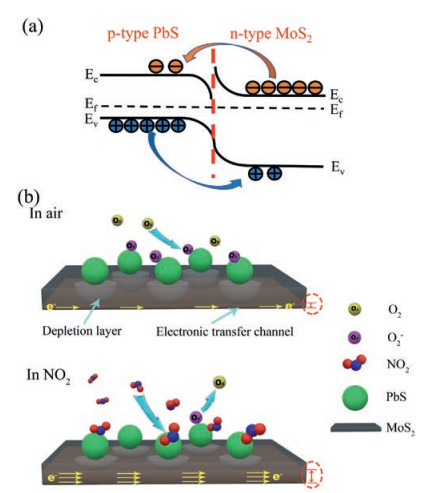
To achieve a better understanding of gas-sensing mechanism of PbS@MoS2 against NO2, the energy band diagram is presented in Fig. 4a. As for the hybrid system based on PbS@MoS2 composites, considering that the Fermi levels of n-type MoS2 is higher than that of p-type PbS, the electrons in MoS2 tend to diffuse into PbS while the holes in PbS will transfer to MoS2 until the system realize the equalization of the Fermi level. This process leads to the formation of depletion layers at the interface between MoS2 and PbS, namely, the formation of p-n heterojunction [38]. Besides, the change of depletion layers during NO2 adsorption and desorption is illustrated in Fig. 4b. When the PbS@MoS2 gas sensor is exposed to NO2, the NO2 molecules adsorbed on the surface of PbS act as the electron acceptors and capture electrons from PbS nanoparticles [39], which results in the increase of hole concentration in PbS. Owing to the electron transfer process, the width of the depletion layer gets thinner when exposure to NO2 [40-42], so that the measured resistance is decreased and the PbS@MoS2 gas sensor exhibits the p-type response characteristic, which is the same as the PbS sensor. Based on the above gas-sensing mechanism, mechanically exfoliated MoS2 nanosheets and PbS particles are chosen to construct the heterostructure, which provides the basis for PbS@MoS2 composite to have excellent gas sensing properties. PbS particles served as the active gas sensing sites interact directly with NO2, which effectively regulates the width of the depletion layer between PbS and MoS2. Meanwhile, MoS2 nanosheets acted as the dominant conductive channel are greatly affected by the variation in width of the depletion layer due to the thin thickness of MoS2, and the whole electron transport channel can be controlled maximumly along with the modulation of the depletion layer during the NO2 adsorption and desorption processes. Additionally, different from fluffy ball-like MoS2 in previous work [7], the flake-like MoS2 nanosheets can provide abundant and effective attachment plat-forms for PbS particles, contributing to the formation of more active sites. In brief, benefited from the effective modulation of the conductive channel and the increased active sites, PbS@MoS2 gas sensor reveals the higher response value and better sensitivity. On the other hand, the outstanding response speed may be ascribed to the following factors. Considering that the NO2 molecules are more inclined to adsorb physically on the surface of the mechanically exfoliated MoS2 [43, 44], which means that more time is demanded to reach the dynamic equilibrium state, so the response process of MoS2 gas sensor is relatively slow. While NO2 is adsorbed on the PbS surface in the form of chemisorption [36, 37], which is a fast process and results in shorter response times for PbS sensor. That is the reasonwhy the response speedof thePbS sensor is faster comparable to that of the MoS2 gas sensor in our experiment. However, the response time of pure PbS sensor is slightly longer than that of PbS@MoS2 sensor, because pure PbS particles have a tendency to agglomerate, resulting in the relatively slow diffusion of target gas in the dense agglomerated particles. It is worthwhile noting that, as for the PbS@MoS2 based gas sensor, the flake-like MoS2 nanosheet with large surface area offers an ideal surface for attaching the PbS particles, that not only effectively prevents the agglomeration but also constructs many more effective contact sites for NO2 molecules, which could accelerate the process of adsorption reaction. Accordingly, the response speed of MoS2 would be promoted significantly through being modified by PbS.

|
Download:
|
| Fig. 4. (a) Energy band diagram. (b) Change of depletion layers during the NO2 adsorption and desorption. | |
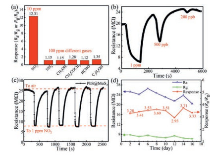
As is well-known, selectivity is indispensable for the practical application of gas sensors. Thus, the response values of PbS@MoS2 sensor toward various gases such as NH3, CH3OH, CH3COCH3, HCHO and C2H5OH are measured. As revealed in Fig. 5a, the response value of PbS@MoS2 sensor to 10 ppm NO2 is remarkably higher than that to 100 ppm other gases, indicating that the PbS@MoS2 sensor exhibits an excellent selectivity towards NO2. As with the selectivity, the detection range of the sensor is also usually used as an important parameter to evaluate gas-sensing performance. Therefore, the NO2 detection limit of PbS@MoS2 gas sensor is further investigated and shown in Fig. 5b. The results manifest that the sensor can still present response behavior even exposed to 200 ppb NO2. According to the 'Air Quality Criteria' published by WHO, NO2 in concentrations above 270 ppb may cause acute health problems in humans. Accordingly, PbS@MoS2 gas sensor can be expected to meet the needs of early warning about acute health problems caused by NO2. Besides, five response/recovery cycles are measured by repeatedly switching the sensor between 1 ppm NO2 and the air atmosphere to investigate the repeatability of PbS@MoS2 gas sensor (Fig. 5c). It can be observed that the resistance of PbS@MoS2 sensor always stays stable either in air or NO2 atmospheres. Meanwhile, the response time and recovery time are almost the same for all cycles, indicating that PbS@MoS2 sensor exhibits satisfactory reversibility and repeatability. Moreover, as illustrated in Fig. 5d, the resistance of PbS@MoS2 sensor exhibits small drifts in both air and 1 ppm NO2 for 16 days, meaning that PbS@MoS2 sensor presents a stabilized sensing performance. The above results indicate that the gas sensor based on PbS@MoS2 composites is of good reliability and manifests potential promising prospect for NO2 detection at room temperature.

|
Download:
|
| Fig. 5. (a) Selectivity of PbS@MoS2 gas sensor to different gases. (b) NO2 detection limit of PbS@MoS2 gas sensor. (c) Repeatability of PbS@MoS2 gas sensor on successive exposure to 1 ppm NO2. (d) Stability of PbS@MoS2 gas sensor to 1 ppm NO2 for 16 days. | |
In summary, PbS@MoS2 composites are successfully synthesized via combining the mechanical exfoliation method with the facile wet-chemical precipitation. As compared with pure MoS2 and PbS, PbS@MoS2 gas sensor exhibits outstanding sensing performances toward NO2 at room temperature, such as high response value, fast response behavior, favorable repeatability and long-term stability. The enhanced gas sensing properties of PbS@MoS2 sensor could be attributed to the synergistic effects between n-type MoS2 nanosheets and p-type PbS particles, including the effective modulation of the conductive channel, the increased active sites and the approximate defect-free surface of mechanically exfoliated MoS2. The experiments demonstrate that the construction of heterostructures for mechanically exfoliated MoS2 will be a promising strategy to improve the sensing properties, which offers useful guidance for designing high-performance MoS2 based gas sensors.
Declaration of competing interestThe authors declare that they have no known competing financial interests or personal relationships that could have appeared to influence the work reported in this paper.
AcknowledgmentsThis work is supported by Hunan Provincial Natural Science Foundation of China (No. 2018JJ2404), Scientific Research Foundation of Hunan Provincial Education Department (Nos. 19A475, 19C1739) and Hunan Science and Technology Plan Program (No. 2019RS1056).
| [1] |
X.H. Liu, T.T. Ma, N. Pinna, J. Zhang, Adv. Funct. Mater. 27 (2017) 1702168. DOI:10.1002/adfm.201702168 |
| [2] |
K. Lee, R. Gatensby, N. McEvoy, T. Hallam, G.S. Duesberg, Adv. Mater. 25 (2013) 6699-6702. DOI:10.1002/adma.201303230 |
| [3] |
H. Li, Z. Yin, Q. He, et al., Small 8 (2012) 63-67. DOI:10.1002/smll.201101016 |
| [4] |
T.T. Xu, Y.Y. Pei, Y.Y. Liu, et al., J. Alloys Compd. 725 (2017) 253-259. DOI:10.1016/j.jallcom.2017.06.105 |
| [5] |
X. Yu, D. Wang, Y.Q. Wang, J. Yan, X.Y. Wang, Chin. Chem. Lett. (2019). DOI:10.1016/j.cclet.2019.11.032 |
| [6] |
S.M. Cui, Z.H. Wen, X.K. Huang, J.B. Chang, J.H. Chen, Small 11 (2015) 2305-2313. DOI:10.1002/smll.201402923 |
| [7] |
X. Xin, Y. Zhang, X.X. Guan, et al., ACS Appl. Mater. Interfaces 11 (2019) 9438-9447. DOI:10.1021/acsami.8b20984 |
| [8] |
B. Chen, E.Z. Liu, F. He, et al., Nano Energy 26 (2016) 541-549. DOI:10.1016/j.nanoen.2016.06.003 |
| [9] |
S. Zhang, H. Yang, H. Gao, et al., ACS Appl. Mater. Interfaces 9 (2017) 23635-23646. DOI:10.1021/acsami.7b03673 |
| [10] |
D.Z. Wang, Z. Pan, Z.Z. Wu, Z.P. Wang, Z.H. Liu, J. Power Sources 264 (2014) 229-234. DOI:10.1016/j.jpowsour.2014.04.066 |
| [11] |
M.Y. Li, C.H. Chen, Y.M. Shi, L.J. Li, Mater. Today 19 (2016) 322-335. DOI:10.1016/j.mattod.2015.11.003 |
| [12] |
H. Li, J. Wu, Z. Yin, H. Zhang, Acc. Chem. Res. 47 (2014) 1067-1075. DOI:10.1021/ar4002312 |
| [13] |
W. Li, Y. Zhang, X. Long, et al., Sensors 19 (2019) 2123. DOI:10.3390/s19092123 |
| [14] |
Q. Zhang, H. Zhang, M.K. Xu, Z.R. Shen, Q. Wei, Chin. Chem. Lett. 29 (2018) 538-542. DOI:10.1016/j.cclet.2017.09.018 |
| [15] |
C. Li, Z.S. Yu, S.M. Fang, et al., Chin. Chem. Lett. 19 (2008) 599-603. DOI:10.1016/j.cclet.2008.03.032 |
| [16] |
H.Q. Cao, G.Z. Wang, S.C. Zhang, X.R. Zhang, Nanotechnology 17 (2006) 3280-3287. DOI:10.1088/0957-4484/17/13/034 |
| [17] |
J.P. Ge, J. Wang, H.X. Zhang, et al., Chemistry 11 (2005) 1889-1894. DOI:10.1002/chem.200400633 |
| [18] |
M. Shkir, M.T. Khan, A. Khan, et al., Mater. Sci. Semicond. Process. 96 (2019) 16-23. DOI:10.1016/j.mssp.2019.02.020 |
| [19] |
M. Shkir, S. AlFaify, V. Ganeshi, S. Yahia, Solid State Sci. 70 (2017) 81-85. DOI:10.1016/j.solidstatesciences.2017.06.006 |
| [20] |
F. Gode, O. Baglayan, E. Guneri, Chalcogenide Lett. 12 (2015) 519-528. |
| [21] |
T. Guo, L.N. Wang, S. Sun, et al., Chin. Chem. Lett. 30 (2019) 1253-1260. DOI:10.1016/j.cclet.2019.02.009 |
| [22] |
H. Li, Q. Zhang, C.C.R. Yap, et al., Adv. Funct. Mater. 22 (2012) 1385-1390. DOI:10.1002/adfm.201102111 |
| [23] |
Y. Zhang, H.F. Zou, J.F. Peng, et al., Sens. Actuator. B-Chem. 272 (2018) 459-467. DOI:10.1016/j.snb.2018.06.007 |
| [24] |
C.J. Han, Z. Tian, H.L. Dou, X.M. Wang, X.W. Yang, Chin. Chem. Lett. 29 (2018) 606-611. DOI:10.1016/j.cclet.2018.01.017 |
| [25] |
Y.Y. Hu, Y.L. Bai, X.Y. Wu, et al., J. Alloys Compd. 797 (2019) 1126-1132. DOI:10.1016/j.jallcom.2019.05.142 |
| [26] |
J. Muscat, C. Klauber, Surf. Sci. 491 (2001) 226-238. DOI:10.1016/S0039-6028(01)01408-X |
| [27] |
H. Ji, C. Liu, T. Wang, et al., Small 11 (2015) 6480-6490. DOI:10.1002/smll.201502355 |
| [28] |
C.Y. Zhai, M.S. Zhu, D. Bin, et al., J. Power Sources 275 (2015) 483-488. DOI:10.1016/j.jpowsour.2014.11.030 |
| [29] |
X.Y. Lin, J. Wang, Z.Y. Chu, et al., Chin. Chem. Lett. 31 (2020) 1124-1128. DOI:10.1016/j.cclet.2019.07.003 |
| [30] |
O.A. Castelo-González, M. Sotelo-Lerma, J.A. García-Valenzuela, J. Korean Inst. Electr. Electron. Mater. Eng. 46 (2016) 393-400. |
| [31] |
K. Wan, D. Wang, F. Wang, et al., ACS Appl. Mater. Interfaces 11 (2019) 45214-45225. DOI:10.1021/acsami.9b16599 |
| [32] |
Y. Han, D. Huang, Y. Ma, et al., ACS Appl. Mater. Interfaces 10 (2018) 22640-22649. DOI:10.1021/acsami.8b05811 |
| [33] |
H.F. Li, G.Z. Lu, Q.G. Dai, et al., Appl. Catal. B 102 (2011) 475-483. DOI:10.1016/j.apcatb.2010.12.029 |
| [34] |
H. Long, A. Harley-Trochimczyk, T. Pham, et al., Adv. Funct. Mater. 26 (2016) 5158-5165. DOI:10.1002/adfm.201601562 |
| [35] |
H.L. Tai, Z.H. Duan, Z.Z. He, et al., Sens. Actuator. B-Chem. 298 (2019) 126874. DOI:10.1016/j.snb.2019.126874 |
| [36] |
A. Mosahebfard, H.D. Jahromi, M.H. Sheikhi, IEEE Sens. J. 16 (2016) 4174-4179. DOI:10.1109/JSEN.2016.2546966 |
| [37] |
P. Salimi kuchi, H. Roshan, M.H. Sheikhi, J. Alloys Compd. 816 (2020) 152666. DOI:10.1016/j.jallcom.2019.152666 |
| [38] |
X. Gao, F. Li, R. Wang, T. Zhang, Sens. Actuator. B-Chem. 258 (2018) 1230-1241. DOI:10.1016/j.snb.2017.11.088 |
| [39] |
E. Wu, Y. Xie, B. Yuan, et al., ACS Appl. Mater. Interfaces 10 (2018) 35664-35669. DOI:10.1021/acsami.8b14142 |
| [40] |
S.W. Choi, A. Katoch, J.H. Kim, S.S. Kim, ACS Appl. Mater. Interfaces 6 (2014) 17723-17729. DOI:10.1021/am504164j |
| [41] |
D.X. Ju, H.Y. Xu, Q. Xu, et al., Sens. Actuator. B-Chem. 215 (2015) 39-44. DOI:10.1016/j.snb.2015.03.015 |
| [42] |
D. Zhang, C. Jiang, P. Li, Y. Sun, ACS Appl. Mater. Interfaces 9 (2017) 6462-6471. DOI:10.1021/acsami.6b15669 |
| [43] |
S.J. Zhao, J.M. Xue, W. Kang, Chem. Phys. Lett. 595- 596 (2014) 35-42. |
| [44] |
B. Cho, M.G. Hahm, M. Choi, et al., Sci. Rep. 5 (2015) 8052. DOI:10.1038/srep08052 |