 2020, Vol. 31


b School of Material and Chemical Engineering, Zhengzhou University of Light Industry, Zhengzhou 450002, China
Nitrogen dioxide (NO2) is toxic and irritating gas, which comes mainly from motor vehicle exhaust and boiler exhaust emissions. The nervous system and respiratory tract will be visibly impaired when the concentration of NO2 exceeds 3 ppm. In addition, high concentrations of NO2 also have cancer-promoting and carcinogenic effect [1]. In the past decade, the demands for low cost, portable, high sensitivity and low power NO2 sensors have greatly stimulated the research enthusiasm on novel sensing materials [2].
Two-dimensional (2D) materials such as graphene, transition metal disulfide and transition metal carbide (MXene) are considered as the most promising alternative candidate materials for the next generation of gas sensors due to the large specific surface area, unique electronic band structure and low noise for application in devices [3-5]. Molybdenum disulfide (MoS2), as a transition metal disulfide, has not only layered structure similar to graphene, but also adjustable band gap [6, 7], excellent optical and electrical properties [8], which has great potential in the fields of energy storage [9], photocatalysis [10], nano devices [11], gas sensors [12, 13], humidity sensor [14] and so on. Lee et al. prepared twodimensional MoS2 nanosheets by hydrothermal method and found that the sensitivity to NO2 gas was related to the S/Mo precursor ratio [15]. However, they only studied the gas sensitivity of the material to 500 ppm NO2. Kumar et al. developed a vertical arrangement MoS2 flake synthesized by chemical vapor deposition (CVD) and the gas sensor showed high response but low recovery speed to NO2 at room temperature [16]. These results fully demonstrated the potential of MoS2 for NO2 gas detection. However, there are still some problems to be solved for NO2 sensor application: (1) The prepared MoS2 films must be uniform, reliable, and easy to integrate; (2) The MoS2 gas sensors should has excellent selectivity and response/recovery speed to NO2 at room temperature.
Although there are many methods for the preparation of two-dimensional MoS2 [14-18], the existing methods such as hydrothermal and micromechanical exfoliation have poor controllability in growth quality and area [17]. More important, the growth area is small, which cannot guarantee the uniformity of thickness and the consistency of layers in the region [18]. Therefore, there is an urgent need for a simple and effective method to grow two-dimensional MoS2, as well as an economic process for manufacturing highly reliable sensor devices.
In this work, two-dimensional MoS2 film was prepared by sulfuring molybdenum atomic layer on SiO2/Si substrate. The important growth factors such as reaction temperature, heating rate, holding time and carrier gas velocity were regulated in the synthesis process and the quality of MoS2 film was evaluated by optical microscope, atomic force microscope, Raman spectrum and photoluminescence spectrum. In addition, two-dimensional MoS2 gas sensor was fabricated and its gas sensing performance was studied. The results showed that the MoS2 sensor had good gas sensitive response only to ammonia and NO2. In the last, the sensitivity mechanism of the material was explored initially.
Preparation of two-dimensional MoS2 film: The MoS2 film was prepared by a CVD system as shown in the Fig. S1b (Supporting information), which includes gas cylinder, gas path, flow control meter and a single temperature zone tubular furnace. First of all, molybdenum films with the thickness of 1 nm were prepared by electron beam evaporation on 300 nm SiO2/Si substrates. Then, 0.8 g high purity sulfur (99.99%, Aladdin) was ground into powder and laid flat in the porcelain boat as shown in the Fig. S1d (Supporting information). Then, the sulfur was putted in the uptake of the tubular furnace heating zone so that the temperature of the position can be sublimation during the reaction. The Mo/SiO2/Si substrate was placed in the constant temperature area of the tubular furnace. In the preparation, the temperature of tubular furnace during the whole reaction process as shown in the Fig. S1c (Supporting information) was set as follows: In the first stage, the temperature raised from room temperature to 200 ℃; in the second stage, the temperature raised from 200 ℃ to different reaction temperatures; in the third stage, the temperature was kept for heat preservation, the temperature was naturally lowered to room temperature. In the last, MoS2 thin films were prepared. The effects of reaction temperature, heating rate, holding time and carrier gas velocity were studied. The name of samples were defined as "sample a-i" for different preparation conditions as shown in the Table S1 (Supporting information).
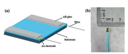
Fabrication and measurement of MoS2 gas sensor: the schematic diagram of the MoS2 gas sensor is shown in Fig. 1a. The Au electrodes were first vacuum evaporation on MoS2 film. Then, the non-conductive AB adhesive coated on Au electrodes to increase its strength and protect electrode. The picture of real products of MoS2 gas sensor could be seen in the Fig. 1b. The resistance of MoS2 has obvious response to light through the previous report, so it was tested to exclude the influence of light by shading aluminum foil out of test chamber. Using static gas testing method, methanol, ethanol, acetone, formaldehyde, ammonia, and nitrogen dioxide were selected test. The gas concentration in the test was 100 ppm.

|
Download:
|
| Fig. 1. (a) diagram of MoS2 gas sensor and (b) picture of real MoS2 gas sensor. | |
The sensitive performance was studied on the CGS-1TP intelligent gas sensitivity analysis system (Beijing Elite Tech Co., Ltd., China). Gas concentration was obtained by static distribution method [19]. In this work, the sensitivity of NO2 is defined as ΔR/Ra×100%, where ΔR = Rg – Ra, Rg and Ra are the resistances of materials in sensitive gas and air. However, the sensitivity of reduction gases such as NH3 is defined as (–ΔR)/Ra×100%. Response/recovery time is defined as the time required when the resistance change reaches 90% of the total change.
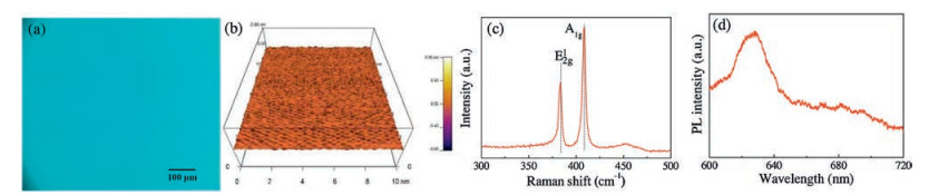
The effect of preparation temperature on MoS2 film growth was studied firstly. The temperatures of tubular furnaces in the preparation were set at 650 ℃, 750 ℃ and 850 ℃ for samples a, b and c, respectively. Figs. S2a-c (Supporting information) were optical microscope (OM) photographs of samples a–c, which could reflect the uniformity of the MoS2 film (Supporting information). In the OM images, the MoS2 film on the SiO2/Si substrate appeared to be blue, and the area without MoS2 appeared purple (Fig. 2a). Obviously, the samples grown at 750 ℃ and 850 ℃ were more uniform in the whole area than the sample grown at 650 ℃. In addition, the surface uniformity of MoS2 film was characterized by atomic force microscopy in Fig. 2b. Obviously, the surface of MoS2 film is very flat and continuous, which facilitates electron transport when used as sensitive material. The quality and layer number of the MoS2 film could be studied by Raman spectra (Fig. 2c and Fig. S3 in Supporting information). Generally, two typical Raman peak, E2g1 in-plane vibration mode and A1g out plane vibration mode were investigated to reflect the crystal structure of MoS2. For the "sample a" as shown in Fig. S3, the E2g1 and A1g were 383.5 cm-1 and 408.1 cm-1, with the peak distance of 24.6 cm-1. As shown in Fig. 2c, the E2g1 and A1g of "sample b" were located at 384.0 cm-1 and 406.6 cm-1 [20], with the peak distance of 22.6 cm-1. As reported, the peak frequency difference between E2g1 and A1g decreased with layer number. Therefore, the MoS2 film prepared at 750 ℃ had more layers then prepared at 650 ℃. In addition, the intensity of "sample b" stronger than that of "sample a", which indicated its higher quality. For the "sample c" prepared at 850 ℃, no Raman peaks were observed, which might be due to the evaporation of sulfur powder too quickly to reaction with Mo on the SiO2/Si. In addition to Raman characteristics, we also investigated the PL properties of the MoS2 films, which could reflect the number of layers, film quality and energy level structure of MoS2 film. As shown in Fig. 2d, the obvious PL peak could be observed in "sample b", but there is no obvious PL peak in other samples (Fig. S4 in Supporting information). Therefore, the 750 ℃ was the best reaction temperature in the preparation of MoS2 film.

|
Download:
|
| Fig. 2. (a) OM image, (b) AFM image, (c) Raman spectra and (d) PL spectra of MoS2 sample (sample b). | |
The effect of holding time on film growth was further investigated with the reaction temperature set as 750 ℃. The holding time of samples d, b and e were 0 min, 30 min and 60 min, respectively. As shown in Figs. S2d, b and e (Supporting information), the MoS2 film was only obtained at the holding time of 30 min. Short holding time means short contact time between S and Mo. However, the long holding time might be led to the excess S deposition on the substrate surface. As shown in Fig. S3, no Raman or PL peaks was observed due to the absence of MoS2. Therefore, 30 min was a suitable holding time.
Then, the effect of heating rate on film growth was also researched. Three different heating rates (3 ℃/min, 25 ℃/min and 40 ℃/min) were set to prepare the MoS2 film. As shown in Figs. S2b, f and g (Supporting information), almost no MoS2 was formed when the heating rate was 3 ℃/min, which due to the sulfur evaporate prematurely and the reaction cannot be carried out. When the heating rate was 40 ℃/min, a rough surface on substrate was observed in the Fig. S2g. It was worth noting that both the Raman and PL peaks were observed. The rough surface on substrate might be because of the violent chemical reaction between sulfur and molybdenum layer. Therefore, 25 ℃/min was a suitable heating rate.
In the last, the carrier gas velocity on MoS2 film growth was investigated. Figs. S2h, i and b are the OM images of MoS2 film prepared under three different carrier gas velocities of 3 sccm, 50 sccm and 100 sccm, respectively. Obviously, all three samples shown similar blue surface. Both Raman and PL spectra proved that these MoS2 films were successfully prepared. The intensities of both Raman and PL peaks increased with the carrier gas velocity. In addition, the Raman peak distance of "sample i" was 23.1, which smaller than that of "sample b". The smaller Raman peak distance might be from the small layer of MoS2 film. Therefore, the faster carrier gas velocity would help to the growth of MoS2 film.
In a short, the optimum synthesis parameters for MoS2 film were heating rate of 25 ℃/min, reaction temperature of 750 ℃, holding time of 30 min and carrier gas velocity of 100 sccm. The surface of the sample obtained under this condition is even, which can be seen from the AFM characterization of "sample b" in Fig. 2b.
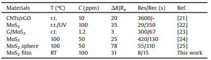
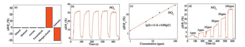
The gas sensing performance of MoS2 gas sensor was tested. As shown in Fig. 3a, 100 ppm of gases which included reducing gases such as ethanol, methanol, acetone, formaldehyde, NH3 and oxidizing gas such as NO2 were tested at room temperature. Interestingly, the MoS2 gas sensor showed good response to NH3 (Fig. S5 in Supporting information) and NO2 and almost no response to other gases, which indicated the good selectivity of the MoS2 gas sensor. The relationship between sensitivity and NO2 concentration was shown in Fig. 3b. The sensitivity of MoS2 gas sensor to 1, 5, 10, 20, 50 and 100 ppm NO2 is 1.2%, 4.2%, 7.0%, 13.0%, 20.9% and 31.3%, respectively. Fig. 3c is a fitting curve of sensitivity and NO2 concentration for MoS2 gas sensor. Obviously, the logarithm of concentration was linear with logarithm of sensitivity. It can be expressed as lg(S) = 0.16 + 0.69lg(C), where S and C represent sensitivity and gas concentration respectively. Furthermore, the dynamic responses of the MoS2 gas sensor was shown in Fig. 3d, which demonstrated the stable sensing recyclability toward NO2 gas. In addition, the response recovery curve of MoS2 gas sensor to NH3 reaction is shown in Fig. S3, the response is about 20, but the recovery time is longer. Compared with other NO2 sensors reported in Table 1 [21-25], the MoS2 gas sensor in this work has great advantages in high NO2 sensitivity, low limit of detection, rapid response/recovery speed and can operation at room temperature.

|
Download:
|
| Fig. 3. (a) Sensitivity of MoS2 to 100 ppm six different gases. (b) Response/recovery curves of MoS2 gas sensor to different concentrations of NO2. (c) Relationships of sensitivity with NO2 concentration. (d) Cyclic stability test of MoS2 sensor to 100 ppm NO2. | |
|
|
Table 1 Recent references about gas sensors for NO2 gas detection. |
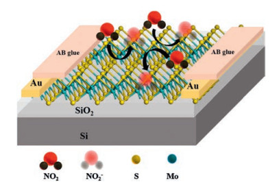
The gas-sensitive mechanism of MoS2 gas sensor could be understood from the structure of MoS2 materials. As shown in Fig. 4, the sulfur atoms are mainly on the outer layer of MoS2. These sulfur atoms are easily to polarize because of the large atom. For the NO2 gas, the electronegativity of O (3.52) is larger than N (3.08), which causes some of positive charge on the nitrogen atom [26]. When NO2 is in contact with MoS2 film, the NO2 will absorbs electrons and becomes NO2- (ads) [27]. As we known, MoS2 is a N-type semiconductor, in which the electrons are the main carriers [12]. The formation of NO2- (ads) will increases the resistance of the MoS2 film, which was very consisted with the result of Fig. 3b. NO2 and adsorbed electrons will react as follows [28].

|

|
Download:
|
| Fig. 4. Schematic of diagram of gas sensitivity mechanism. | |
On the other hand, the electronegativity of H (2.20) is smaller than N (3.08), which causes some of negative charge on the nitrogen atom. The electron of NH3 will transfer to MoS2 film and decrease the resistance. In addition, the MoS2 film synthesized by indirect CVD method is polycrystalline. There are a large number of suspended bonds on the grain boundary surface. These suspended bonds are relatively easy to be absorbed and utilized by NO2, thus making gas sensing properties [29].
In this work, MoS2 films were successfully prepared on SiO2/Si substrates by chemical vapor deposition. The quality of the film was observed by optical microscope, Raman spectra and PL spectra. By studying the control variables, the optimum conditions for the synthesis of MoS2 film were determined. The characterization results showed that the optimum synthesis parameters were heating rate of 25 ℃/min, reaction temperature of 750 ℃, holding time of 30 min and carrier gas velocity of 100 sccm. The MoS2 gas sensor was fabricated and its gas sensing performance was tested. It has good sensitive performance to NO2 gas detection, which include the good selectivity, fast response/ recovery speed and low limit of detection. The sensitivity to 100 ppm of NO2 was 31.3%, and the response/recovery times were 4 s and 5 s, respectively. In addition, the limit of detection could be as low as 1 ppm. The sensitive mechanism is attributed to the structure of the MoS2 material and the electrophilic ability of the NO2 gas.
AcknowledgmentsWe greatly thank the financial supports from the National Natural Science Foundation of China (Nos. 51572173, 51602197, 51771121 and 51702212), Shanghai Municipal Science and Technology Commission (Nos.19ZR1435200, 18511110600 and 19JC1410402), Innovation Program of Shanghai Municipal Education Commission (No. 2019- 01-07-00-07-E00015), Shanghai Academic/Technology Research Leader Program (No. 19XD1422900).
Appendix A. Supplementary dataSupplementary material related to this article can befound, in the online version, at doi:https://doi.org/10.1016/j.cclet.2019.11.032.
| [1] |
N. Joshi, T. Hayasaka, Y. Liu, et al., Mikrochim. Acta 185 (2018) 213. DOI:10.1007/s00604-018-2750-5 |
| [2] |
H.J. Park, W.J. Kim, H.K. Lee, et al., Sens. Actuator. B-Chem. 257 (2018) 846-852. DOI:10.1016/j.snb.2017.11.032 |
| [3] |
L.J. Zhao, K. Wang, W. Wei, et al., Infomat 1 (2019) 407-416. DOI:10.1002/inf2.12032 |
| [4] |
Z.Z. An, Z.G. Li, Y.Y. Guo, et al., Chin. Chem. Lett. 28 (2017) 1492-1498. DOI:10.1016/j.cclet.2017.02.014 |
| [5] |
G. Swain, S. Sultana, J. Moma, et al., Inorg. Chem. 57 (2018) 10059-10071. DOI:10.1021/acs.inorgchem.8b01221 |
| [6] |
H.Y. Chen, J. Wang, L. Meng, T. Yang, K. Jiao, Chin. Chem. Lett. 27 (2016) 231-234. DOI:10.1016/j.cclet.2015.09.018 |
| [7] |
X. Zhou, X. Cheng, Y. Zhu, et al., Chin. Chem. Lett. 29 (2018) 405-416. DOI:10.1016/j.cclet.2017.06.021 |
| [8] |
L. Zhang, X. Ji, X. Ren, et al., Adv. Mater. 30 (2018) e1800191. DOI:10.1002/adma.201800191 |
| [9] |
X. Feng, X. Wang, W. Xing, et al., Compos. Sci. Technol. 93 (2014) 76-82. DOI:10.1016/j.compscitech.2013.11.016 |
| [10] |
P. Li, D. Zhang, J. Wu, et al., Sens. Actuator. A 283 (2018) 34-41. DOI:10.1016/j.sna.2018.09.044 |
| [11] |
S.L. Zhang, H.H. Choi, H.Y. Yue, et al., Curr. Appl. Phys. 14 (2014) 264-268. DOI:10.1016/j.cap.2013.11.031 |
| [12] |
Y. Zhong, W. Li, X. Zhao, et al., ACS Appl. Mater. Interfaces 11 (2019) 13441-13449. DOI:10.1021/acsami.9b01737 |
| [13] |
Y. Wen, F. Wei, W. Zhang, et al., Chin. Chem. Lett. 30 (2019) 10018417. |
| [14] |
Y. Zhang, H. Zou, J. Peng, et al., Sens. Actuator. B-Chem. 272 (2018) 459-467. DOI:10.1016/j.snb.2018.06.007 |
| [15] |
C.M. Lee, C.H. Jin, C.H. Ahn, et al., Phys. Status Solidi A A 216 (2019) 1800999. |
| [16] |
S. Ramu, T. Chandrakalavathi, G. Murali, et al., Mater. Res. Express 6 (2019) 085075. DOI:10.1088/2053-1591/ab20b7 |
| [17] |
S. Li, X. Chen, F. Liu, et al., ACS Appl. Mater. Interfaces 11 (2019) 11636-11644. DOI:10.1021/acsami.9b00856 |
| [18] |
S.K. Kim, R. Bhatia, T.H. Kim, et al., Nano Energy 22 (2016) 483-489. DOI:10.1016/j.nanoen.2016.02.046 |
| [19] |
D. Wang, L. Tian, H. Li, et al., ACS Appl. Mater. Interfaces 11 (2019) 12808-12818. DOI:10.1021/acsami.9b01465 |
| [20] |
D. Wang, Y.Q. Wang, X.D. Chen, et al., Nanoscale 8 (2016) 4107-4112. DOI:10.1039/C5NR05768J |
| [21] |
H.Y. Jeong, D.S. Lee, H.K. Choi, et al., Appl. Phys. Lett. 96 (2010) 213-105. |
| [22] |
R. Kumar, N. Goel, M. Kumar, ACS Sens. 2 (2017) 1744-1752. DOI:10.1021/acssensors.7b00731 |
| [23] |
B. Cho, J. Yoon, S.K. Lim, et al., ACS Appl. Mater. Interfaces 7 (2015) 16775-16780. DOI:10.1021/acsami.5b04541 |
| [24] |
L. Yu, F. Guo, S. Liu, et al., Mater. Lett. 183 (2016) 122-126. DOI:10.1016/j.matlet.2016.07.086 |
| [25] |
Y. Niu, R. Wang, W. Jiao, et al., Carbon 95 (2015) 34-41. DOI:10.1016/j.carbon.2015.08.002 |
| [26] |
I. Jang, H.J. Leong, H. Noh, et al., J. Ind. Eng. Chem. 37 (2016) 380-389. DOI:10.1016/j.jiec.2016.04.002 |
| [27] |
Z.Y. Guo, Y. Zhong, Y. Liu, et al., Chin. Chem. Lett. 28 (2017) 743-747. DOI:10.1016/j.cclet.2016.10.007 |
| [28] |
H. Li, Z. Yin, Q. He, et al., Small 8 (2012) 63-67. DOI:10.1002/smll.201101016 |
| [29] |
M. Ikram, L. Liu, Y. Liu, et al., Nanoscale 11 (2019) 8554-8564. DOI:10.1039/C9NR00137A |