 2020, Vol. 31


b Shanxi Kunming Tobacco Co., Ltd., Taiyuan 030032, China;
c Shanxi Key Laboratory of Gas Energy Efficient and Clean Utilization, Taiyuan 030024, China
Metal oxide semiconductor (MOS) materials have wide applications, including transistors [1], solar cells [2], supercapacitors [3], photocatalysis [4] and sensor fields [5], due to their adjusted band gap, charge carrier mobility, high stability and durability. Nowadays, MOSs including V2O5, ZnO, SnO2 and CuO as sensor materials have been reported and used for the detection of volatile organic compounds (VOCs) [6-11]. Among of them, SnO2 is an important n-type MOS with a wide band gap (3.6 eV) at room temperature, and it has potential application as gas-sensing materials. The SnO2-based sensor can be used to detect many inflammable, explosive gases and VOCs such as methane [11], hydrogen [12], n-butanol [13], acetone [14], toluene [15] and triethylamine [16]. However, pure SnO2 exhibits low response and selectivity, which limits its further application in practice [17]. To improve the gas-sensing properties, more efforts are focused on functionalization [18], doping [19] and composites [20]. Besides mentioned, formation of heterostructures between semiconductors is also an effective strategy [21, 22]. The reported results show that SnO2 heterojunctions including CeO2/SnO2 [17], WO3/SnO2 [23] and CuO/SnO2 [22, 24] play a key role in improvement of gassensing properties.
Among VOCs, triethylamine (TEA) is a volatile and toxic compound and it is released from dead seafood and wastewater. It is also an important raw material of organic synthesis, solvent, polymerization inhibitor, preservative and synthetic dye. Therefore, the detection of TEA is not ignored. When humans and animals are exposed to TEA, it will strongly irritate the respiratory tract of humans and animals, causing nausea, headache, pulmonary edema and even death after inhalation [25]. According to the American Conference of Government Industrial Hygienists (ACGIH), the time-weighted average permissible concentration of TEA in the workplace is 10 ppm and the permissible concentration for short exposure is 15 ppm [16]. Therefore, the development of a novel sensor material with low detection limit, high sensitivity and high selectivity to TEA is necessary to meet demand of TEA monitoring in complex workplaces and to ensure a healthy working and living environment. Du et al. reported that the SnO2 quantum dots and nanospheres can be used for selective detection of low-concentration TEA [9, 26]. Qiao et al. investigated MoS2/SnO2 heterojunction nanomaterial for 5 ppm TEA detection [27]. It is confirmed that copper-modified SnO2 has enhanced chemiluminescence response of H2O2 [28]. However, to the best of our knowledge, 3D laminated of CuO/SnO2 nanomaterial used to detect TEA less than 5 ppm is still rarely reported.
Herein, we provide a simple synthesis route of CuO/SnO2 heterojunction nanomaterial. The structure and morphology were characterized and the sensing properties were also studied.
CuO/SnO2 was synthesized according to the simple strategy (Fig. S1a in Supporting information). Their phase composition and crystal structures were characterized by XRD technique and the results are shown in Fig. S1b (Supporting information). All the diffraction peaks at 26.61°, 33.89°, 37.95°, 51.78° correspond to (110), (101), (200) and (211) crystal planes of tetragonal rutile SnO2, which are well consistent with the standard card (JCPDS No. 41-1445). No other peaks of impurity including CuO crystal phase were detected in the XRD patterns, which may be due to the trace CuO in the CuO/SnO2 materials and/or exceeding the detection limit of XRD [29]. In addition, the high intensities of all diffraction peaks of CuO/SnO2 indirectly indicated the presence of CuO crystal phase, and the increase in crystallinity of SnO2 due to introduction of CuO [30]. In the hydrothermal process, the introduction of dispersed and uniform copper ions promotes the crystallization of SnO2, resulting in high crystallinity of heterogeneous nanomaterials. No significant peak shifts indicate that the CuO and SnO2 crystal phases existed in CuO/SnO2 materials independently, implying a possibility of the formation of p-n heterojunction at the contact interface of two-phase [31].
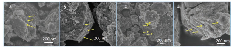
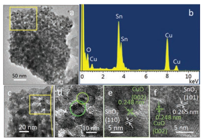
The morphologies of as-synthesized 3D laminated CuO/SnO2-x were shown in Fig. 1. All materials possess similar 3D block microstructure formed by stacked layers, which were selfassembled with nanoparticles. Morphologies are more similar to rock stratum marked with yellow arrows (Figs. 1a–d). Lamellae sizes are in the range of several hundred nanometer. TEM image of CuO/SnO2-3 further confirms that the single lamella was composed of size-uniformed nanoparticles (Fig. 2a), which components contain Sn, Cu and O elements analyzed by EDS spectrum (Fig. 2b and Table S1 in Supporting information). The yellow area marked in Fig. 2a was further observed by HRTEM and image displays in Fig. 2c. Nanoparticles were close packed together and their sizes are ca.10 nm (arrows indication in a square box). The magnification of arrow-indicated area shows that two particles were closely connected and their crystal lattice fringes are also clearly visible (green circles in Fig. 2d). The fine structures of nanoparticles are shown in Figs. 2e and f. The spacings of the lattice fringe are 0.324 and 0.265 nm correspond to (110) and (101) planes of SnO2, respectively. The spacing of 0.248 nm is indexed with (002) plane of CuO crystal. Notably, nanoparticles of heteronuclear fused together are easy to form heterojunction structures, indicating heterojunctions of SnO2 and CuO exist in CuO/SnO2-3 material.

|
Download:
|
| Fig. 1. SEM images of as-synthesized 3D laminated CuO/SnO2 materials: (a) SnO2, (b) CuO/SnO2-1, (c) CuO/SnO2-3 and (d) CuO/SnO2-5. | |

|
Download:
|
| Fig. 2. (a) TEM image, (b) EDS spectrum and (c–f) HRTEM images of as-synthesized 3D laminated CuO/SnO2-3 material. | |
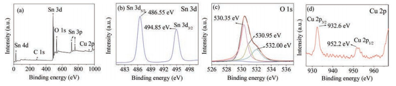
The surface composition and chemical state of CuO/SnO2-3 are shown Fig. 3. Full spectrum shows Sn, Cu, C and O elements existing in CuO/SnO2-3 nanomaterial and no other peaks are found (Fig. 3a). The C 1s peak corresponding to C-C at 284.8 eV is attributed to the adventitious carbon in the material, which is taken as the calibration reference. High-resolution XPS spectra of Sn 3d, O 1s and Cu 2p are shown in Figs. 3b and c. The peaks corresponding to Sn 3d5/2 and Sn 3d3/2 at binding energies of 486.55 and 494.85 eV, respectively, are observed (Fig. 3b), which indicates that Sn exists as Sn4+ in CuO/SnO2-3. The asymmetric O 1s peak in the spectrum can be deconvoluted into three peaks centered at 530.35, 530.95 and 532.00 eV (Fig. 3c). The peak at 530.35 eV corresponds to lattice oxygen of SnO2 and CuO, and the peak at 530.95 eV is assigned to the defect oxygen on the surface of material, whereas the peak at 532.00 eV is generally attributable to the adsorbed and dissociated oxygen species (O2-, O2- or O-) [32]. The peaks at 932.6 and 952.2 eV corresponding to Cu 2p3/2 and Cu 2p1/2 can be observed in the XPS spectrum (Fig. 3d), implying Cu exists as Cu2+ as expected. These results indicate that CuO/SnO2 is composed of CuO and SnO2.

|
Download:
|
| Fig. 3. (a) XPS spectra of the full range spectrum, (b) Sn 3d, (c) O 1s and (d) Cu 2p of CuO/SnO2-3 nanomaterial. | |
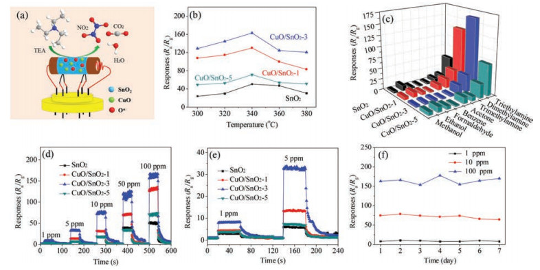
When TEA is injected into the test room, gas molecules reacted with adsorbed oxygen species, resulting in change of resistance, which is behaved as the response to TEA (Fig. 4a). The responses of 3D laminated CuO/SnO2 materials are higher than that of pure SnO2, and CuO/SnO2-3 exhibits highest sensitivity to TEA in the temperatures range of 300–380 ℃ (Fig. 4b). With increasing the working temperature, the gas response curves show a "volcanic" trend, and the responses are dependent on the contents of Cu in Cu:SnO2 materials (Fig. S3b in Supporting information). Therefore, all materials exhibit the maximum response to TEA at 340 ℃, which is mainly ascribed to the influence of temperature on the gas adsorption kinetics of O2 molecules [33]. When the operating temperature is higher than 340 ℃, the adsorption rate tends to be saturated, and the desorption rate increases, resulting in a decrease in the net adsorption rate [34]. Therefore, the gas adsorption and desorption on the surface of CuO/SnO2 materials reach a balance and exhibits excellent sensing performance when the temperature reaches 340 ℃.

|
Download:
|
| Fig. 4. (a) Schematic of gas sensing for TEAdetection. (b) The effectof operating temperatures on response. (c) Selectivity, (d, e) transient response and (f) recoverystability of 3D laminated CuO/SnO2 to TEA. T = 340 ℃. | |
The selectivity was evaluated on exposure to 100 ppm VOCs including methanol, ethanol, formaldehyde, benzene, acetone, triethylamine, dimethylamine and trimethylamine at 340 ℃ (Fig. 4c). Clearly, all CuO/SnO2 materials have a higher response to 100 ppm TEA. Interestingly, the response of CuO/SnO2-3 is much higher, which indicates the high selectivity for detection of TEA. The one reason is that TEA is a stronger reductive gas among VOCs, and thus it reacts with adsorbed oxygen species easily. Additionally, the 3D laminated microstructure, rich mesopores (Fig. S2 in Supporting information) and p-n heterojunction structures contribute to improvement of sensing performance, which can favour more defective oxygen and chemical adsorbed oxygen on the surface of the CuO/SnO2-3 material to act as the active sites for TEA reaction.
The transient profiles are recorded on exposure to TEA with different concentrations (Fig. 4d). The responses increase significantly with increasing TEA concentrations (Fig. S3a in Supporting information). The response-recovery results show that CuO/SnO2 has a fast response time (1 s) and a fast recovery time (ca. 40 s). Notably, CuO/SnO2-3 shows significantly better response to TEA, which are about three-four times as much as that of SnO2. Notably, there are obviously high response to 1 and 5 ppm TEA (Fig. 4e and Fig. S4 in Supporting information). The value reaches 33 (more than five-fold of SnO2) for 5 ppm and is about three times as much as that of SnO2 for 1 ppm TEA, and a fast response and recovery time is 1 and 14 s respectively, which is expected for sensor's application in the detection of extremely low-concentration VOCs. Compared with the reported SnO2 materials modified with oxides and noble metals (Table S2 in Supporting information), the 3D laminated CuO/SnO2-3 is excellent and low-cost sensor material suitable for TEA detection with less than 10 ppm. A linear relationship between response and concentration further confirm that CuO/SnO2-3 has distinctive ability of rapid detection of lowconcentration TEA (Fig. S3a).
The stability was further explored for the detection of 1, 10 and 100 ppm TEA (Fig. 4f). Clearly, CuO/SnO2-3 has high stability in the detection of 1 and 10 ppm TEA, indicating it is an excellent sensor material for detection of extremely low concentration TEA and it has a potential practical application.
The sensing mechanism generally follows the theoryof electron depletion layer [35]. The narrow band gap and thework function of CuO are1.8 and 5.3 eV, respectively, while SnO2 has a bandwidth of 3.6 eV and work function of 4.9 eV at room temperature (Scheme S2 in Supporting information). The p-n heterojunctions can be formed at the phase interface of p-CuO and n-SnO2 by introducing CuO into SnO2 material and it is favour to the balanced of the band gap and Fermi energy level between CuO and SnO2 by adjusting the energy band bending of depletion layers on both sides of the physical interfaces [31]. Thus, a new wide electron depletion layer leads to further increase in resistance, which is important to enhance the sensing performance of CuO/SnO2 material. The surface reaction mechanisms of the 3D laminated SnO2 before and after heterojunction formation are shown in Scheme S3 (Supporting information). When the SnO2-based sensors was exposed to air, oxygen molecules in air adsorbed onto the surfaces of SnO2 or CuO/SnO2 materials, and then captured electrons and form adsorbed ions Oα- (O2-, O- and O2-), leading to the formation of thick electronic depletion layer, making carrier concentration and electron transfer rate decrease, which is behaved as increase in the resistance in air (Ra).
Due to the p-n heterojunction formed by introducing CuO to SnO2, CuO/SnO2 material has a higher resistance resulting from the charge conduction channel narrowed [35]. When CuO/SnO2 was exposed to TEA gas, it reacted with adsorbed oxygen ions resulted from the electron-capturing interaction of n-p transition [36], which decreases the concentration of adsorbed oxygen and the thickness of the electron depletion layer, thus the resistance in TEA (Rg) decreased. The equation is simply described as follows,

|
(1) |
In a word, CuO-doped SnO2 nanpparticles were self-assembled into lamellae with size less than 1 μm and it exhibit enhanced selectivity in the detection of TEA (100 ppm) and obvious sensitivity on exposure toTEA with less than 100 ppm. Particularly, it has a high response and stability to 1 and 5 ppm TEA (S is 8 and 33), which is ascribed to the contribution of 3D laminated structures to sensing properties, more important, the formation of p-n heterojunctionplays a key role due to more adsorbed oxygen on the surface of heterojunctional CuO/SnO2 material, implying 3D laminated CuO/SnO2 material is a potential candidate served as sensor platform for low-concentration TEA detection.
Declaration of competing interestThe authors declare that they have no known competing financial interests or personal relationships that could have appeared to influence the work reported in this paper.
AcknowledgmentsThe authors thank National Natural Science Foundation of China (No. 51572185), Natural Science Foundation of Shanxi Province (No. 2014011016-4) and Key R&D program of Shanxi Province (International Cooperation, No. 201903D421079) for the financial support. This work was also supported by Shanxi Province Technology Foundation for Selected Overseas Chinese Scholar, Research Project Supported by Shanxi Scholarship Council of China, College Student Innovation Program of Shanxi (Nos.2017550, 2018081) and National College Student Innovation and Entrepreneurship Training Program (No. 201910112002).
Appendix A. Supplementary dataSupplementary material related to this article can be found, in the online version, at doi:https://doi.org/10.1016/j.cclet.2020.01.009.
| [1] |
L. Petti, N. Münzenrieder, C. Vogt, H. Faber, et al., Appl. Phys. Rev. 3 (2016) 021303. DOI:10.1063/1.4953034 |
| [2] |
I. Concina, A. Vomiero, Small 11 (2015) 1744-1774. DOI:10.1002/smll.201402334 |
| [3] |
G.C. Li, P.F. Liu, R. Liu, et al., Dalton Trans. 45 (2016) 13311-13316. DOI:10.1039/C6DT01791F |
| [4] |
S. Dursun, I.C. Kaya, V. Kalem, H. Akyildiz, Dalton Trans. 47 (2018) 14662-14678. DOI:10.1039/C8DT02850H |
| [5] |
X. Zhou, X. Cheng, Y. Zhu, et al., Chin. Chem. Lett. 29 (2018) 405-416. DOI:10.1016/j.cclet.2017.06.021 |
| [6] |
D. Meng, J. Si, M. Wang, et al., Chin. Chem. Lett. (2019) doi.org/10.1016/j.cclet.2019.12.021.
|
| [7] |
J. Du, R. Zhao, S. Chen, et al., ACS Appl. Mater. Interfaces 7 (2015) 5870-5878. DOI:10.1021/am509139f |
| [8] |
W. Shi, M.M. Ahmed, S. Li, et al., ACS Appl. Nano Mater. 2 (2019) 5430-5439. DOI:10.1021/acsanm.9b01044 |
| [9] |
J. Du, R. Zhao, Y. Xie, J. Li, Appl. Sur. Sci. 346 (2015) 256-262. DOI:10.1016/j.apsusc.2015.04.011 |
| [10] |
Q. Wang, L. Bao, Z. Cao, Chin. Chem. Lett. (2019) doi.org/10.1016/j.cclet.2019.12.007.
|
| [11] |
C. Su, L. Zhang, Y. Han, et al., Sens. Actuator. B-Chem. 304 (2020) 127347. DOI:10.1016/j.snb.2019.127347 |
| [12] |
A. Katoch, Z. Ul Abideen, H.W. Kim, S.S. Kim, ACS Appl. Mater. Interfaces 8 (2016) 2486-2494. DOI:10.1021/acsami.5b08416 |
| [13] |
Y. Wang, Y. Zeng, L. Wang, et al., Sens. Actuator. B-Chem. 283 (2019) 693-704. DOI:10.1016/j.snb.2018.12.016 |
| [14] |
D. Chen, J. Xu, Z. Xie, G. Shen, ACS Appl. Mater. Interfaces 3 (2011) 2112-2117. DOI:10.1021/am2003312 |
| [15] |
T. Kida, T. Doi, K. Shimanoe, Chem. Mater. 22 (2010) 2662-2667. DOI:10.1021/cm100228d |
| [16] |
Y. Xie, J. Du, R. Zhao, H. Wang, H. Yao, J. Environ. Chem. Eng. 1 (2013) 1380-1384. DOI:10.1016/j.jece.2013.08.021 |
| [17] |
J. Liu, M. Dai, T. Wang, et al., ACS Appl. Mater. Interfaces 8 (2016) 6669-6677. DOI:10.1021/acsami.6b00169 |
| [18] |
Y.J. Jeong, W.T. Koo, J.S. Jang, et al., Nanoscale 10 (2018) 13713-13721. DOI:10.1039/C8NR03242D |
| [19] |
G. Qin, F. Gao, Q. Jiang, et al., Phys. Chem. Chem. Phys. 18 (2016) 5537-5549. DOI:10.1039/C5CP07174G |
| [20] |
Z. Wang, S. Gao, T. Fei, S. Liu, T. Zhang, ACS Sens. 4 (2019) 2048-2057. DOI:10.1021/acssensors.9b00648 |
| [21] |
L. Zhu, K. Yuan, J. Yang, et al., Sens. Actuator. B-Chem. 290 (2019) 233-241. DOI:10.1016/j.snb.2019.03.092 |
| [22] |
J.M. Walker, S.A. Akbar, P.A. Morris, Sens. Actuator. B-Chem. 286 (2019) 624-640. DOI:10.1016/j.snb.2019.01.049 |
| [23] |
D. Xue, Y. Wang, J. Cao, G. Sun, Z. Zhang, Talanta 199 (2019) 603-611. DOI:10.1016/j.talanta.2019.03.014 |
| [24] |
L. He, Y. Jia, F. Meng, M. Li, J. Liu, J. Mater. Sci. 44 (2009) 4326-4333. DOI:10.1007/s10853-009-3645-y |
| [25] |
W. Li, H. Xu, T. Zhai, et al., J. Alloys. Compd. 695 (2017) 2930-2936. DOI:10.1016/j.jallcom.2016.11.380 |
| [26] |
J. Du, S. He, R. Zhao, et al., Mater. Lett. 186 (2017) 318-321. DOI:10.1016/j.matlet.2016.10.046 |
| [27] |
X.Q. Qiao, Z.W. Zhang, D.F. Hou, et al., ACS Sustain. Chem. Eng. 6 (2018) 12375-12384. DOI:10.1021/acssuschemeng.8b02842 |
| [28] |
C. Vakh, A. Pochivalov, A. Podurets, et al., Analyst 144 (2018) 148-151. |
| [29] |
P. Mahmoudi, A. Nemati, M. Maleki Shahraki, J. Alloys. Compd. 770 (2019) 784-791. DOI:10.1016/j.jallcom.2018.08.201 |
| [30] |
L. Li, C. Zhang, W. Chen, Nanoscale 7 (2015) 12133-12142. DOI:10.1039/C5NR02334C |
| [31] |
S. Bai, C. Liu, R. Luo, A. Chen, Appl. Surf. Sci. 437 (2018) 304-313. DOI:10.1016/j.apsusc.2017.12.033 |
| [32] |
G. Li, X. Wang, L. Yan, et al., ACS Appl. Mater. Interfaces 11 (2019) 26116-26126. DOI:10.1021/acsami.9b08408 |
| [33] |
N. Joshi, L.F. da Silva, H.S. Jadhav, et al., Sens. Actuator. B-Chem. 257 (2018) 906-915. DOI:10.1016/j.snb.2017.11.041 |
| [34] |
H. Zhang, W. Shi, N. Gao, et al., Sens. Actuator. B-Chem. 296 (2019) 126633. DOI:10.1016/j.snb.2019.126633 |
| [35] |
H. Li, S. Chu, Q. Ma, et al., ACS Appl. Mater. Interfaces 11 (2019) 8601-8611. DOI:10.1021/acsami.8b22357 |
| [36] |
X. Xin, Y. Zhang, X. Guan, et al., ACS Appl. Mater. Interfaces 11 (2019) 9438-9447. DOI:10.1021/acsami.8b20984 |