 2020, Vol. 31


b State Key Lab of Transducer Technology, Shanghai Institute of Microsystem and Information Technology, Chinese Academy of Sciences, Shanghai 200050, China
Hydrogen sulfide (H2S) is a kind of colorless, flammable, highly fat-soluble and highly corrosive toxic gas. It is also easily produced as a by-product in many industries, such as petroleum refining, aquaculture, waste management and natural gas production. H2S molecules can pass through the cell membrane and prevent cell respiration. If its concentration reaches ppm level, the exposed H2S gas could cause damage to human nervous system [1]. More seriously, it would be fatal in a short time if a person inhales a small amount of high-concentration H2S [2]. Therefore, it is important to accurately and real-time detect H2S gas.
The sensors based on semiconductor metal oxides, such as Co3O4 [3], ZnO [4, 5], SnO2 [6], WO3 [7-9], TiO2 [10] and In2O3 [11], have been widely used for the detection of toxic and inflammable gas, due to their stable properties, low cost, micro size and high compatibility with microelectronic fabrication processes. Among the variable types of metal oxides sensing materials, ZnO has attracted intensive research due to its advantageous properties, such as high mobility of conductive electrons and good chemical/ thermal stability.
The sensing mechanism of ZnO chemiresistive sensors for detecting a reducing gas is usually described by surface depletion model [12]. When the reducing gas (e.g., H2S) is introduced, it reacts with the ionized oxygen species of O2-, O- and O2- that are already formed when ZnO is exposed to oxygen-containing air. The interaction reduces the depletion layer thickness of the ZnO-NWs by releasing electrons back to the conduction band, resulting in decrease of measured resistance and electric sensing signal. Unfortunately, due to the low sensitivity of intrinsic ZnO, high working temperature (300 ℃ or higher) is usually required, which significantly increases power consumption and shortens sensing lifetime. In order to enhance the sensing performance of ZnObased sensor, some efforts, such as changing the surface energy of chemisorption and increasing the conductivity of ZnO, are often made through doping active metal into ZnO or modifying ZnO with active metal oxide. Jaehyun Kim et al. [13] used a photochemical method to deposit CuO on ZnO nanorods for preparing CuO-ZnO nano-sensors. Although CuO-ZnO has enhanced sensitivity to 50 ppm H2S, the required operating temperature is as high as 500 ℃. Sugato Ghosh et al. [14] reported a ZnO/γ-Fe2O3 heterostructure prepared by using a facile single step electrochemical process. In this way an excellent selectivity to H2S was observed, but only two kinds of interference gases (CH4 and CO) were measured to show inadequate selectivity. Weili Zang [15] demonstrated that the sensitivity of an In2O3-ZnO nano-sensor is much higher than that of bare ZnO nano-arrays. Unfortunately, the sensor showed poor sensitivity to low-concentration H2S gas. Therefore, it is necessary to explore new sensing materials in ZnObased gas sensors for higher sensitivity, better selectivity and lower sensor working temperature.
Our previous research established a new H2S sensing effect with ZnO nanowires (NWs) as sensing material [16], which is verified being sulfurized by H2S to form ZnS and the ZnS can be later desulfurized back to ZnO by ambient oxygen. The metastable ZnS intermediate is found at the surface of ZnO-NWs by sulfuration reaction with the targeted H2S. It is the existence of metastable ZnS that causes high H2S sensing signal. Many researches have also proved that it is an effective way to improve the sensitivity of sensor by modifying the surface of sensitive material to form heterojunction [17, 18]. Inspired by this previous research result, this work use ZnS to modify ZnO-NWs to form ZnO-ZnS nanoheterostructures at the surface of the material. The purpose is to adjust energy-band structure by the interaction of ZnS and ZnO, so as to improve material sensitivity to H2S. The detailed study on the influence of the modified ZnS contents to H2S sensing performance has been carried out at various temperatures to achieve optimal sensing material. The results of the study reveal that, comparing with the pure ZnO-NWs, the introduction of ZnS can not only enhance the sensitivity ZnO-NWs but also effectively reduce the working temperature. A possible sensing enhancement mechanism of the sensing-material is also proposed.
Vertically aligned ZnO-NWs for gas sensors were grown on the sensor chip by a two-step hydrothermal method. First, 0.0110 g of Zn(CH3COO)2·2H2O (AR, Aldrich) was dissolved to form a seed solution in 10 mL of C2H5OH (AR). The micro-sensor chip was washed with ethanol and deionized water for 3 min. After drop-wise coating of the seed solution in the comb-finger electrode region of the micro-sensor chip, the chip was dried in air for 10 s and was repeated this coating step for three to four times. Then the chip together with the seed solution was heated in a tube furnace at 350 ℃ for 20 min so as to form a ZnO seed layer. A precursor solution was prepared by dissolving 50 mmol/L HMTA (C6H12N4, AR, Aldrich) and 50 mmol/L Zn(NO3)2·6H2O (AR, Aldrich) in 250 mL deionized water. The chip with the ZnO seed crystal layer was suspended face down on the surface of the precursor solution and sealed at 90 ℃ for 12 h for ZnO growing. Finally, the sensor chip with the grown ZnO-NWs was taken out for gas sensing or further heterojunction formation.
The chips with ZnO-NWs were immersed in 5, 10, 15 and 20 mmol/L Na2S·9H2O (AR, Aldrich) solutions, respectively. After reaction at 70 ℃ for one hour, the sensor chips were taken out from the solutions, washed for three times in ethanol and deionized water alternately, air-dried and labeled ZnO-ZnS-x (x = 5, 10, 15, 20) for sensing experiments.
The structure of the micro-sensor chip and its SEM image are shown in Fig. 1. The fabrication process of the micro-sensor chip can be found in reference [19]. The sensor chip is comprised of comb-finger electrodes, isolation layer, polysilicon heater and suspended silicon nitride support layer. The suspension plate is connected to four narrow support beams that are clamped to the silicon substrate. The chip has four interconnecting pads, two for heating and two for chemiresistive signal readout.

|
Download:
|
| Fig. 1. (a) Schematic of the micro-sensor chip. (b) SEM of the fabricated microsensor chip. (c) The sensor chip with ZnO nanowires grown. | |
Fig. 2a shows the uniform and dense ZnO-NWs in situ synthesized by hydrothermal method. It can be observed from Figs. 1c and 2a that the interspace between a pair of comb-finger electrodes is fully filled up by the densely arrayed ZnO-NWs, with the average diameter about 150 nm. The adjacent nanowires crosslinking to each other form chemiresistor. The nanowires show regular hexagonal cross-section and clear ridge line.

|
Download:
|
| Fig. 2. SEM images of the material samples: (a) ZnO-NWs, (b) ZnO-ZnS-5, (c) ZnO-ZnS-10, (d) ZnO-ZnS-15 and (e) ZnO-ZnS-20. | |
The prepared ZnO-ZnS-x heterostructures are shown in Fig. 2b for x = 5, in Fig. 2c for x = 10, in Fig. 2d for x = 15 and in Fig. 2e for x = 20, respectively. Compared with the ZnO-NWs, the crosssection edges and ridges of the ZnO-ZnS-x (x = 5, 10, 15, 20) heterostructures become more and more blurred along with the Na2S concentration increase. This is attributed to the ion exchange reaction between ZnO and Na2S in solution, resulting in a growing amount of ZnS (Reaction 1).
|
(1) |
The XRD pattern (Fig. 3a) of ZnO is consistent with the standard JCPDS card No. 36-1451 of ZnO, indicating the high crystallinity of the ZnO-NWs. The diffraction peak at 34.5° confirms the perfect (002) ZnO crystal and no other diffraction peaks from impurities are detected. The diffraction peak at 69.5° in the other four XRD patterns shows the presence of ZnS crystal with preferred (201) crystal (JCPDS No. 12-0688). Along with the x increasing, the ratio of the diffraction peak intensity between ZnS (201) and ZnO (002) becomes larger and the diffraction peak of ZnS does not shift. These phenomena indicate that the amount of ZnS modified on the surface of ZnO increases and the crystal structure of ZnS is unchanged during the change of the ZnS amount. Figs. 3b and c is the EDS diagram of ZnO-NWs and ZnO-ZnS-10. Both ZnO-NWs and ZnO-ZnS-x contain O, Zn, and Si, there Si element comes from the silicon substrate of the sensor chip. The S element is found existing in all the ZnO-ZnS-x samples, with its atom percentage (at%, except Si) is 1.28%, 1.72%, 2.52% and 3.00% for x = 5, 10, 15, 20, respectively. In combination with Figs. 2 and 3, it can be concluded that ZnS has been successfully modified on the surface of ZnO-NWs, and the amount of ZnS increases with increasing x.

|
Download:
|
| Fig. 3. (a) XRD pattern of the ZnO-NWs and ZnO-ZnS-x. (b, c) EDS spectrum of ZnO-NWs and ZnO-ZnS-10. | |
The response curves of the ZnO-NWs and the ZnO-ZnS-10 sensors to 1-5 ppm H2S at 300 ℃ have been experimentally obtained, as is shown in Fig. 4. For a kind of reducing gas such as H2S, the sensing response can be expressed as ∆R/R=(RairRgas)/Rair, where Rgas and Rair represent the measured resistance in target gas and clean air, respectively. As is expected, after ZnS modified on the ZnO-NWs surface, the ZnO-ZnS-10 sensor exhibits larger sensitivity than ZnO-NWs sensor, and its response value increases with H2S gas concentration.

|
Download:
|
| Fig. 4. Response of (a) ZnO-NWs and (b) ZnO-ZnS-10 micro-sensors to 1-5 ppm H2S at 300 ℃. | |
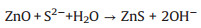
The sensing properties of the ZnO-ZnS-x (x = 5, 10, 15, 20) and ZnO-NWs micro-sensors to 5 ppm H2S are measured at different temperatures (Fig. 5). The sensing results of all the ZnO-ZnS-x (x = 5, 10, 15) and ZnO-NWs sensors show a similar changing rule in terms of the working temperature change. Along with the temperature increase from 100 ℃ to 300 ℃, their response values increase and the highest sensitivity is achieved at about 300 ℃. The main reason lies in that, ata suitable temperature range the electrons transformation from ZnO to the adsorbed oxygen will be promoted to generate more O2- on the surface of ZnO. When H2S gas is introduced to react with the oxygen anion, more electrons are released back to ZnO that results in great resistance decrease and high sensitivity. However, when the operating temperature is further increased up to 400 ℃, the desorption of a large amount of adsorbed oxygen on the surface of ZnO leads to a sharp decrease in the response value to H2S gas.

|
Download:
|
| Fig. 5. Sensing properties of sensors to 5 ppm H2S at various temperatures: (a) the ZnO-ZnS-x (x = 5, 10, 15, 20) and the ZnO-NWs sensors; (b) the ZnO-ZnS-10 and the ZnONWs sensors. | |
It is worth pointing out that the response value of ZnO-ZnS-x (x = 5, 10, 15) is significantly higher than that of ZnO-NWs, especially in the low temperature range (< 300 ℃). The lower the temperature drops, the greater the response increase for the ZnO-ZnS-x sensors. Among the three ZnO-ZnS-x (x = 5, 10, 15) sensors, the ZnO-ZnS-10 sensor has the highest sensitivity within the whole temperature range from 100 ℃ to 400 ℃. Then the followed one is the ZnO-ZnS-15 sensor. For the pure ZnO-NWs, when the operating temperature changes from 300 ℃ to 100 ℃, the response value decreases from 0.78 to 0.12, i.e., it reduces by 84.5%. In contrast, the ZnO-ZnS-10 reduces by only 32.9% (from 0.88 to 0.59). These results show that the ZnO-ZnS heterojunction enhanced sensor is more suitable than the ZnO-NWs sensor for working at low temperature. However, the ZnO-ZnS-20 microsensor has almost no response to H2S gas. This ultra-low response may be attributed to the high content of ZnS that forms a continual and thick ZnS shell to cover the ZnO surface. The whole ZnS coating completely prevents both the reaction of H2S with ZnO and the adsorbed oxygen obtaining electrons from ZnO. Therefore, modifying ZnO-NWs with a suitable amount of ZnS can significantly improve the sensitivity of ZnO-NWs to H2S, especially at low working temperature. Achieving high sensitivity at low temperature facilitates to reduce power consumption and extend the sensor's lifetime.
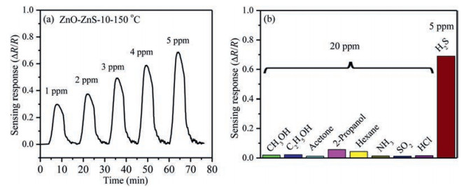
As is shown in Fig. 6a, the ZnO-ZnS-10 micro-sensor exhibits high sensitivity to 1-5 ppm H2S at 150 ℃. Its power consumption is determined to be only 14 mW when it operates at 150 ℃. Good reproducibility of the sensing response is also confirmed by repeatedly detecting 5 ppm H2S gas for five times at 150 ℃ (Fig. S1 in Supporting information), where the sensing responses are almost the same for the continuous five sensing cycles. We randomly selected 5 ZnO-ZnS-10 samples and examined them to 5 ppm H2S gas at 150 ℃ (Fig. S2 in Supporting information). The response values of the five samples are very close, indicating that the ZnO-ZnS-10 sensor has good stability. The selectivity test results is shown in Fig. 6b, where the concentration of eight kinds of interference gases, including methanol, ethanol, acetone, isopropanol, hexane, ammonia, sulfur dioxide and hydrogen chloride are all in 20 ppm. Fig. S3 (Supporting information) exhibits the long-term stability of ZnO-ZnS-10 sensor measured every week over the course of five weeks. It can be seen that the response values do not have significant changes with time passing. These results well prove that the optimal ZnO-ZnS-10 sensor has high applicability and reliability, at the same time, it also exhibits satisfactory stability and selectivity at low working temperature.

|
Download:
|
| Fig. 6. (a) Response curve of ZnO-ZnS-10 sensor to 1-5 ppm H2S at 150 ℃. (b) Testing results for selectivity assessment of ZnO-ZnS-10 at 150 ℃. | |
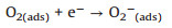
It has been well known that ZnO semiconductor for detection of reductive gases is based on the sensing effect of changing resistance. In details, ambient oxygen is adsorbed to the ZnO surface to generate an electron depletion layer. Subsequently, the resistance of ZnO is increased due to the loss of free electrons, and the oxygen that receives electrons is transformed into species O2-, O- and O2-. When the reductive gas of H2S is introduced into ZnO, it will react with the oxygen species. The reaction will cause decrease of the resistance since the lost free electrons will move back to the ZnO. When the H2S gas is removed from the air atmosphere, the oxygen will adsorb to the ZnO surface again to trap electrons from the ZnO, causing the resistance of the ZnO rise again. The general formula can be concluded as:
|
(2) |

|
(3) |
Now with the ZnO-ZnS heterojunction taken into consideration, a H2S sensing mechanism is proposed. As is illustrated in the schematic of Fig. 7, ZnS is a sensitive semiconductor material with the band gap (3.7 eV) wider than ZnO (3.32 eV). While ZnO is modified with ZnS to from ZnO-ZnS heterojunction, the redesigned band gap (2.4 eV) formed at the ZnO-ZnS interface region is narrower than that of either ZnO or ZnS, resulting in much lowered electron transfer resistance and faster electron transfer rate. Therefore, adsorbed oxygen is more likely to get electrons from ZnO to enhance the oxygen ion concentration on the surface of NWs. In the meanwhile, H2S reacts with more oxygen ions to emit more electrons to ZnO, leading to greater resistance reduction and larger response signal. However, when the ZnS film is too thick, the ZnO surface is completely covered by the ZnS shell. The thick ZnS shell, with a wide band gap, will greatly improve electron transfer resistance. It not only reduces the number of surfaces O2- but also increases the difficulty of releasing electrons to ZnO, thereby causing poor sensitivity to H2S gas.

|
Download:
|
| Fig. 7. Energy band diagram of ZnO, ZnS and ZnO-ZnS heterojunction. | |
In summary, this paper reveals the improved sensitivity of ZnOZnS heterostructure to ppm level H2S gas at low working temperature. Compared with the conventional ZnO-NWs material, the ZnO-ZnS nano-heterostructure formed by modifying ZnS on ZnO-NWs can effectively improve the H2S gas sensitivity within a wide temperature range, especially at the lower temperature than 300 ℃. The ZnO-ZnS-10 sensor, with the best sensor performance among the ZnO-ZnS-x, has not only high sensitivity to 1-5 ppm H2S but also good repeatability, stability and selectivity at the low temperature of 150 ℃. It can be concluded that ZnO nanowires modified with ZnS is an effective way to decrease sensor operating temperature and reduce heating power. The sensing mechanism of the ZnO-ZnS nano-heterostructure is expected to be applied to more chemical sensors.
Declaration of competing interestThe authors declare that they have no known competing financial interests or personal relationships that could have appeared to influence the work reported in this paper.
AcknowledgmentsThe authors appreciate the support from National Key R&D Program of China (No. 2016YFA0200800), the National Natural Science Foundation of China (Nos. 61527818, 61834007, 61604165, 61571430, 61874130, 61674160) and Science and Technology Development Fund of Shanghai Institute of Technology.
Appendix A. Supplementary dataSupplementary material related to this article can befound, inthe online version, at doi:https://doi.org/10.1016/j.cclet.2019.11.024.
| [1] |
N.S. Ramgir, P.K. Sharma, N. Datta, et al., Sens. Actuator. B-Chem. 186 (2013) 718-726. DOI:10.1016/j.snb.2013.06.070 |
| [2] |
K. Módis, E.M. Bos, E. Calzia, et al., Br. J. Pharmacol. 171 (2014) 2123-2146. DOI:10.1111/bph.12368 |
| [3] |
Y.L. Tang, Z.J. Li, J.Y. Ma, et al., J. Hazard. Mater. 280 (2014) 127-133. DOI:10.1016/j.jhazmat.2014.08.001 |
| [4] |
S.Y. Wang, J.Y. Ma, Z.J. Li, et al., J. Hazard. Mater. 285 (2015) 368-374. DOI:10.1016/j.jhazmat.2014.12.014 |
| [5] |
Y. Li, D.L. Li, J.C. Liu, Chin. Chem. Lett. 26 (2015) 304-308. DOI:10.1016/j.cclet.2014.12.002 |
| [6] |
W. Tang, J. Wang, Q. Qiao, et al., J. Mater. Sci. 50 (2015) 2605-2615. DOI:10.1007/s10853-015-8836-0 |
| [7] |
C.S. Rout, M. Hegde, C.N.R. Rao, Sens. Actuator. B-Chem. 128 (2008) 488-493. DOI:10.1016/j.snb.2007.07.013 |
| [8] |
Q. Zhang, H. Zhang, M.K. Xu, Z.R. Shen, Q. Wei, Chin. Chem. Lett. 29 (2018) 538-542. DOI:10.1016/j.cclet.2017.09.018 |
| [9] |
C.Y. Wang, Y.H. Li, P.P. Qiu, et al., Chin. Chem. Lett. 31 (2020) 1119-1123. DOI:10.1016/j.cclet.2019.08.042 |
| [10] |
W.C. Wang, F.Q. Liu, B. Wang, Y.D. Wang, Chin. Chem. Lett. 30 (2019) 1261-1265. DOI:10.1016/j.cclet.2018.12.030 |
| [11] |
Q. Geng, B. Karkyngul, C. Sun, et al., J. Mater. Sci. 52 (2017) 5097-5105. DOI:10.1007/s10853-017-0747-9 |
| [12] |
J. Huang, Q. Wan, Sensors 9 (2009) 9903-9924. DOI:10.3390/s91209903 |
| [13] |
J. Kim, W. Kim, K. Yong, J. Phys. Chem. C 116 (2012) 15682-15691. DOI:10.1021/jp302129j |
| [14] |
S. Ghosh, D. Adak, R. Bhattacharyya, et al., ACS Sens. 2 (2017) 1831-1838. DOI:10.1021/acssensors.7b00636 |
| [15] |
W. Zang, Y. Nie, D. Zhu, et al., J. Phys. Chem. C 118 (2014) 9209-9216. |
| [16] |
H.Y. Huang, P.C. Xu, D. Zheng, et al., J. Mater. Chem. A: Mater. Energy Sustain. 3 (2015) 6330-6339. DOI:10.1039/C4TA05963H |
| [17] |
Y.T. Han, Y. Liu, C. Su, et al., Sens. Actuator. B-Chem. 296 (2019) 126666. DOI:10.1016/j.snb.2019.126666 |
| [18] |
Y.T. Han, D. Huang, Y.J. Ma, et al., ACS Appl. Mater. Interfaces 10 (2018) 22640-22649. DOI:10.1021/acsami.8b05811 |
| [19] |
Y. Chen, P.C. Xu, X.X. Li, Y. Ren, Y.H. Deng, Sens. Actuator. B-Chem. 267 (2018) 83-92. DOI:10.1016/j.snb.2018.03.180 |