 2020, Vol. 31


b State Key Laboratory of Luminescent Materials and Devices, School of Materials Science and Engineering, South China University of Technology, Guangzhou 510640, China
Clean energy generation and saving play two equally important aspects for technique innovation, in order to maintain the sustainability of human societies. Semitransparent organic solar cells (ST-OSCs) became attractive to this end, due to their energy generation along with unique features [1-3], such as adjustable color, visible transparency, light-weight and flexibility, which enable OSCs with new field of application that differs from conventional inorganic ones [4-7]. Past efforts are mainly made to improve the energy generation and see-through functions of STOSC [8-14]. For instance, to tailor organic semiconductors with narrow gap yields near-infrared (NIR) absorbers with strong response to NIR solar photons, whereas exhibiting visible transparency [15-22].
Besides of energy generation, energy saving technique, such as passive radiative cooling, is also strongly needed to improve building energy efficiencies, hence mitigating energy spent on cooling of building [23]. These factors have promoted new design efforts to endow ST-OSCs with energy saving functionalities, i.e., heat insulation [24]. The success of this requires ST-OSCs possess visible light transmittance, whereas exhibiting strong absorption and/or reflection for low energy NIR and IR photons, which are prone to heat generation if not being utilized for photon-toelectron conversion, i.e., in wavelength of 780–2500 nm (approximately 53% of solar spectra). Distributed Bragg reflector (DBR) allows modulating the reflectance and transmission of incident light, which consists of an alternative stacking of transparent dielectric layers with large contrast of refractive indexes [25-34]. Nevertheless, to modulate the specific range of incident light requires the fine design of device layout and layer thickness. In addition, other challenges remain to develop efficient ST-OSC with multi-functionalities, requiring the delicate balance among key parameters, such as power conversion efficiency (PCE), average visible transmittance (AVT) and IR photon rejection rate (IRR) within one device. There present complicate trade-off and unclear structure-property relationships among materials, device architecture and performance parameters of ST-OSCs.
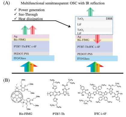
Therefore, to explore and exemplify the design guidance of multifunctional ST-OSCs, it would be beneficial to embed excellent optoelectronic performance and window functions into OSCs. Herein, we demonstrate new access to multifunctional ST-OSCs possessing excellent performance parameters, with high AVT near 30% and PCE of 7.3%, along with excellent IRR of over 93%, representing one of best multifunctional photovoltaics with power generation, see-through and heat dissipation functions in one device. They are the outcomes of integrative design efforts combining NIR absorbers, conductive interlayer, ultrathin metal film transparent electrode and DBR layers. Near-infrared absorbers with good visible transparency are chosen as the active layer. With the assistance of optical simulation, we have carefully adjusted device layout and designed new DBR with alternative stacking of tellurium oxide (TeO2) and lithium fluoride (LiF) films for the completion of ST-OSC. As a consequence, multifunctional ST-OSCs with DBR design can significantly outperform over the devices without DBR (24.5% AVT and 90.0% IRR). Besides, the optical properties of ST-OSCs are also much better than those of commercial heat-insulation films. Overall, this work demonstrates the integrative design approach to enable organic solar cells with practical perspectives for power-generating and heat-control window application.
ST-OSCs in this study are constructed in the conventional architecture of indium tin oxide (ITO)/PEDOT:PSS/PTB7-Th:IFIC-i-4 F/Bis-FIMG/ Ultrathin Silver (UT Ag), as shown in Fig. 1A and DBR layer is fabricated through alternative deposition of transparent dielectric layers with large contrast of refractive indexes of approximately 2.2 (TeO2) and 1.4 (LiF), respectively. The molecular structures of the conductive electron transporting material (BisFIMG), polymeric electron donor (PTB7-Th) and NIR acceptor (IFIC-i- 4 F), are presented in Fig. 1B. Note that PTB7-Th:IFIC-i-4 F active layer exhibits relatively weak visible absorption and strongNIR absorption up to 970 nm (Fig. S1 in Supporting information) [35]. Fullerene surfactant, bis-FIMG, is chosen as the electron transporting layer (ETL), owing to the excellent work function tuning toward electrode and suitable conductivity, low light absorption, as well as good film formation properties [36, 37]. In addition, it has previously demonstrated that the high quality UT Ag film can be achieved atop of fullerene surfactant as a seeding layer, which is to ensure good charge collection and light transmittance of transparent UT Ag electrodes.

|
Download:
|
| Fig. 1. (A) Schematic device architecture of conventional semi-transparent organic solar cell (ST-OSC), and multifunctional ST-OSC with distributed Bragg reflector (DBR). (B) The chemical structure of electron transport material (Bis-FIMG), polymer donor (PTB7-Th) and NIR acceptor (IFIC-i-4 F) employed in this study. | |
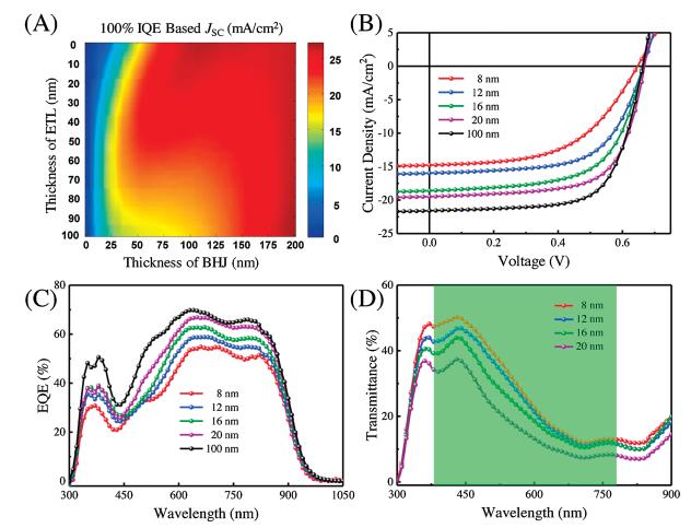
Prior to device fabrication, we performed optical simulation with transfer matrix model to probe the optimal layer thickness for ST-OSCs (Fig. 2A) [2]. The experimental results of fabricated devices are presented in Table S1 (Supporting information), revealing good PCEs can be achieved for active layer thickness around 88 nm with the different ETL thickness (8 nm, 12 nm and 16 nm). The conductive fullerene ETL exhibits merits that layer thickness is insensitive to the attainable device photocurrent. Therefore, in the case where the PCE is not much different, we finally choose the active layer of 88 nm and the ETL of 12 nm for construction of ST-OSCs, and vary the thickness of top ultrathin Ag electrode from 8 nm to 20 nm at an equal interval of 4 nm, to reach the balance between PCE and AVT of ST-OSCs. The device characteristics are presented in Figs. 2B–D and Table S2 (Supporting information), including current density-voltage (J-V) curves, external quantum efficiency (EQE) and transmittance spectra, respectively.

|
Download:
|
| Fig. 2. (A) Simulated JSC (IQE = 100%) in ST-OSCs as a function of active layer and electron transport layer thickness. (B) J-V characteristics, (C) external quantum efficiency (EQE) spectra and (D) transmittance spectra of ST-OSC devices with different silver thicknesses (green bar represents the visible range of the transmission spectrum). | |
It shows that device short-circuit current density (JSC) values are gradually improved, whereas the device AVT are decreased, with the increase of Ag thickness from 8 nm to 100 nm. AVT is calculated by the method of weighting the integration of the transmission spectrum (380–780 nm) against the photopic response of the human eye, as showing in below equation, which is generally accepted by the window industry [38].
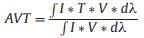
|
Where I is the spectrum of illuminant, T is the transmittance spectrum of device, V is the photopic spectral response of the human eye, and λ is the wavelength ranging from 380 nm to 780 nm [2]. The main reason is that Ag layer as light reflector can enhance the absorption of active layer, so that devices with thicker Ag perform higher photocurrent and lower AVT. For example, one typical opaque device (100 nm of thick silver) can yield high JSC of 21.6 mA/cm2 (calculated JSC of 20.11 mA/cm2 from the integration of EQE spectrum) and PCE of 9.6%, with open circuit voltage (VOC) of 0.66 V, and fill factor (FF) of 0.67. On the other hand, ST-OSCs with 8 nm ultrathin silver yield low PCEs of 5.1%, which could be ascribed to reduced conductivity and inferior charge collection of ultrathin silver. The fine balance of PCE and AVT can be achieved for ST-OSCs with 16 nm Ag, 88 nm active layer and 12 nm ETL layer, exhibiting 7.6% PCE and 24.5% AVT, with VOC of 0.66 V, JSC of 18.6 mA/cm2, and FF of 0.62.
The optical properties of ST-OSCs, such as transparency color perception, corresponding color temperature (CCT) and color rendering index (CRI) are presented in Table S3 (Supporting information), which are important criterion for the evaluation of suitability in window application [3]. The see-through photos of ST-OSCs are presented in Fig. S2 (Supporting information, taken under the same photographic settings), illustrating these ST-OSCs not only have excellent visible transparency, but also possess function as aesthetic color decoration for building integration.
For solar window in building integration, it would be ideal to pass visible photons for see-through function, and absorb NIR photons for power generation, while rejecting low energy NIR/IR photons (below the optical bandgap of absorber) for heat dissipation to save energy for buildings. Therefore, besides the AVT and PCE parameters of ST-OSCs, we further introduced a new design of DBR layer atop of Ag electrode to increase low energy NIR and IR photon rejection rate for above studied ST-OSCs. Considering the absorption band edge of the active layer, the design of the DBR layer is mainly to reflect photons with wavelength above 970 nm. We selected low refractive index LiF (1.4) and high refractive index TeO2 (2.2) to construct alternative multilayer DBR, and both transparent dielectric layers can be feasibly fabricated through deposition. With the assistance of optical simulations, the detail thickness values of the DBR layer from bottom to top are 10 nm LiF, 20 nm TeO2, 120 nm LiF and 100 nm TeO2, respectively.
The optical model is based on the wave optics and can numerically analyze the light propagation in thin film stacks [39]. Therefore, the functional relation between optical properties and layer thicknesses can be revealed through such an optical analysis. In this work, the reason for choosing two pairs of LiF/TeO2 DBR overlay layers is due to these two transparent dielectrics have large contrast of refractive indexes, and hence a strong interfacial coherence effect. On the other hand, itis relatively simple to fabricate two pairs of alternative stacks of DBR layers, whereas still remaining in effective to modulate NIR light. We have simulated over many different device architectures through the permutations of the thicknesses of the optically important layers, including BHJ, ultrathin Ag electrode and DBR structure. The absorption of the BHJ layer and the transmittance of the whole device were simulated, and the derived PCE, AVT, and IRR were achieved for each simulated device. The overall sorting of data maximizes the value of PCE, and then comprehensively considers AVT and IRR values to obtain an optimal equilibrium value for experimental screening.
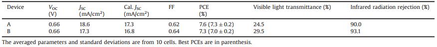
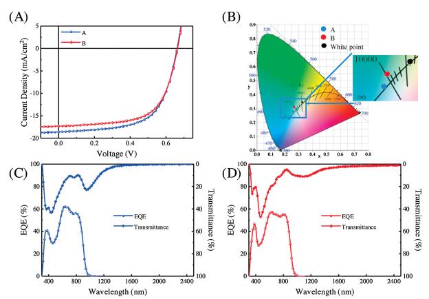
The photovoltaic performance and optical properties of ST-OSCs were compared between devices without DBR (device A) and with DBR (device B), as shown in Table 1 and Figs. 3A–D. The optimal devices were employed TeO2/LiF DBR layers atop of 16 nm ultrathin Ag electrode, showing the enhancement of both NIR photon rejection and visible transmittance (Fig. 3D), which is due to the DBR layer shift the transmittance spectra in the visible range. Note that device with DBR design has a significant improvement of device AVT from 24.5% (without DBR) to 29.5% (with DBR), along with the enhanced IRR of over 93% without sacrificing the PCE of ST-OSCs. The improvement of AVT is mainly because the engineering of DBR leads to the red shift of main transmittance peak in the visible light region from 420 nm to 500 nm (Fig. 3D), which is in good agreement with the trend of photopic response curve in AVT calculation formula. The device with DBR layer exhibits CIE coordinates of (0.269, 0.319) when comparing to the devices without DBR (0.262, 0.289), which is closer to the white point (0.33, 0.33) (Fig. 3B). The photovoltaic performance of STOSCs showed the negligible change (remaining ~7%) after the introduction of DBR atop of the Ag electrode. The J–V curve and EQE spectra are shown in Figs. 3A, C and D, respectively.
|
|
Table 1 Photovoltaic parameters and optical parameters of ST-OSCs without (A) or with (B) distributed Bragg reflectors. |

|
Download:
|
| Fig. 3. (A) The J-V characteristics, (B) Color coordinates, Transmittance spectra and external quantum efficiency (EQE) spectra of ST-OSCs without (device A) (C) and with (device B) DBR layers (D), respectively. | |
Besides device AVT showing significant improvement, photovoltaic parameters of device (with DBR) such as VOC, JSC and FF are almost identical to device (without DBR). Note that the IR rejection rate has over 9% enhancement at the range of 970–1100 nm. And the overall IRR reaches over 93% for device B (with DBR) (calculated from the overall range of 780–2500 nm). These properties are superior to those devices without DBR layers, and much better than those of commercial heat-insulation films, like 3 M P-18ARL (AVT is 15.9% and the IR rejection rate is 90.9%) [24]. With these results in hand, we have demonstrated herein that the new design of ST-OSCs can lead to effective low energy IR photon rejection and remain overall good AVT and PCE values, which would be promising for the use as power-generating and heat-control windows for building integration.
In summary, we have designed and fabricated multifunctional semitransparent organic solar cells with the potential application of power-generating and heat-control windows for building integration.These proto-typeST-OSCshave shown state-of-art performance parameters with near 30% AVT and PCE of 7.3%, as well as an outstanding IR rejection rate of over 93% in the range of 780– 2500 nm. It demonstrates that multifunctional ST-OSCs with a fine balance of PCE, AVT and IRR can be achieved from the careful tuning of or ganic materials, transparent electrode and DBR layer. In addition to the absorption spectra of the active layer, the improvement of visible transmittance and infrared reflection can be further achieved from the precise design of the device layout and DBR layer. Overall, we have demonstrated that multifunctional ST-OSC devices possessing excellent performance parameters, such PCE, AVT and IRR, would be promising for power window application with energy generation, see-through and heat dissipation functions.
AcknowledgmentsThis research was funded by Ministry of Science and Technology (No. 2017YFA0206600), National Natural Science Foundation of China (Nos. 21722404, 21674093, 21734008, 21761132001 and 91633301), International Science and Technology Cooperation Program of China (ISTCP, No. 2016YFE0102900) and supported by the Fundamental Research Funds for the Central Universities (No. 2018XZZX002-16). C.-Z. Li thanks the support by Zhejiang Natural Science Fund for Distinguished Young Scholars (No. LR17E030001).
Appendix A. Supplementary dataSupplementarymaterial related to this article can befound, in the online version, at doi:https://doi.org/10.1016/j.cclet.2019.08.046.
| [1] |
Q. Xue, R. Xia, C.J. Brabec, H.L. Yip, Energy Environ. Sci. 11 (2018) 1688-1709. DOI:10.1039/C8EE00154E |
| [2] |
R. Xia, C.J. Brabec, H.L. Yip, Y. Cao, Joule 3 (2019) 2241-2254. DOI:10.1016/j.joule.2019.06.016 |
| [3] |
J. Zhang, G. Xu, F. Tao, et al., Adv. Mater. 31 (2019) e1807159. DOI:10.1002/adma.201807159 |
| [4] |
Y. Liu, P. Cheng, T. Li, et al., ACS Nano 13 (2019) 1071-1077. DOI:10.1021/acsnano.8b08577 |
| [5] |
H. Shi, R. Xia, G. Zhang, et al., Adv. Energy Mater. 9 (2019) 1803438. DOI:10.1002/aenm.201803438 |
| [6] |
D. Landerer, D. Bahro, H. Rçhm, et al., Energy Technol. 5 (2017) 1936-1945. DOI:10.1002/ente.201700226 |
| [7] |
H. Kim, H.S. Kim, J. Ha, et al., Adv. Energy Mater. 6 (2016) 1502466. DOI:10.1002/aenm.201502466 |
| [8] |
W. Yu, L. Shen, P. Shen, et al., ACS Appl. Mater. Interfaces 6 (2014) 599-605. DOI:10.1021/am405274z |
| [9] |
J.Y. Lee, K.T. Lee, S. Seo, L.J Guo, Sci. Rep. 4 (2014) 4192. |
| [10] |
C.Y. Chang, L. Zuo, H.L. Yip, et al., Adv. Energy Mater. 4 (2014) 1301645. DOI:10.1002/aenm.201301645 |
| [11] |
W. Yu, L. Shen, P. Shen, et al., Sol. Energy Mater. Sol. Cells 117 (2013) 198-202. DOI:10.1016/j.solmat.2013.06.002 |
| [12] |
R. Betancur, P. Romero-Gomez, A. Martinez-Otero, et al., Nat. Photonics 7 (2013) 995-1000. DOI:10.1038/nphoton.2013.276 |
| [13] |
Z. Tang, Z. George, Z. Ma, et al., Adv. Energy Mater. 2 (2012) 1467-1476. DOI:10.1002/aenm.201200204 |
| [14] |
K.S. Chen, J.F. Salinas, H.L. Yip, et al., Energy Environ. Sci. 5 (2012) 9551-9557. DOI:10.1039/c2ee22623e |
| [15] |
Z. Xiao, X. Jia, L. Ding, Sci. Bull. 62 (2017) 1562-1564. DOI:10.1016/j.scib.2017.11.003 |
| [16] |
L. Liu, Q. Liu, Z. Xiao, et al., Sci. Bull. 64 (2019) 1083-1086. DOI:10.1016/j.scib.2019.06.005 |
| [17] |
L. Meng, Y. Zhang, X. Wan, et al., Science 361 (2018) 1094-1098. DOI:10.1126/science.aat2612 |
| [18] |
Y. Cui, C. Yang, H. Yao, et al., Adv. Mater. 29 (2017) 1703080. DOI:10.1002/adma.201703080 |
| [19] |
F. Ullah, S. Qian, W. Yang, et al., Chin. Chem. Lett. 28 (2017) 2223-2226. DOI:10.1016/j.cclet.2017.08.009 |
| [20] |
J.Q. Xu, W. Liu, S.Y. Liu, et al., Sci. China Chem. 60 (2017) 561-569. DOI:10.1007/s11426-016-9003-9 |
| [21] |
B. Wang, W. Liu, H. Li, et al., J. Mater. Chem. A 5 (2017) 9396-9401. DOI:10.1039/C7TA02582C |
| [22] |
Z. Zhang, W. Liu, T. Rehman, et al., J. Mater. Chem. A 5 (2017) 9649-9654. DOI:10.1039/C7TA01554B |
| [23] |
T. Li, Y. Zhai, S. He, et al., Science 364 (2019) 760-763. DOI:10.1126/science.aau9101 |
| [24] |
C. Sun, R. Xia, H. Shi, et al., Joule 2 (2018) 1816-1826. DOI:10.1016/j.joule.2018.06.006 |
| [25] |
P. Shen, G. Wang, B. Kang, et al., ACS Appl. Mater. Interfaces 10 (2018) 6513-6520. DOI:10.1021/acsami.7b18765 |
| [26] |
J.H. Lu, Y.H. Lin, B.H. Jiang, et al., Adv. Funct. Mater. 28 (2018) 1703398. DOI:10.1002/adfm.201703398 |
| [27] |
Y. Kim, J. Son, S. Shafian, et al., Adv. Opt. Mater. 6 (2018) 1800051. DOI:10.1002/adom.201800051 |
| [28] |
S.Y. Chang, P. Cheng, G. Li, Y. Yang, Joule 2 (2018) 1039-1054. DOI:10.1016/j.joule.2018.04.005 |
| [29] |
G. Xu, L. Shen, C. Cui, et al., Adv. Funct. Mater. 27 (2017) 1605908. DOI:10.1002/adfm.201605908 |
| [30] |
Q. Liu, P. Romero-Gomez, P. Mantilla-Perez, et al., Adv. Energy Mater. 7 (2017) 1700356. DOI:10.1002/aenm.201700356 |
| [31] |
W. Yu, L. Shen, X. Jia, et al., RSC Adv. 5 (2015) 54638-54644. DOI:10.1039/C5RA08137H |
| [32] |
F. Pastorelli, P. Romero-Gomez, R. Betancur, et al., Adv. Energy Mater. 5 (2015) 1400614. DOI:10.1002/aenm.201400614 |
| [33] |
J. Huang, C.Z. Li, C.C. Chueh, et al., Adv. Energy Mater. 5 (2015) 1500406. DOI:10.1002/aenm.201500406 |
| [34] |
L. Shen, S. Ruan, W. Guo, et al., Sol. Energy Mater. Sol. Cells 97 (2012) 59-63. DOI:10.1016/j.solmat.2011.09.004 |
| [35] |
F.X. Chen, J.Q. Xu, Z.X. Liu, et al., Adv. Mater. 30 (2018) e1803769. DOI:10.1002/adma.201803769 |
| [36] |
K. Yan, Z.X. Liu, X. Li, et al., Org. Chem. Front. 5 (2018) 2845-2851. DOI:10.1039/C8QO00788H |
| [37] |
K. Yan, C.Z Li, Macromol. Chem. Phys. 220 (2019) 1900084. DOI:10.1002/macp.201900084 |
| [38] |
C.J. Traverse, R. Pandey, M.C. Barr, R.R. Lunt, Nat. Energy 2 (2017) 849-860. DOI:10.1038/s41560-017-0016-9 |
| [39] |
R. Xia, H. Gu, S. Liu, et al., Sol. RRL 3 (2019) 1800270. DOI:10.1002/solr.201800270 |