 2020, Vol. 31


Electromagnetic interference (EMI) shielding materials arise a lot of interests due to they are efficient shielding against electromagnetic (EM) wave radiation pollution [1-3]. It is known that the high electrical conductivity is critical for the EMI shielding materials [4]. Metals are conventionally used as shielding materials. However, the requirement for lighter and thinner EMI shielding materials is more and more urgent, which means that metal is not suitable for the practical application because they are heavy [5]. To solve this problem, a lot of carbon-based materials such as carbon black, carbon spheres, carbon nanotubes (CNTs) and graphenes, are developed due to their low density and high conductivity [6-9]. Considering flexibility, graphenes are more suitable as two-dimensional (2D) materials. However, the high cost and difficulty to prepare graphenes with large scale restrain the practical application [10]. MXenes, as a new family of 2D materials, have drawn a lot of attention due to their unique 2D structure. Among them, Ti3C2Tx, as the first discovered MXenes, stands out to be efficient EMI shielding materials, where Tx represents the surface functional groups [11-13]. Compared with graphenes, Ti3C2Tx MXenes are easier to prepare with low cost and large scale [14]. The electrical conductivity of Ti3C2Tx can be as high as 6400 S/cm [15], revealing the great potentianl as EMI shielding materials. Shahzad et al. prepared Ti3C2Tx films through a vacuum assisted filtration (VAF) method [11]. When the thickness is only 45 μm, the EMI shielding effectiveness can reach as high as 90 dB. A lot of Ti3C2Tx-based EMI shielding materials also have been prepared, such as Ti3C2Tx/CNTs [5], Ti3C2Tx/graphene [16] and Ti3C2Tx/PVA [17].
The EMI shielding mechanisms mainly contain EM wave reflection on the surface and EM wave absorption in materials. To avoid undesirable emissions of EM wave on the surface of EMI shielding materials, it is important to enhance the absorption and weaken the reflection [1, 18].
Liu et al. prepared Ti3C2Tx foams by hydrazine reduction [19]. The porous structure leads to higher absorption than bulk film. Xu et al. prepared Ti2CTx/PVA foams through the freeze-drying method [18]. The reflection effectiveness is less than 2 dB, revealing the absorption-dominated shielding mechanism. According to these results, it can be concluded that the key to increase the absorption of the EMI shielding materials is the formation of porous structure and the introduction of low conductive phase to enhance the scattering.
Carbon black (CB), as one of the most commonly used carbon materials, has drawn a lot of attention due to the large surface area, adjustable diameter and low cost. The dispersion of CB particles in Ti3C2Tx film can lead to the porous structure, increasing the surface areas. Moreover, the electrical conductivity of CB is lower than Ti3C2Tx, preventing the stronger surface reflection. So, it is expected to enhance EM absorption by the combination of CB and Ti3C2Tx.
Herein, we demonstrate the fabrication of freestanding and flexible Ti3C2Tx-bonded CB films by the VAF method. The incorporation of the CB particles can lead to porous structure in the film, enhancing the scattering of the EM wave, which can increase the absorption of the EM wave.
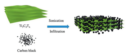
The preparation process of Ti3C2Tx-bonded CB films is shown in Fig. 1. The Ti3C2Tx is prepared through in-situ HF etching. The LiFHCl etchant is employed to etch the Al atoms [20]. Then, hand shaking and centrifugation methods are used for delamination. The final product is Ti3C2Tx suspension of 2 mg/mL. According to Fig. S1 (Supporting information), the diameter of Ti3C2Tx is about 500 nm and the thickness is very small. The high-magnification morphology of Ti3C2Tx flakes is shown in Fig. S1b. The lattice fringes are clear and the insert SAED patterns show the hexagonal crystal structure of Ti3C2Tx. Then, CB particles were added to 20 mL of the above suspension followed by sonication of 30 min. The microstructure of CB particles is shown in Fig. S2 (Supporting information). The CB particles have a uniform diameter of about 10 nm. The mixed dispersions were vacuum filtered by polyvinylidene difluoride (PVDF) membranes and then vacuum dried at 80 ℃ for 6 h to obtain freestanding and flexible films. The amount of CB particles added into the Ti3C2Tx suspensions are 0, 10, 30, 50, 70 and 90 mg, respectively, which are denoted as samples M0, M1, M2, M3, M4 and M5.

|
Download:
|
| Fig. 1. Schematic diagram for the fabrication of Ti3C2Tx-bonded CB films. | |
The macroscopic image of the prepared Ti3C2Tx-bonded CB film is shown in Fig. 2a. It can be seen that the film is freestanding and flexible. The thickness of Ti3C2Tx-bonded CB films can be seen from Fig. S3 (Supporting information). The thickness of these films varies with the increase of CB particles content, which means that the CB particles are intercalated into the layer of Ti3C2Tx. Due to the low density of CB particles, the thickness of films increases significantly from 20 mm to 64 mm. The cross-sectional SEM images of Ti3C2Tx-bonded CB films are shown in Figs. 2b-g. The high-magnification SEM images of Ti3C2Tx film show that the structure is compact and thus the thickness is also small, which will cause strong reflection of the EM wave. After mixed with CB particles, the layer structure becomes loose and the particles are dispersed randomly among the flakes of Ti3C2Tx. Furthermore, with the increase of the CB particles content, there are a lot of pores generated in the films, especially in Figs. 2f and g. As can be seen in Fig. 2g, the parallel layer structure of Ti3C2Tx-bonded CB film has been interrupted due to the excessive amount of CB particles. Also, when the content of CB particles increases to 110 mg, it is impossible to form a film (Fig. S4 in Supporting information). According to the EDS mapping of Ti (Fig. 2h), it can be seen that the Ti3C2Tx disperses well in the whole film.

|
Download:
|
| Fig. 2. Macroscopic image of Ti3C2Tx-bonded CB films (a); high-magnification SEM images of Ti3C2Tx-bonded CB films of samples M0 (b), M1 (c), M2 (d), M3 (e), M4 (f), M5 (g) and corresponding EDS mapping of Ti (h). | |
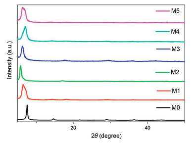
According to the XRD pattern in Fig. 3, the (002) peak of the pure Ti3C2Tx film located at 2θ = 7.54°, which is in agreement with the layer structure of the Ti3C2Tx. It is obvious that the (002) peak of the Ti3C2Tx becomes broader and shifts to smaller angels after mixed with CB particles. These results indicate that the orderly arrangement between Ti3C2Tx layers is interrupted and CB particles enlarge the space between Ti3C2Tx flakes, which can enhance absorption through scattering [21, 22]. Due to the high diffraction intensity of Ti3C2Tx, the peak of CB is invisible.

|
Download:
|
| Fig. 3. XRD patterns of Ti3C2Tx-bonded CB films with different CB loadings. | |
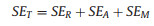
The EMI shielding performances of the Ti3C2Tx-bonded CB films at X band are shown in Fig. 4. Generally, the total EMI shielding effictiveness (SET) mainly contains EM wave reflection on the surface of materials, EM wave absorption in materials and multiple reflection, which are denoted as SER, SEA and SEM. The relationship of them is as follows (Eq. 1) [23, 24]:
|
(1) |

|
Download:
|
| Fig. 4. EMI SE values of Ti3C2Tx-bonded CB films (a) and SET, SER, SEA values of them (b). Reflection (c), absorption (d) and transmission (e) and coefficients of Ti3C2Tx-bonded CB films. | |
The multiple reflections can be neglected when the SET is larger than 15 dB. Fig. 4a exhibits the EMI SE as a function of frequency for all the films. When the contents of CB particles are lower than 50 mg, the EMI SE are almost the same. With higher contents of CB particles, the EMI SE slightly increases. Sample M4 possesses the highest EMI SE. The calculated specific SE can be as high as 8718 dB cm2/g, indicating excellent EMI shielding performance. The detailed information of EMI SE values including SET, SER and SEA are shown in Fig. 4b. It can be seen that the SET values of all six films are higher than 50 dB, which means that more than 99.999% of the EM energy can be shielded, revealing excellent EMI shielding performance. Also, it is believed that these films can show similar performance in the whole 2-18 GHz. This can be attributed to the high electrical conductivity of Ti3C2Tx. For all the films, the values of SEA are higher than SER. However, it is noted that the ratios of SER and SEA are different. Generally, higher SEA values are better. With the increase of the CB particles content, the values of SER decrease slightly, which can be attributed to the looser structures of the Ti3C2Tx layers. It is obvious that the SEA value gradually increases and SER value gradually decreases with the increase of the CB particles content. It can be found that when the content of CB particles is 70 mg, the SET is highest. When the content of CB particles is 90 mg, the SET value decreases slightly due to the significant decrease of SER, which can be attributed to the interrupted parallel structure of the film. To further explore EMI shielding mechanisms, the reflection (R), absorption (A) and transmission (T) coefficients of all the six films are calculated based on the measured S parameters (Eqs. 2–4) [25]:

|
(2) |

|
(3) |

|
(4) |
It can be seen that with the increase of the CB particles content, the R and T show the opposite trend. The R decrease and the A increase, which means that the reflection of the wave is weakened and the absorption is enhanced. The T decreases continuously at first, revealing better shielding performance with the increase of the CB particles content. However, when the content of CB particles is 90 mg, the T slightly increases. It can be concluded that although the higher content of CB particles can lead to high absorption inner materials through scattering, the reflection decreases significantly due to the interrupted parallel structure, causing low conductivity.
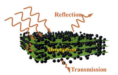
The EMI shielding mechanisms are summarized in Fig. 5. The high electrical conductivity of the Ti3C2Tx is the foundation for the efficient EMI shielding. After mixed with CB particles, the layer structure of Ti3C2Tx becomes loose and some pores are generated. These facilitate the absorption of the EM wave through enhancing the reflection and scattering at the interface of the layers and pores.

|
Download:
|
| Fig. 5. Schematic illustration of the interaction mechanism between EM wave and Ti3C2Tx-bonded CB films. | |
In conclusion, the Ti3C2Tx-bonded CB films with enhanced EM wave absorption performance are prepared. The Ti3C2Tx prepared with LiF-HCl etchant possesses high electrical conductivity, which increase of the CB particles content, porous structure can be formed in the films, which can enhance scattering and reflection causing by the porous structure, leading to the increase of the absorption attenuation and the decrease of the reflection. It is notable that the SET keeps increasing during this process. The SER decreased from 20 dB to 12 dB and the SEA increased from 31 dB to 47 dB. The best EMI shielding effectiveness can be as high as 60 dB.
Declaration of competing interestThe authors declare that they have no known competing financial interests or personal relationships that could have appeared to influence the work reported in this paper.
AcknowledgmentsThis work was financially supported by the National Science Fund for Distinguished Young Scholars (No. 51725205), the National Natural Science Foundation of China (No. 51821091). The authors would like to give their special thanks to Prof. Xiaowei Yin for his kind guidance and help on the research work.
Appendix A. Supplementary dataSupplementary material related tothis article canbefound, in the online version, at doi:https://doi.org/10.1016/j.cclet.2020.01.030.
| [1] |
B. Zhao, C. Zhao, R. Li, S.M. Hamidinejad, C.B. Park, ACS Appl. Mater. Interfaces 9 (2017) 20873-20884. DOI:10.1021/acsami.7b04935 |
| [2] |
Y. Zhang, W. Tian, L. Liu, et al., Chem. Eng. J. 372 (2019) 1077-1090. DOI:10.1016/j.cej.2019.05.012 |
| [3] |
X. Wang, J. Shu, W. Cao, et al., Chem. Eng. J. 369 (2019) 1068-1077. DOI:10.1016/j.cej.2019.03.164 |
| [4] |
M.S. Cao, Y.Z. Cai, P. He, et al., Chem. Eng. J. 359 (2019) 1265-1302. DOI:10.1016/j.cej.2018.11.051 |
| [5] |
G. Weng, J. Li, M. Alhabeb, et al., Adv. Funct. Mater. (2018) 1803360. |
| [6] |
L. Kong, X. Yin, H. Xu, et al., Carbon 145 (2019) 61-66. DOI:10.1016/j.carbon.2019.01.009 |
| [7] |
W. Cao, C. Ma, S. Tan, et al., Nano-Micro Lett. 11 (2019) 72. DOI:10.1007/s40820-019-0304-y |
| [8] |
S. Zhao, H.B. Zhang, J.Q. Luo, et al., ACS Nano 12 (2018) 11193-11202. DOI:10.1021/acsnano.8b05739 |
| [9] |
L. Jia, M. Li, D. Yan, et al., J. Mater. Chem. C 5 (2017) 8944-8951. DOI:10.1039/C7TC02259J |
| [10] |
B. Shen, W. Zhai, W. Zheng, Adv. Funct. Mater. 24 (2014) 4542-4548. DOI:10.1002/adfm.201400079 |
| [11] |
F. Shahzad, M. Alhabeb, C.B. Hatter, et al., Science 353 (2016) 1137-1140. DOI:10.1126/science.aag2421 |
| [12] |
M. Han, X. Yin, H. Wu, et al., ACS Appl. Mater. Interfaces 8 (2016) 21011-21019. DOI:10.1021/acsami.6b06455 |
| [13] |
W. Yuan, L. Cheng, Y. An, et al., ACS Sustain. Chem. Eng. 6 (2018) 8976-8982. DOI:10.1021/acssuschemeng.8b01348 |
| [14] |
M. Naguib, V.N. Mochalin, M.W. Barsoum, Y. Gogotsi, Adv. Mater. 26 (2014) 992-1005. DOI:10.1002/adma.201304138 |
| [15] |
C. Couly, M. Alhabeb, K.L. Van Aken, et al., Adv. Electron. Mater. 4 (2018) 1700339. DOI:10.1002/aelm.201700339 |
| [16] |
Z. Fan, D. Wang, Y. Yuan, et al., Chem. Eng. J. 381 (2020) 122696. DOI:10.1016/j.cej.2019.122696 |
| [17] |
X. Jin, J. Wang, L. Dai, et al., Chem. Eng. J. 380 (2020) 122475. DOI:10.1016/j.cej.2019.122475 |
| [18] |
H. Xu, X. Yin, X. Li, et al., ACS Appl. Mater. Interfaces 11 (2019) 10198-10207. DOI:10.1021/acsami.8b21671 |
| [19] |
J. Liu, H.B. Zhang, R. Sun, et al., Adv. Mater. 29 (2017) 1702367. DOI:10.1002/adma.201702367 |
| [20] |
M. Alhabeb, K. Maleski, B. Anasori, et al., Chem. Mater. 29 (2017) 7633-7644. DOI:10.1021/acs.chemmater.7b02847 |
| [21] |
L. Yu, L. Hu, B. Anasori, et al., ACS Energy Lett. 3 (2018) 1597-1603. DOI:10.1021/acsenergylett.8b00718 |
| [22] |
X. Li, X. Yin, M. Han, et al., J. Mater. Chem. C 5 (2017) 4068-4074. DOI:10.1039/C6TC05226F |
| [23] |
X. Liu, X. Yin, L. Kong, et al., Carbon 68 (2014) 501-510. DOI:10.1016/j.carbon.2013.11.027 |
| [24] |
M. Chen, X. Yin, M. Li, et al., Ceram. Int. 41 (2015) 2467-2475. DOI:10.1016/j.ceramint.2014.10.062 |
| [25] |
X. Liu, Z. Yu, R. Ishikawa, et al., Acta Mater. 130 (2017) 83-93. DOI:10.1016/j.actamat.2017.03.031 |