 2020, Vol. 31


Lithium-ion batteries (LIBs) won the Nobel Prize in 2019, proving their great success after development of more than 20 years [1, 2]. Nevertheless, the energy density of the state-of-the-art LIBs is unable to keep pace with the development of electric vehicles due to the low specific capacity of commercial electrode materials. The theoretical specific capacity of commercial cathode materials is usually below 300 mAh/g. For anode materials, the commercial graphite only has a theoretical specific capacity of 372 mAh/g [3]. Accordingly, electrode materials with high specific capacity are urgently required [4-10]. Recently, silicon monoxide (SiO) as a promising anode material has captured widespread attention due to its high theoretical specific capacity (~2400 mAh/g), low working potential (< 0.5 V vs. Li+/Li), low cost, easy synthesis, nontoxicity and abundant natural source [11]. In addition, the irreversible products like Li2O and Li4SiO4 formed in the initial lithiation process of SiO can buffer the volume change during the following charge-discharge process, which makes SiO own smaller volume expansion and better cycling performance than Si [11]. However, several issues impede its practical application [12]. One is the inevitable volume expansion (~200%), which can result in cracks of the electrode and electrical isolation of active materials. The second one is the low intrinsic electrical conductivity, which compromises the electrochemical activity and rate capability. Another one is the low ICE originating from the irreversible reaction and the formation of solid electrolyte interphase (SEI) during the initial lithiation process. To address these issues, a serious of strategies have been proposed, such as fabricating SiO/C composite [13-16], optimizing synthesis process [17], using multifunctional conductive agent or binders [18, 19], designing nanostructures [20], oxide coating [21], metallic or heteroatom doping [22, 23], prelithiation engineering [24], modifying electrolyte [25] and utilizing special additives [26]. Although certain progress has been achieved, a comprehensive strategy taking into account all the issues of SiO still needs to be explored.
Just like graphene [27, 28], MXene is a two-dimensional (2D) material and has been successfully applied in various branches of energy storage [29, 30]. Ti3C2Tx (Tx represents surface terminations such as -OH, -O and -F groups) is the most widely studied MXene and it has superior electronic conductivity (4600±1100 S/cm), low Li+ diffusion barrier (0.07 eV) and flexible mechanical properties [31, 32]. The issues of Si have been alleviated with the help of Ti3C2Tx MXene [33, 34]. Inspired by the similar properties between Si and SiO, here we fabricated SiO-WM by an electrostatic selfassembly method. Importantly, this method is simple, scalable and taking into account all the issues of SiO. MXene can address the issues of SiO from the following three aspects: (1) The wrinkled 2D MXene nanosheets can tightly couple the SiO particles and avoid the electrical isolation of active materials resulting from volume expansion during the long cycling process; (2) MXene with high electronic conductivity can improve the issue of low intrinsic electrical conductivity of SiO; (3) The incorporation of MXene decreases the relative content of SiO in the composite, which can increase the ICE. As a result, when used as anode materials, the SiOWM exhibited improved rate capability, cycling performance and ICE compared with bare SiO.
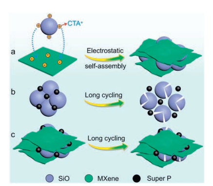
Stable Ti3C2Tx suspension was prepared by in-situ etching Ti3AlC2 powders using LiF and HCl according to previous report (Fig. S1a in Supporting information) [35]. The Ti3C2Tx suspension could be processed into a flexible film by a vacuum filtration method (Figs. S1b and c in Supporting information) [36]. Fig. 1a is the schematic showing the electrostatic self-assembly process of SiO-WM. The existence of terminations made the surface of Ti3C2Tx nanosheets negatively charged. The surface of SiO can be positively charged after decorated by Cetyltrimethylammonium bromide (CTAB) aqueous solution (Fig. S1d in Supporting information) [37]. When positively charged SiO particles were added into Ti3C2Tx suspension, electrostatic self-assembly between SiO particles and Ti3C2Tx nanosheets happened immediately (Fig. S1e in Supporting information). The stability of Ti3C2Tx suspension was destroyed and an aggregation phenomenon was detected (Fig. S1f in Supporting information). In addition, the flat Ti3C2Tx nanosheets became wrinkled due to the existence of CTAB, which could induce the crumpling of Ti3C2Tx nanosheets by destroying the balance (repulsion force) between Ti3C2Tx nanosheets through positive/negative charge neutralization [38, 39]. The SiO-WM was obtained after filtration and drying in vacuum. For bare SiO, pulverization and delamination caused by large volume expansion in the long cycling process can result in electrical isolation of active materials, finally leading to a severe capacity decay (Fig. 1b). While for SiOWM, 2D wrinkled MXene nanosheets with high electronic conductivity, large surface area and flexibility can relieve the volume expansion in the long cycling process and keep the electrical connection of the active materials, resulting in an improved cycling performance (Fig. 1c). Importantly, the wrinkled MXene nanosheets cannot impede the transport of Li+ due to its low Li+ diffusion barrier (0.07 eV).

|
Download:
|
| Fig. 1. (a) Schematic showing the electrostatic self-assembly process of SiO-WM. (b) Formation of electrical isolation in bare SiO electrode during the long cycling process caused by volume expansion and recovery. (c) Wrinkled MXene nanosheets with high electronic conductivity, large surface area and flexibility can keep the electrical connection of SiO active materials during the long cycling process. | |
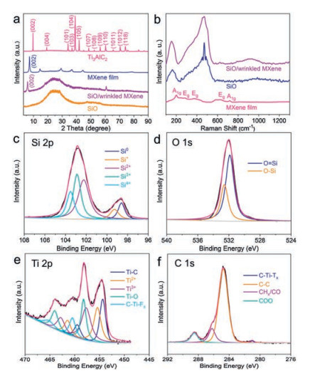
X-ray diffraction (XRD) was used to analyse the phase constitution of the samples (Fig. 2a). After etching Al layers from Ti3AlC2, the (104) peak at around 39° disappeared and the (002) peak was shifted to a smaller angle, indicating Ti3C2Tx was successfully synthesized [40]. The broad peak at around 25° indicated the amorphous state of the SiO [41]. After the electrostatic self-assembly process, the SiO-WM exhibited characteristic peaks of both Ti3C2Tx MXene and amorphous SiO. Compared with MXene film, an obvious peak at around 60° was observed in SiO-WM, because a fraction of the basal planes of MXene in the composite were not parallel to the underlying XRD sample holder, which was consistent with the randomly oriented multilayered Ti3C2 particles on the sample holder [38, 42]. The location of the (002) peak of SiO-WM shifted to a smaller angle compared with that of MXene film, which should attribute to the gradually increased lattice spacing of MXene expanded by SiO particles [43] or the intercalating of CTA+ cation into MXene [38].

|
Download:
|
| Fig. 2. (a) XRD patterns of the samples. (b) Raman spectra of the samples. (c–f) XPS spectra of Si 2p, O 1s, Ti 2p and C 1s in SiO-WM. | |
Raman was carried out to further probe the structural information of the samples (Fig. 2b). For MXene film, the modes located at around 198 and 717 cm-1 are attributed to A1g symmetry out-of-plane vibrations of Ti and C atoms, respectively. The modes located at around 280, 390 and 622 cm-1 are belonging to Eg group vibrations, including in-plane (shear) modes of Ti, C and the functional group atoms on the surface [31]. For SiO, two broad peaks centered at 161.5 and 472 cm-1 are ascribed to amorphous SiO [44]. The Raman spectrum of SiO-WM is the superposition of the spectra of SiO and MXene.
X-ray photoelectron spectroscopy (XPS) was conducted to investigate the chemical composition and surface state of the elements in SiO-WM. XPS full spectrum (Fig. S2 in Supporting information) indicated the existence of Si, O, Ti and C elements. The high-resolution spectra of Si 2p, O 1s, Ti 2p and C 1s were presented to further probe their chemical states. The Si 2p peak could be divided into five small peaks centered at 98.6, 99.3, 102.2, 102.9 and 103.5 eV, corresponding to Si°, Si+, Si2+, Si3+ and Si4+ species, respectively [16]. The binding energies of O 1s at 531.9 and 532.6 eV are belonging to Si=O and Si-O bonds, respectively [16]. The binding energies of Ti 2p centered at 454.4 (459.5), 455.4 (461.4), 457.7 (462.8), 458.2 (464.0) and 460.4 (465.2) eV are corresponding to Ti-C, Ti2+, Ti3+, Ti-O and C-Ti-Fx bonds, respectively [39]. The binding energies of C 1s centered at 281.0, 284.8, 286.2 and 288.5 eV are corresponding to C-Ti-Tx, C-C, CHx/CO and COO bonds, respectively [39].
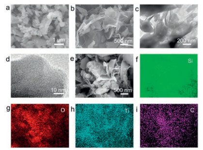
Scanning electron microscope (SEM) was performed to probe the microstructure of the samples. The particle size of SiO is not homogeneous (Fig. 3a and Fig. S3 in Supporting information). Ti3AlC2 particles are big bulks (Fig. S4a in Supporting information). After the electrostatic self-assembly process, SiO particles were encapsulated in wrinkled MXene nanosheets (Fig. 3b and Fig. S4b in Supporting information). Transmission electron microscopy (TEM) was employed to deeply observe the morphology of SiOWM. SiO particles are encapsulated by wrinkled MXene nanosheets (Fig. 3c). No obvious lattice fringes for SiO were found (Fig. 3d), indicating its amorphous state, which was consistent with the XRD results. EDS elemental mapping further verified the above results (Figs. 3e–i). This structure can relieve the volume change in the charge-discharge process and prevent the electrical isolation of active materials.

|
Download:
|
| Fig. 3. (a) SEM image of SiO particles. (b) SEM image of SiO-WM. (c) TEM image of SiO-WM. (d) TEM image of SiO in SiO-WM. (e–i) SEM image of SiO-WM and corresponding EDS elemental mapping of Si, O, Ti and C, respectively. | |
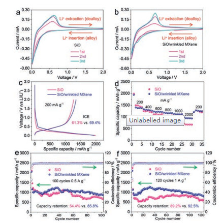
Cyclic voltammetry (CV) was first conducted to understand the electrochemical behavior of the samples (Figs. 4a and b). A cathodic peak at around 1.3 V was detected in the first cycle for SiO (Fig. S5a in Supporting information), which corresponded to the reduction of FEC [45]. However, this peak was stronger for SiO-WM (Fig. S5b in Supporting information), which could be attributed to reduction of FEC and the irreversible reaction caused by the surface functional groups of MXene [46]. A weak and broad cathodic peak at around 0.85 V was observed for both SiO and SiO-WM during the first cycle (Figs. S5c and d in Supporting information), which was attributed to the formation of SEI layer, reduction of SiO to Si and synchronous formation of Li2O and Li silicates [41]. The cathodic peak close to 0 V corresponds to the alloying process of reduced Si with Li to form Li-Si alloys [47]. The anodic peaks located at around 0.37 V and 0.60 V are corresponding to a two-step dealloying process of lithium extraction from Li-Si alloys to Si [47]. The sharper peak shape demonstrated a higher electrochemical activity of SiO-WM than SiO [48, 49]. A cathodic peak near 0.15 V appeared for SiO-WM in the 3rd cycle, which was attributed to the formation of metastable amorphous LixSi phases [50].

|
Download:
|
| Fig. 4. (a, b) CV curves of SiO and SiO-WM at 0.1 mV/s, respectively. (c) The initial charge-discharge curves of SiO and SiO-WM. (d) The rate capability of the samples. (e, f) Cycling performance of the samples at 0.5 and 1 A/g, respectively. | |
The charge-discharge performance was evaluated in 0.01– 2.0 V. The initial charge-discharge curves of SiO and SiO-WM (Fig. 4c) had similar shapes, delivering a discharge specific capacity of 1986.7 and 1945.0 mA h/g at 200 mA/g, respectively. However, the ICE of SiO-WM (69.4%) is higher than that of SiO (61.3%) due to the lower content of SiO in the composite. In addition, SiO-WM also showed a lower polarization, which could be attributed to the better electronic conductivity of SiO-WM than SiO. SiO-WM exhibited better rate capability than SiO (Fig. 4d and Fig. S6 in Supporting information). The initial discharge capacity of SiO at 200, 400, 600, 800, 1000 and 2000 mA/g is 1986.7, 1255.8, 1107.0, 1057.3, 997.2 and 712.9 mAh/g, respectively. The initial discharge capacity of SiO-WM at 200, 400, 600, 800, 1000 and 2000 mA/g is 1945.0, 1327.8, 1230.4, 1183.2, 1128.8 and 984.8 mAh/g, respectively. SiO-WM also has improved cycling performance than SiO (Figs. 4e and f). The cycling curves fluctuated heavily, which was caused by the undulation of ambient temperature. Electrochemical impedance spectroscopy (EIS) results indicated that the charge-transfer impedance of SiO-WM (146.8 Ω) was smaller than that of SiO (184.5 Ω) (Fig. S7 in Supporting information).
The better electrochemical performance of SiO-WM was attributed to the synergistic effect of wrinkled MXene, which not only improved the ICE and electrical conductivity of the composite but also prevented the electrical isolation of active materials in the long cycling performance.
SEM images after 100 cycles at 1 A/g were presented to study the changes of electrode (Fig. S8 in Supporting information). Cracks were found in bare SiO electrode, while not in SiO-WM electrode. The cracks in SiO electrode was attributed to the volume expansion in the cycling performance. For SiO-WM, the wrinkled 2D MXene nanosheets with certain free space could relieve the volume expansion of SiO in the cycling process to some extent, leading to an intact electrode. In addition, a thick layer was formed on the surface of SiO electrode, which may be caused by the more serious side reaction. This thick layer could impede the transport of Li+, leading to a poor rate capability. In contrast, clear particles were observed on the surface of SiO-WM electrode, because SiO particles are encapsulated in wrinkled MXene, which decreased the side reaction to some extent.
In summary, SiO-WM was fabricated by a simple and scalable electrostatic self-assembly method. Under the multiple effect of wrinkled MXene, the SiO-WM exhibited excellent electrochemical performance. Optimizing the content of MXene, adjusting the size of SiO or modifying the electrolyte can definitely further improve the electrochemical performance of the composite, which deserves further investigation. This research provides a multifunctional strategy to address the issues of SiO, paving the way for the commercial application of SiO in energy storage. We believe this strategy can be extended to other Si-based anodes such as Si, SiO2, SiOx and SiOC, which should arose the interest of relevant researchers.
Declaration of competing interestThe authors declare no competing financial interest.
AcknowledgmentsThis work was supported by the National Natural Science Foundation of China (No. 51972198), Shandong Provincial Science and Technology Key Project (No. 2018GGX104002), Taishan Scholars Program of Shandong Province (No. tsqn201812002), Independent Innovation Foundation of Shandong University, the State Key Program of National Natural Science of China (Nos. 61633015, 51532005), the Young Scholars Program of Shandong University (No. 2016WLJH03), the Project of the Taishan Scholar (No. ts201511004), Shandong Provincial Natural Science Foundation (No. ZR2017MB001), Discipline Construction of High-Level Talents of Shandong University (No. 31370089963078), 1000 Talent Plan program (No. 31370086963030) and the National Natural Science Foundation of China (No. 21371108).
Appendix A. Supplementary dataSupplementary material related to this article can befound, in the online version, at doi:https://doi.org/10.1016/j.cclet.2019.12.033.
| [1] |
D. Castelvecchi, E. Stoye, Nature 574 (2019) 308. DOI:10.1038/d41586-019-02965-y |
| [2] |
R.F. Service, Science 366 (2019) 292. DOI:10.1126/science.366.6463.292 |
| [3] |
M. Winter, B. Barnett, K. Xu, Chem. Rev. 118 (2018) 11433-11456. DOI:10.1021/acs.chemrev.8b00422 |
| [4] |
X. Xia, S. Deng, S. Feng, J. Wu, J. Tu, J. Mater. Chem. A: Mater. Energy Sustain. 5 (2017) 21134-21139. DOI:10.1039/C7TA07229E |
| [5] |
S. Shen, X. Xia, Y. Zhong, et al., Adv. Mater. 31 (2019) 1900009. DOI:10.1002/adma.201900009 |
| [6] |
Y. Zhong, X. Xia, S. Deng, et al., Adv. Mater. 30 (2018) 1805165. DOI:10.1002/adma.201805165 |
| [7] |
J. Ni, G. Wang, J. Yang, et al., J. Power Sources 247 (2014) 90-94. DOI:10.1016/j.jpowsour.2013.08.068 |
| [8] |
T. Liu, Y. Zhao, L. Gao, J. Ni, Sci. Rep. 5 (2015) 9307. DOI:10.1038/srep09307 |
| [9] |
J. Ni, Y. Zhao, T. Liu, et al., Adv. Energy Mater. 4 (2014) 1400798. DOI:10.1002/aenm.201400798 |
| [10] |
J. Ni, Y. Zhao, L. Li, L. Mai, Nano Energy 11 (2015) 129-135. DOI:10.1016/j.nanoen.2014.10.027 |
| [11] |
T. Chen, J. Wu, Q. Zhang, X. Su, J. Power Sources 363 (2017) 126-144. DOI:10.1016/j.jpowsour.2017.07.073 |
| [12] |
Z. Liu, Q. Yu, Y. Zhao, et al., Chem. Soc. Rev. 48 (2019) 285-309. DOI:10.1039/C8CS00441B |
| [13] |
T. Xu, Q. Wang, J. Zhang, X. Xie, B. Xia, ACS Appl. Mater. Interfaces 11 (2019) 19959-19967. DOI:10.1021/acsami.9b03070 |
| [14] |
L. Shi, C. Pang, S. Chen, et al., Nano Lett. 17 (2017) 3681-3687. DOI:10.1021/acs.nanolett.7b00906 |
| [15] |
J. Li, L. Wang, F. Liu, et al., ChemistrySelect 4 (2019) 2918-2925. DOI:10.1002/slct.201900337 |
| [16] |
X. Cai, W. Liu, S. Yang, et al., Adv. Mater. Interfaces 6 (2019) 1801800. DOI:10.1002/admi.201801800 |
| [17] |
J. Zhang, J. Zhang, T. Bao, X. Xie, B. Xia, J. Power Sources 348 (2017) 16-20. DOI:10.1016/j.jpowsour.2017.02.076 |
| [18] |
S. Lee, N. Go, J.H. Ryu, J. Mun, J. Electrochem. Sci. Technol. 10 (2019) 244-249. |
| [19] |
H. Zhao, N. Yuca, Z. Zheng, et al., ACS Appl. Mater. Interfaces 7 (2015) 862-866. DOI:10.1021/am507376f |
| [20] |
X. Huang, M. Li, Appl. Surf. Sci. 439 (2018) 336-342. DOI:10.1016/j.apsusc.2017.12.184 |
| [21] |
M. Zhou, M.L. Gordin, S. Chen, et al., Electrochem. commun. 28 (2013) 79-82. DOI:10.1016/j.elecom.2012.12.013 |
| [22] |
J. Zhang, J. Zhang, T. Bao, X. Xie, B. Xia, J. Power Sources 348 (2017) 16-20. DOI:10.1016/j.jpowsour.2017.02.076 |
| [23] |
X. Liao, M. Peng, K. Liang, J. Electroanal. Chem. Lausanne 841 (2019) 79-85. DOI:10.1016/j.jelechem.2019.04.040 |
| [24] |
Q. Pan, P. Zuo, T. Mu, et al., J. Power Sources 347 (2017) 170-177. DOI:10.1016/j.jpowsour.2017.02.061 |
| [25] |
Z. Lin, J. Li, Q. Huang, et al., J. Phys. Chem. C 123 (2019) 12902-12909. |
| [26] |
M. Xia, Y. Li, Y. Wu, et al., Appl. Surf. Sci. 480 (2019) 410-418. DOI:10.1016/j.apsusc.2019.02.207 |
| [27] |
X. Xia, S. Deng, D. Xie, et al., J. Mater. Chem. A Mater. Energy Sustain. 6 (2018) 15546-15552. DOI:10.1039/C8TA06232C |
| [28] |
Y. Zhang, X. Xia, B. Liu, et al., Adv. Energy Mater. 9 (2019) 1803342. DOI:10.1002/aenm.201803342 |
| [29] |
Y. Xia, T.S. Mathis, M. Zhao, et al., Nature 557 (2018) 409-412. DOI:10.1038/s41586-018-0109-z |
| [30] |
L. Yu, L. Hu, B. Anasori, et al., ACS Energy Lett. 3 (2018) 1597-1603. DOI:10.1021/acsenergylett.8b00718 |
| [31] |
C. Wei, H. Fei, Y. Tian, et al., Small 15 (2019) 1903214. DOI:10.1002/smll.201903214 |
| [32] |
J. Pang, R.G. Mendes, A. Bachmatiuk, et al., Chem. Soc. Rev. 48 (2019) 72-133. DOI:10.1039/C8CS00324F |
| [33] |
C. Zhang, S. Park, A. Seral-Ascaso, et al., Nat. Commun. 10 (2019) 849. DOI:10.1038/s41467-019-08383-y |
| [34] |
Y. Tian, Y. An, J. Feng, ACS Appl. Mater. Interfaces 11 (2019) 10004-10011. DOI:10.1021/acsami.8b21893 |
| [35] |
M. Alhabeb, K. Maleski, B. Anasori, et al., Chem. Mater. 29 (2017) 7633-7644. DOI:10.1021/acs.chemmater.7b02847 |
| [36] |
H. Chen, L. Yu, Z. Lin, et al., J. Mater. Sci. 55 (2020) 1148-1156. DOI:10.1007/s10853-019-04003-8 |
| [37] |
X. Xie, M. Zhao, B. Anasori, et al., Nano Energy 26 (2016) 513-523. DOI:10.1016/j.nanoen.2016.06.005 |
| [38] |
D. Zhao, M. Clites, G. Ying, et al., Chem. Commun. (Camb.) 54 (2018) 4533-4536. DOI:10.1039/C8CC00649K |
| [39] |
C. Wei, H. Fei, Y. An, Y. Zhang, J. Feng, Electrochim. Acta 309 (2019) 362-370. DOI:10.1016/j.electacta.2019.04.094 |
| [40] |
Y.T. Liu, P. Zhang, N. Sun, et al., Adv. Mater. 30 (2018) 1707334. DOI:10.1002/adma.201707334 |
| [41] |
T. Xu, J. Zhang, C. Yang, et al., J. Alloy. Compound. 738 (2018) 323-330. DOI:10.1016/j.jallcom.2017.12.162 |
| [42] |
X. Zhao, M. Liu, Y. Chen, et al., J. Mater. Chem. A Mater. Energy Sustain. 3 (2015) 7870-7876. DOI:10.1039/C4TA07101H |
| [43] |
P. Zhang, D. Wang, Q. Zhu, et al., Nano-Micro Lett. 11 (2019) 81. DOI:10.1007/s40820-019-0312-y |
| [44] |
F. Cheng, G. Wang, Z. Sun, et al., Ceram. Int. 43 (2017) 4309-4313. DOI:10.1016/j.ceramint.2016.12.074 |
| [45] |
C. Xu, F. Lindgren, B. Philippe, et al., Chem. Mater. 27 (2015) 2591-2599. DOI:10.1021/acs.chemmater.5b00339 |
| [46] |
F. Kong, X. He, Q. Liu, et al., Electrochem. commun. 97 (2018) 16-21. DOI:10.1016/j.elecom.2018.10.003 |
| [47] |
W. Wu, Y. Liang, H. Ma, Y. Peng, H. Yang, Electrochim. Acta 187 (2016) 473-479. DOI:10.1016/j.electacta.2015.11.008 |
| [48] |
Y. Zeng, Z. Lin, Z. Wang, et al., Adv. Mater. 30 (2018) 1707290. DOI:10.1002/adma.201707290 |
| [49] |
Z. Yao, X. Xia, D. Xie, et al., Adv. Funct. Mater. 28 (2018) 1802756. DOI:10.1002/adfm.201802756 |
| [50] |
X. Chen, X. Li, F. Ding, et al., Nano Lett. 12 (2012) 4124-4130. DOI:10.1021/nl301657y |