 2020, Vol. 31


Considerable interest has been recently given to the incorporation of the emergent carbon material graphene as fundamental building blocks in both science and technology communities, especially in the electronic device application [1-4], However, controllable the bandgap of semimetal graphene is still need to be addressed to fully utilize this material. Doping of graphene is now considered to be the easiest way to control its electrical property [5, 6]. Nitrogen doping is a promising way to modulate the electrical properties of graphene to realize graphene-based electronics and promise fascinating properties and applications. Several strategies have been successfully reported to get nitrogen-doped (N-doped) graphene including chemical vapor deposition (CVD)-growth [7], electrochemistry [8] and plasma treatment [9]. N-doped graphene has been used in edge doping investigation [10], high-performance electrical devices [11], and metal-free electrocatalyst for oxygen reduction reaction [12].
Because of the sensitivity of graphene to local perturbations, noncovalent latching of functional molecules on graphene surface provides a means to tuning the electronic structure of graphene. Functionalization of graphene by noncovalent bonding does not basically generate defects. Furthermore, function molecules offer the additional flexibility of introducing stimuli-responsive sites and easily create reversible regulation, which opens up new routes to develop desirable transistors [13]. Recently several groups reported using this noncovalently method to fabricate reversible graphene transistors [14-16].
Graphene filed-effect transistors (FET) devices are becoming one of the hottest areas in potential diverse applications of electronics in switching, sensing and detecting system sowing to its ultrahigh carrier mobility, the ideal two-dimensional structure, and the simple fabrication process compatible with the standard planar Si technology [17, 18]. Graphene has the simplest chemical composition and atomic bonding configuration in a 2D manner that maximizes its surface-to-volume ratio. Each carbon atom on the surface of graphene is exposed to the environment and any tidy changes could cause drastic changes in its electrical properties. In conjunction with the high sensitivity of graphene transistor, the flexible noncovalently functionalization strategy and the specific electronic structure of N-doped graphene transistors can be applied as a promising platform for creating new types of sensors and multifunctional devices.
Herein, we demonstrate reversible regulation of N-doped graphene with sequential chemical treatment by adsorption and desorption of titanium(Ⅳ) bis(ammoniumlactato) dihydroxide (Ti complex). The substitution doping nitrogen effectively affected the electrical structure of graphene and successfully became the absorbed centers of Ti complex by electrostatic interaction. As the molecules reversible assembly, the current of the device also changes which shows significant switching effect. By using Raman spectroscopy and electrical measurements, we investigate the chemical induced sensing effect. The dynamic information of the switching process provides powerful understanding to further optimize the devices. The advantage of this easy and efficient way to control the carrier of N-doped graphene can also thrust their applications in other fields, such as optoelectronic and fuel cell devices.
First of all, we synthesized the nitrogen-doped graphene through a modified chemical vapor deposition (CVD) process which we reported before [12]. Briefly, a thin layer of nickel (~300 nm) was deposited on a SiO2/Si substrate with sputter coating. The Ni-coated SiO2/Si wafer was then heated up within a quartz tube furnace. A nitrogen-containing reaction gas mixture (NH3:CH4:H2:Ar = 10:50:65:200 sccm) was introduced into the quartz tube and kept flowing for 5 min, followed by purging with a flow of NH3 and Ar only for another 5 min. The resultant N-doped graphene film can be easily etched off from the substrate by a standard nondestructive polymer transfer [19]. The as-grown graphene films were spin-coated with a thin layer of poly(methyl methacrylate) (PMMA) which was diluted using anisole. Sub-sequently, the underlying Ni was etched away by for 2–4 h etching in hydrochloric acid (HCl). The PMMA/graphene film was then transferred to DI water and left overnight to remove the residual etchant. Finally, the PMMA/graphene film was transferred to silicon substrate and blow-dried gently with nitrogen gas. The PMMA was removed in a boiling acetone solution.
Next the device was fabricated on a degenerately doped silicon substrate with 400 nm thick thermally grown SiO2 layer [20]. To aid in the alignment for the following photolithographic process, gold marks were thermally evaporated through a shadow mask. In order to form graphene sheets, selective water plasma was applied through a photo lithographically-patterned resist mask to etch away the deprotected graphene. Finally, after another photolithographic process, high-density patterned metallic electrodes (5 nm of Cr followed by 50 nm of Au) which separated by 5 μm in the center were deposited onto the graphene sheets through thermal evaporation. The doped silicon wafer served as a global back-gate electrode for the devices. Mass-producing graphene transistors with high quality and high yield were made using this method. The electrical characteristics of the transistors were measured at room temperature in the ambient atmosphere by probe station (1160 Series, Signatone) connected with a semiconductor parameter analyzer (2636A, Keithley). The graphene, bridging the source and drain electrodes, behaved as the conducting channel. With the metal pads as source (S) and drain (D) contacts, by applying gate bias voltage from the silicon substrate as the global back-gate, the electrical properties of graphene devices can be tuned.
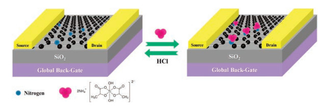
After fabrication, the N-doped graphene FETs were then directly functionalized by self-assemble of Ti complex from solution. Previous research has revealed that the N-doped sites in carbon nanotube successfully nucleated the biomimetic mineralization of a uniform nanoscale thick TiO2 shell with strong interaction with Ti molecules [21]. Graphene has the same structure similar as carbon nanotube, the N-doped sites also provide the binding sites for Ti complex. Besides, in this complex, hydroxyl is one kind of strong electron donating group, when doped onto the surface of graphene, the conductivity of graphene would be modulated by surface charge transfer between graphene and the Ti complex. Prior to assembly, the pristine N-doped graphene devices were immerged in ethanol for 1 min to enhance wettability. Then the devices were placed in the water solution of Ti complex. After immersion of the devices for around 10 min in the solution (ca. 0.1 g/mL), they were removed from the solution and washed with fresh water several times. Fig. 1 shows a simple scheme of a typical N-doped graphene transistor functionalized with Ti complex.

|
Download:
|
| Fig. 1. Schematic depiction of the structures of the back-gated N-doped graphene transistors used in this study and how the Ti complex functionalized reversible chemical switch works. | |
Raman spectroscopy is a powerful and noninvasive tool for identifying carbon material. Fig. 2 shows the Raman spectra of an individual device before and after assembly. The spectra were obtained using a micro-Raman spectroscope (Renishaw), with excitation energy of 2.41 eV (514 nm), a 1 μm excitation spot size and wave number calibration was done using a reference Si peak at 520 cm-1. A single symmetric 2D peak, a small G/2D ratio, and a very clear D peak were observed after N-doped graphene transfer to the silicon substrate which strongly suggest that the graphene was a few layers from the G/2D intensity ratio. N-doped graphene has a clear D band (ca. 1353 cm-1), which indicated the N doping of the graphitic sheets and introduced large amount of topological defects [22]. As shown in Fig. 2b, after assembly the Ti complex, the G peak shifted about 3 cm-1. There are many factors which can affect the position of G band, such as doping [23], defects [24], layer numbers [25]. The G band shift here indicated that N-doped graphene was potentially doped by Ti complex. Moreover, the ID/IG intensity also changed from 0.66 to 0.88 which was shown in Fig. 2c which proved that Ti complex had successfully absorbed on the graphene surface. The Ti complex was attached to the graphene surface by electrostatic interaction and hydrogen bonding which has been demonstrated already [21]. To further confirm the successful assembly of Ti complex on graphene, we treatment of the device with HCl in which the physical absorbed Ti complex can be washed away. After further immersion the device in 0.1 mol/L HCl, in situ Raman was measured. After HCl treatment, the shift in G band was reversed back and the ID/IG intensity also recovered to 0.76 which was caused by desorption of the Ti complex. From all the results, the reversible Raman changes can be clearly attributed to the absorption and desorption of Ti complex.

|
Download:
|
| Fig. 2. (a) In situ Raman spectra of an individual nitrogen-doped graphene (black), after Ti complex assembly (red) and after HCl treatment (blue) at wavelength of 514 nm. Change of (b) the G band position and (c) ID/IG intensity in different condition. | |
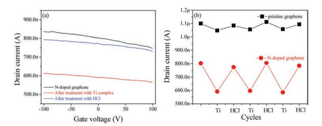
Then we measured the electrical characteristics of the functionalized N-doped graphene FETs to check the effect of Ti complex. We found that the conductance of these transistors changed significantly after self-assembly. To carry out the measurement efficiently, all the electric measurement was under the same condition. Fig. 3a shows the source-drain current (ID) as a function of the gate voltage (VG) at a fixed source-drain bias voltage (VD = 1 mV) a representative device in each step of the operations. To eliminate possible artifacts from gate hysteresis, all of the current-voltage (I–V) curves were acquired on the same measurement cycle while scanning from positive to negative bias. We observed very stable I–V curves for these devices in fixed experimental conditions, and then they can be used as the platform for chemical sensor. We note that, owing to chemical doping and/or charge transfer induced by etching agents and polymer resists (iron chloride and PMMA), the resulting N-doped graphene only behave as p-type semiconductors, as shown in black curve in Fig. 3a [26]. The electrical properties of N-doped graphene FETs show different types according to diverse synthesis method and device fabrication technology [27]. According to the Raman spectra, the N-doped graphene used in the study was a few layers, so the gate modulation was weak here. As shown in red curve in Fig. 3a, after Ti complex were absorbed on the surface of N-doped graphene by electrostatic interaction, the devices showed significant conductance decrease. We tested more than 30 devices, and found the decrease of conductance was universal for N-doped graphene transistors after Ti complex self-assemble. Hole dominates the carrier transition in p-type semiconductor, the conductance decrease was supposed to attribute to the charge transfer between the Ti complex and N-doped graphene in which the net negative charge was transferred from Ti complex toN-dopedgraphene.Onthe other hand, the absorbed Ti complex also became the scattering centers of the holes carrier. Both two mechanisms caused the conductance decrease of the N-doped graphene transistors [28, 29]. These results are consistent with those obtained from the Raman results that the ID/IG intensity ratio increased after Ti complex functionalized which implied that the Ti complex anchored to the surface of N-doped graphene successfully.

|
Download:
|
| Fig. 3. (a) The changes in drain current of a typical N-doped graphene transistor functionalized by Ti complex as a function of VG at different states: N-doped graphene (black), after Ti complex assembly on graphene surface (red), after the treatment of hydrochloric acid (blue). Inset shows an optical image of the N-doped graphene transistors used in this study in which the metallic electrodes separated by 5μm in the center and the zoomed-in image of the part labeled by a blue square. (b) The switching cycles for the same device (red) and a control pristine graphene transistor (black) upon sequential treatment with Ti complex and hydrochloride acid (all current values were taken at VG = 0 V). All the measurements were carried out at VD = 1 mV. | |
Interestingly, when the Ti complex was washed away by HCl, reversible and significant change in ID was observed for the N-doped graphene transistors. Fig. 3a exhibited such a chemical induced reversible switching effect in an individual device with sequential treatment the transistor with Ti complex and HCl. When the Ti complex was washed away, the conductance increased, as the blue curve shown in Fig. 3a, and recovered almost to the original high value. Noticeably, the current switching effect is reversible and reproducible and can be used as a chemical sensor. Fig. 3b showed such three representative reversible drain current switching cycles of the same device shown in Fig. 3a at fixed VG when sequential treatment the N-doped graphene transistor with Ti complex and HCl. After Ti complex absorption, the drain current of the transistor decrease to its low conductance state, while after washing the Ti complex, the current recovered to the original conductance high state. The switching process was reversible over several cycles in sequential chemical treatments. These current switching phenomena were quite reproducible because all the 30 tested devices showed the similar results. The stability of the electrodes is very well after treated with hydrochloric acid for several times.
Nitrogen was reported to have essential role as the binding sites for Ti complex and tune the electronic structure of graphene [21]. To confirm the effect of nitrogen, we used pristine CVD growth graphene transistor as control. In this case, we are able to characterize and compare the chemical induced response of both pristine and N-doped graphene devices at the same conditions. As shown in Fig. S2 (Supporting information), under sequential treatment with Ti complex and HCl, the control transistor showed slightly change because of the sensitivity of the graphene surface. Fig. 3b also exhibited the cycles of the control device with pristine graphene in the same treatments. The pristine graphene also behaved as a p-type semiconductor, and showed higher conductivity than N-doped graphene. The N-doped graphene shows obvious much larger conductance change than pristine graphene which further confirmed that N-doped graphene was a better material using in sensing applications. To further rule out the potential artifact induced by treatment of HCl, we also conducted control experiments that N-doped graphene transistors were directly treatment with HCl at the same condition. As shown in Fig. S1 (Supporting information), we found that after immersion in 0.1 mol/L HCl, slight conductance decrease was observed for the control device, which was in contrary to the change of the devices mentioned above. These results eliminated the doping effect of hydrochloride acid and proved that the Ti complex played an important role in regulating the conductance of N-doped graphene.
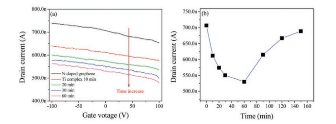
To further understand the dynamic process of the switching effect, we investigated the time-dependent in another individual N-doped transistor with 0.1 g/mL Ti complex. Fig. 4a shows the change of I–V curves in each step under Ti complex self-assembly. We found the back-and-forth switching effect was gradual in time as shown in Fig. 4a. The drain current decreased gradually as the increasing immersion time of Ti complex. The conductance sharply decreased at the beginning 10 min mainly due to much doping sites on the surface which could adsorb more Ti complex. But after that, with time increase, all the potential binding sites were occupied by Ti complex, so the conductance tended to be saturated gradually. On the contrary, after the transistor reached to its lowest conductance and further treatment with HCl, the device presented a slower relaxation. After another ~100 min, the device recovered to its original conductance. This can be explained by the different rate between adsorption and desorption of Ti complex on N-doped graphene. Fig. 4b presented the whole cycles with the chemical treatment according to the dynamic time-dependent test of Fig. 4a using the drain current at fixed gate voltage.

|
Download:
|
| Fig. 4. (a) The changes in drain current of another N-doped graphene transistor assembled by Ti complex as a function of VG in increasing time. (b) A whole switching cycle for the same device on sequential treatment with Ti complex and HCl (all current values were taken at VG = 0 V). All the measurements were carried out at VD = 1 mV. | |
Then we turned on our attention to the relationship between current change and concentration-dependent of Ti complex. Using three different concentration of Ti complex, we detected the current change of individual N-doped graphene transistors in continuous treatments. All the results were summarized in Fig. 5, we calculated the ratio (%) of the current change (ΔI) to the initial value (I0). In the first 10 min, the current change improved with the concentration increase. But after about 30 min incubation, the current change became similar to ~20% to reach the saturation. In low Ti complex concentration (0.05 g/mL), the current change shows nearly linear increase, while for high concentration (0.2 g/mL), the current decreased quickly at the beginning, then reduced the change slope, which most likely due to the dynamic equilibrium of the Ti complex in solution. Ti complex can regulate the conductance of N-doped graphene transistor observably, the dynamic analysis may provide the optimal condition to functionalize the device and develop desirable transistor or sensors.

|
Download:
|
| Fig. 5. The current changes of N-doped graphene transistors with time increase in different concentration from 0.05 g/mL, 0.1 g/mL to 0.2 g/mL. | |
In conclusion, we have shown an approach to achieve reversible regulation the conductance of N-doped graphene using non-covalent assembly of molecules on graphene surface. Raman analysis and transistor characteristics show significant switching effect under sequential chemical treatment. The adsorption of Ti complex on nitrogen binding sites dominates the conductance change of the transistors. The sensitivity of the sensing properties can be further optimized according to the dynamic analysis of the switching process. These studies create new avenue to chemical functionalization graphene devices to creat stable and stimuliresponsive reversible transistors. Moreover, all the results demonstrate that N-doped graphene is a more powerful material for sensing application than pristine graphene. This simple and efficient method in tuning the electronic devices provides promising potential for a wide variety of device applications in both the industrial and scientific communities.
Appendix A. Supplementary dataSupplementary material related to this article can be found, in the online version, at doi:https://doi.org/10.1016/j.cclet.2019.05.014.
| [1] |
K.S. Novoselov, A.K. Geim, S.V. Morozov, et al., Science 306 (2004) 666-669. DOI:10.1126/science.1102896 |
| [2] |
R. Raccichini, A. Varzi, S. Passerini, B. Scrosati, Nat. Mater. 14 (2014) 271-279. |
| [3] |
V. Georgakilas, J.N. Tiwari, K.C. Kemp, et al., Chem. Rev. 116 (2016) 5464-5519. DOI:10.1021/acs.chemrev.5b00620 |
| [4] |
Y. Cao, V. Fatemi, S. Fang, et al., Nature 556 (2018) 43-50. DOI:10.1038/nature26160 |
| [5] |
S. Kawai, S. Saito, S. Osumi, et al., Nat. Commun. 6 (2015) 8098. DOI:10.1038/ncomms9098 |
| [6] |
T.H. Han, S.J. Kwon, N. Li, et al., Angew. Chem. Int. Ed. 55 (2016) 6197-6201. DOI:10.1002/anie.201600414 |
| [7] |
S.M. Shinde, E. Kano, G. Kalita, et al., Carbon 96 (2016) 448-453. DOI:10.1016/j.carbon.2015.09.086 |
| [8] |
L. Gan, D. Zhang, X. Guo, Small 8 (2012) 1326-1330. DOI:10.1002/smll.201102302 |
| [9] |
M. Rybin, A. Pereyaslavtsev, T. Vasilieva, et al., Carbon 96 (2016) 196-202. DOI:10.1016/j.carbon.2015.09.056 |
| [10] |
X. Wang, X. Li, L. Zhang, et al., Science 324 (2009) 768-771. DOI:10.1126/science.1170335 |
| [11] |
H. Kim, J. Byun, S.H. Bae, et al., Adv. Energy Mater. 6 (2016) 1600172. DOI:10.1002/aenm.201600172 |
| [12] |
L. Qu, Y. Liu, J.B. Baek, et al., ACS Nano 4 (2010) 1321-1326. DOI:10.1021/nn901850u |
| [13] |
F. Schedin, A.K. Geim, S.V. Morozov, et al., Nat. Mater. 6 (2007) 652-655. DOI:10.1038/nmat1967 |
| [14] |
J. Kim, M.S. Lee, S. Jeon, et al., Adv. Mater. 27 (2015) 3292-3297. DOI:10.1002/adma.201500710 |
| [15] |
S. Liu, S. Jamali, Q. Liu, et al., Macromolecules 49 (2016) 7434-7441. DOI:10.1021/acs.macromol.6b01011 |
| [16] |
X. Wang, X. Liu, H. Yuan, et al., Mater. Design 139 (2018) 372-379. DOI:10.1016/j.matdes.2017.11.023 |
| [17] |
S. Kumar, W. Ahlawat, R. Kumar, et al., Biosens. Bioelectron. 70 (2015) 498-503. DOI:10.1016/j.bios.2015.03.062 |
| [18] |
Z. Zhu, Nano-Micro Lett. 9 (2017) 25. DOI:10.1007/s40820-017-0128-6 |
| [19] |
K.S. Kim, Y. Zhao, H. Jang, et al., Nature 457 (2009) 706-710. DOI:10.1038/nature07719 |
| [20] |
Y. Cao, S. Dong, S. Liu, et al., Angew. Chem. Int. Ed. 51 (2012) 12228-12232. DOI:10.1002/anie.201205607 |
| [21] |
W.J. Lee, J.M. Lee, S.T. Kochuveedu, et al., ACS Nano 6 (2012) 935-943. DOI:10.1021/nn204504h |
| [22] |
Y.T. Lee, N.S. Kim, S.Y. Bae, et al., J. Phys. Chem. B 107 (2003) 12958-12963. DOI:10.1021/jp0274536 |
| [23] |
S.S. Nanda, M.J. Kim, K.S. Yeom, et al., Trac-Trend. Anal. Chem. 80 (2016) 125-131. DOI:10.1016/j.trac.2016.02.024 |
| [24] |
R. Beams, L. Gustavo Cançado, L. Novotny, J. Phys.-Condens. Mat. 27 (2015) 083002. DOI:10.1088/0953-8984/27/8/083002 |
| [25] |
X.L. Li, X.F. Qiao, W.P. Han, et al., Nanoscale 7 (2015) 8135-8141. DOI:10.1039/C5NR01514F |
| [26] |
L. Gan, S. Liu, D.N. Li, et al., Acta Phys.-Chim. Sin. 26 (2010) 1151-1156. |
| [27] |
T. Kato, R. Hatakeyama, ACS Nano 6 (2012) 8508-8515. DOI:10.1021/nn302290z |
| [28] |
S. Myung, A. Solanki, C. Kim, et al., Adv. Mater. 23 (2011) 2221-2225. DOI:10.1002/adma.201100014 |
| [29] |
S. Mao, G. Lu, K. Yu, Z. Bo, J. Chen, Adv. Mater. 22 (2010) 3521-3526. DOI:10.1002/adma.201000520 |