 2020, Vol. 31


b School of Materials Science and Energy Engineering, Foshan University, Foshan 528000, China
Past decades have witnessed the great progress of fluorescent colloidal nanostructures [1-3]. High-quality fluorescent colloidal nanocrystals (NCs), like cadmium chalcogenides, are one answer to many envisioned applications, such as light-emitting devices [4], biological labels [5] and sensors [6]. More recently, the perovskite nanocrystals, especially all-inorganic perovskite nanocrystals, have become an important family of fluorescent nanomaterials due to their remarkable optical and optoelectronic properties [7-9]. Nevertheless, the optical nature of fluorescent nanocrystals is highly determined by the interfacial chemical environment [10]. Poor surface passivation of organic ligands and surface defects (e.g., dangling bonds) will enhance the trap state emission or nonradiative recombination and consequently reduce the photoluminescence quantum yield(PLQY) [11]. There are several methodologies to optimize the interfacial chemical environment of NCs. For example, ligand exchange can efficiently improve the performance of NCs when used for optoelectronic devices [12, 13]. Another feasible route of designing heterostructures such as core-shell NCs, which are usually classified as type-Ⅰ, reverse type-Ⅰ and type-Ⅱ structures, is well suited for protecting the luminescent NCs from detrimental chemical environment [14-16]. Type-Ⅰ NCs are such materials that the conduction band of the shell is of higher energy than that of the core, while the valence band of the shell is of lower energy than that of the core, leading to both electrons and holes confined in the core [17]. As its name implies, reverse type-Ⅰ NCs present opposite energy distribution of valence band and conduction band to type-Ⅰ NCs, with both electrons and holes tending to be confined in the shell [18]. As for type-Ⅱ NCs, both the valence and conduction bands in the core are lower (or higher) than that of the shell, therefore one carrier (e.g., electron) is mostly confined to the core, while the other is mostly confined to the shell [19]. Among a great variety of type-Ⅰ core-shell nanostructures, CdSe/CdS (core/shell) NCs were proven to be very promising for the photoluminescent applications and have been widely researched [20, 21].
Several methodologies have been developed for synthesizing CdSe/CdS (core/shell) NCs [22-24], and the most typical route of them is the successive ion layer adsorption and reaction (SILAR) strategy. For instance, Peng et al. reported several monolayers of CdS shell growing on CdSe core at 220–240 ℃ with PLQY ranging from 20% to 40% [25]. This strategy requires a precise control of the amounts of the precursors in each half-reaction, which are calculated to match on single monolayer coverage for cores in solution. At the same time, the highly reactive metal and chalcogenide precursors required a relative high temperature to allow for the growth of the shell and to suppress homogenous nucleation [26]. As a result, several works focusing on the synthesis of CdSe/CdS (core/shell) NCs at room temperature were reported [27-29]. For example, Talapin and his colleagues utilized K2S and Cd(OAc)2 to grow multiple CdS monolayers on CdSe NCs by a tedious and sequential atomic layer deposition strategy [30]. Nonetheless, it is still a challenge to achieve highly luminescent CdSe NCs under facile and moderate treatment conditions.
Herein, we developed a mild and efficient strategy to improve the luminescentproperty of as-synthesized CdSe nanostructures (including quantum dots and nanorods) based on dual-layer passivation of CdS shell and organic ligands. Excluding the high temperature and organometallic reagents used in typical synthetic strategy like SILAR, our methodology was capable of forming a monolayer or sub-monolayer CdS shell on CdSe core by S2− ligand exchange followed by binary ligand passivation through a phase-transfer procedure under ambient conditions. After 30-min incubation, the PLQY of CdSe/CdS (core/shell) nanostructures was dramatically enhanced up to ∼70% and their morphology kept intact after all the procedures. The enhancement of PLQY was proven to be versatile, regardless of the morphology (nanorods or quantum dots), crystal structure (wurtzite or zinc-blende) or size (from 2.1 nm to 7.7 nm) of CdSe NCs.
Materials: Selenium powder (Se, 99.5%), oleic acid (OA, 90%), oleylamine (OAm, 70%), 1-octadecene (ODE, 90%), tri-n-octylphosphine (TOP, 90%), tri-n-butylphosphine (TBP, 97%), tri-n-octylphosphine oxide (TOPO, 90%), and tetradecylphosphonic acid (TDPA, 97%) were purchased from Sigma-Aldrich. Cadmium oxide (CdO, 99.99%) and ammonium sulfide [(NH4)2S] solution (40–48 wt% in water) were purchased from Aladdin. Formamide (FA), toluene, absolute ethanol, and n-hexane were purchased from Sinopharm Chemical Reagent Co., Ltd. All reagents were used without further purification.
Synthesis of CdSe Nanorods (NRs): All preparative procedures were conducted using standard Schlenk-line techniques under N2. CdSe NRs capped with TOP, TBP, TDPA, and TOPO. In a typical synthesis, 105 mg of CdO, 449 mg of TDPA and 1.13 g of TOPO were heated to 100 ℃ and degassed for 30 min, and then heated to 300 ℃ until becoming clear under N2. The Cd precursor was cooled to room temperature and aged for 24 h under N2. After that, the solution was heated to 320 ℃, while Se precursor solution containing 31 mg of Se, 723 mg of TOP, 95 mg of TBP and 150 mg of toluene was swiftly injected. The reacting mixture was cooled to 250 ℃ and kept the temperature for 1 h. After cooling down to room temperature, crude solution was mixed with absolute ethanol and centrifuged. The precipitation was dispersed in n-hexane to form a stable solution.
S2− treatment and binary ligand passivation: A stock solution of (NH4)2S in FA was prepared by adding 10 μL of (NH4)2S aqueous solution into 1 mL of FA. 5 mL of CdSe NC solution (∼ 0.01 mol/L) in hexane was mixed with 1 mL of (NH4)2S stock solution. The resulting mixture was stirred for 10 min, and CdSe NCs were completely transferred into the FA phase. CdSe NCs capped with S2− in FA were then mixed 5 mL of n-hexane, 1 mL of OAm and 1 mL of TOP. After stirring vigorously, the CdSe NCs were transferred into the hexane phase again with the assistance of OAm and TOP ligands. The as-obtained solution was incubated for 30 min. All procedures were conducted under ambient conditions.
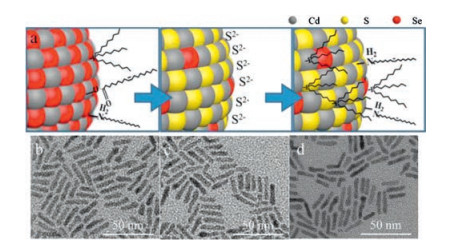
The monodisperse and size-tunable CdSe cores, including NRs and quantum dots(QDs), are synthesized via literature methods [31-33]. As illustrated in Fig. 1a, the procedure of PL enhancement primarily based on modifications of our previous work [34] and could be defined as two basic steps, S2− substitution and organic ligand passivation. First of all, the as-synthesized CdSe cores dispersed in the non-polar solvent were mixed with S2− dissolved in the polar solvent. Notably, S2− could not only replace the original ligands capped on CdSe cores but also substitute the superficial Se2− to afford a monolayer or sub-monolayer CdS shell (denoted as CdSe/CdS/S2−). After that, the polar phase containing CdSe/CdS/S2− nanostructureswas mixed with two types of organic ligands, oleylamine (OAm) and tri-n-octylphosphine (TOP), dispersed the non-polar solvent. The following exchange between S2− and the binary ligands transferred CdSe/CdS nanostructures back into the non-polar phase, which were re-capped with the organic ligands (denoted as CdSe/CdS/OAm-TOP).

|
Download:
|
| Fig. 1. (a) Schematic illustration of S2- exchange and binary ligand passivation; TEM images of (b) pristine CdSe NRs, (c) CdSe/CdS/S2- CdSe NRs and (d) CdSe/CdS/OAm-TOP NRs. | |
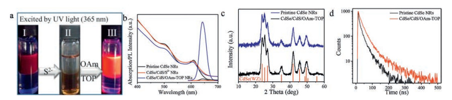
The contour size of typical CdSe NRs used in our work was ca. 18.9 nm × 3.9 nm (Fig. 1b). As is shown in Figs. 1c and d, transmission electron microscopy (TEM) indicates that the morphology of CdSe NRs remains unchanged after the procedure of S2−coordination and replacement (Fig. 1c) and organic ligands coordination (Fig. 1d). The high-resolution TEM (HRTEM) images of CdSe NRs before and after treatment were provided in Fig. S1 (Supporting information), in which no obvious change of the CdSe lattice was observed. However, the PL intensity of CdSe NRs apparently increases up after the last step according to visual observation under UV light source (Fig. 2a). To quantitatively measure the enhancement of PL intensity, UV–visspectroscopy and fluorescence spectroscopy tests were conducted on each stage of the CdSe NRs. Fig. 2b shows the normalized UV–vis and PL spectra of the CdSe NRs, where UV–vis absorption spectra changed slightly while the main peak of PL intensity first decreased under the S2− treatment (QY = ∼0.03%) and then drastically increased up after organic ligands coordination. The PLQY of CdSe NRs was measured to be improved from 0.2% (pristine CdSe NRs) to 37.6% (CdSe/CdS/OAm-TOP NRs) using Rhodamine 6 G as a reference standard (QY = 95% in ethanol), corresponding to approximately 188 times increase. In addition, the PL enhancement of our methodology could be completed in 30-min incubation, without requiring photo annealing or any other post-treatment. Notably, the PLQY of our CdSe/CdS/OAm-TOP NRs is comparable to that of CdSe/CdS core/shell NRs reported by Talapin et al. [30].

|
Download:
|
| Fig. 2. (a) Photographs of the treated CdSe NRs under UV light (365 nm); (b) Normalized UV–vis absorption and PL emission spectra at each stage of CdSe NRs; (c) XRD patterns of pristine CdSe NRs and CdSe/CdS/OAm-TOP NRs. The XRD stick pattern of WZ-CdSe is also provided for reference (JCPDS No. 00-002-0330); (d) Time-dependent PL decays of pristine CdSe NRs and CdSe/CdS/OAm-TOP NRs | |
The crystalline structures of pristine CdSe NRs and CdSe/CdS/OAm-TOP NRs were characterized by powder X-ray diffraction (XRD) analysis. As shown in Fig. 2c, the XRD patterns of both samples are in consistence with standard CdSe crystal with a wurtzite (WZ) structure, indicating that the S2− treatment step did not change the crystal structure of CdSe core. To further explore the structural evolution of CdSe NRs, energy-dispersive X-ray spectroscopy (EDS) mapping was employed to analyze the elemental composition and distribution (Fig. S2 in Supporting information). The average atomic percentages of Cd, Se and S were calculated and displayed in Table S1 (Supporting information). As expected, the atomic ratio of Cd/Se in pristine CdSe NRs is approximately 1:1. After the treatment, we observed that a portion of Se on the CdSe NRs was replaced by S, forming the CdSe/CdS (core/shell) structures. The time-dependent PL decay spectra (Fig. 2d) showed that the radiative lifetimes of pristine CdSe NRs and CdSe/CdS/OAm-TOP NRs were 22 and 35 ns, respectively. The prolonged lifetime indicates the excellent passivation of CdS shell and organic ligands, which accounts for the reduction of surface defects.
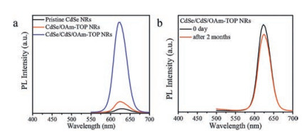
Previous studies [35] have demonstrated that the presence of binary ligands is able to enhance the QY of semiconductor NCs, thus we designed a control experiment to evaluate the contribution originating from the binary ligands. As shown in Fig. 3a, the normalized PL spectrum of CdSe NRs, which were only treated with binary ligands of OAm and TOP, was compared with those of pristine CdSe NRs and CdSe/CdS/OAm-TOP NRs. We concluded that the binary ligands did have positive effect improving the PLQY (from 0.2% to 4.5%), however, S2− treatment was still the dictating factor for the enhanced PLQY. We also found that other tertiary phosphines, like tri-n-butylphosphine (TBP), could replace TOP and play similar roles in the passivation of CdSe NRs (Fig. S3 in Supporting information). Besides the enhancement of QY, the CdSe/CdS/OAm-TOP NRs exhibit high stability against detrimental oxygen, which is one significant cause of the inactivation of luminescent semiconductor NCs. The as-obtained CdSe/CdS/OAm-TOP NRs solution was exposed to ambient environment in darkness for 2 months, and the QY of that sample only decreased from 37.6% to ∼33%, without any shift of the main peak in PL spectrum (Fig. 3b). We also conducted control experiments (Fig. S4 in Supporting information), in which the PL intensity of the pristine CdSe NRs decreased dramatically after only 7 days under the same condition. The result further demonstrates that the passivation of CdS shell and organic ligands can efficiently protect the CdSe NRs from oxidation.

|
Download:
|
| Fig. 3. (a) Normalized PL emission spectra of pristine CdSe NRs, CdSe NRs treated with binary ligands of OAm and TOP, and CdSe/CdS/OAm-TOP NRs; (b) PL spectra of freshly synthesized CdSe/CdS/OAm-TOP NRs and the same sample exposed to air for 2 months in darkness. | |
To investigate the generality of our methodology, four types of monodispersed CdSe QDs, with an average diameter of 2.1 ± 0.4 (Fig. 4a), 3.1 ± 0.4 (Fig. 4b), 4.3 ± 0.5 (Fig. 4c) and 7.7 ± 0.5 nm (Fig. 4d), respectively, were synthesized and treated with the aforementioned procedures. After S2− treatment and binary ligand passivation, all these CdSe QD samples were observed to display significant enhancement in PL intensity (Figs. 4e and f). As shown in Fig. 4g, the normalized PL spectra quantitatively demonstrated that our methodology did improve the PL intensity of the CdSe QDs of all four size. The PLQYs were displayed in Table S2 (Supporting information), showing that the two-step process could be applied on size ranging from 2.1 nm to 7.7 nm with an enhancement factor ranging from 26 times to 43 times.

|
Download:
|
| Fig. 4. TEM images of (a) 2.1-nm, (b) 3.1-nm, (c) 4.3-nm and (d) 7.7-nm CdSe QDs; Photographs of (e) pristine CdSe QDs and (f) CdSe/CdS/OAm-TOP QDs excited by UV light (365 nm); (g) Normalized PL emission spectra of pristine CdSe QDs (dash line) and CdSe/CdS/OAm-TOP QDs (solid line). | |
From Fig. 4g, we notice that the PL peak of 2.1-nm CdSe QDs shifts from 495 nm to 540 nm after the treatment. To further reveal what happened to the 2.1-nm CdSe QDs, TEM images of those QDs before and after the treatment were compared (Figs. S5a and b in Supporting information), indicating that the morphology of QDs did not change much after the treatment. However, some QDs were observed to aggregate. We speculate that the treatment of S2− enhances interparticle interactions for small-sized QDs, there by leading to the particle aggregation and the observed red shift in UV–vis absorption (Fig. S5c in Supporting information) and PL emission spectra. The XRD results are shown in Fig. S6, indicating that the crystal structures of 2.1-nm, 3.1-nm and 4.3-nm CdSe QDs are consistent with standard zinc-blende (ZB) CdSe, whereas the diffraction pattern of 7.7-nm CdSe QDs coincides with WZ crystal structure. Therefore, we conclude that this versatile S2− treatment method is capable of boosting the PLQY of CdSe NCs regardless of their crystal structures (ZB or WZ), sizes, and shapes.
In summary, the S2− treatment and binary ligand passivation procedure has been demonstrated to be highly efficient in boosting the PLQY of CdSe NCs under ambient conditions. The PLQY of as-treated CdSe NCs exhibits drastic enhancement (e.g., 188 times for CdSe NRs). In addition, this dual-layer passivation strategy can effectively protect CdSe NCs from photodegradation caused by oxygen. This facile treatment method is capable of forming CdSe/CdS (core/shell) structures at room temperature and does not require further photo- or thermal-annealing treatment. The methodology proposed can be applied to various CdSe NCs with different sizes, shapes, and crystal structures. Our studies offer a new and facile route of forming highly luminescent CdSe NCs, representing an important step toward applications in bioimaging, light-emitting diodes, and other optoelectronic devices
AcknowledgmentsA. Dong acknowledges the financial support from the National Natural Science Foundation of China (NSFC, Nos. 21872038 and 21733003), MOST (No. 2017YFA0207303), and Key Basic Research Program of Science and Technology Commission of Shanghai Municipality (No. 17JC1400100).
Appendix A. Supplementary dataSupplementary material related to this article can be found, in the online version, at doi: https://doi.org/10.1016/j.cclet.2019.03.043.
| [1] |
L. Wang, Y. Wang, T. Xu, et al., Nat. Commun. 5 (2014) 5357. DOI:10.1038/ncomms6357 |
| [2] |
S.M. Ng, M. Koneswaran, R. Narayanaswamy, RSC Adv. 6 (2016) 21624-21661. DOI:10.1039/C5RA24987B |
| [3] |
H.R. Chandan, J.D. Schiffman, R.G. Balakrishna, Sens. Actuator. B-Chem. 258 (2018) 1191-1214. DOI:10.1016/j.snb.2017.11.189 |
| [4] |
L. Polavarapu, B. Nickel, J. Feldmann, A.S. Urban, Adv. Energy Mater. 7 (2017) 1700267. |
| [5] |
Y.J. Bao, J.J. Li, Y.T. Wang, et al., Chin. Chem. Lett. 22 (2011) 843-846. DOI:10.1016/j.cclet.2010.12.008 |
| [6] |
L.L. Xi, H.B. Ma, G.H. Tao, Chin. Chem. Lett. 27 (2016) 1531-1536. DOI:10.1016/j.cclet.2016.03.002 |
| [7] |
Q. Zhang, Y. Yin, ACS Cent. Sci. 4 (2018) 668-679. DOI:10.1021/acscentsci.8b00201 |
| [8] |
D. Yang, M. Cao, Q. Zhong, et al., J. Mater. Chem. C 7 (2019) 757-789. DOI:10.1039/C8TC04381G |
| [9] |
P. Fu, Q. Shan, Y. Shang, et al., Sci. Bull. 62 (2017) 369-380. DOI:10.1016/j.scib.2017.01.006 |
| [10] |
C. Pu, X. Peng, J. Am. Chem. Soc. 138 (2016) 8134-8142. DOI:10.1021/jacs.6b02909 |
| [11] |
A. Saha, K.V. Chellappan, K.S. Narayan, et al., J. Phys. Chem. Lett. 4 (2013) 3544-3549. DOI:10.1021/jz401958u |
| [12] |
R. Wang, Y. Shang, P. Kanjanaboos, et al., Energy Environ. Sci. 9 (2016) 1130-1143. DOI:10.1039/C5EE03887A |
| [13] |
Y. Shang, Z. Ning, Natl. Sci. Rev. 4 (2017) 170-183. DOI:10.1093/nsr/nww097 |
| [14] |
P. Reiss, M. Protière, L. Li, Small 5 (2009) 154-168. DOI:10.1002/smll.200800841 |
| [15] |
D. Vasudevan, R.R. Gaddam, A. Trinchi, I. Cole, J. Alloys Compd. 636 (2015) 395-404. DOI:10.1016/j.jallcom.2015.02.102 |
| [16] |
R. Ghosh Chaudhuri, S. Paria, Chem. Rev. 112 (2012) 2373-2433. DOI:10.1021/cr100449n |
| [17] |
H. Zhu, N. Song, T. Lian, J. Am. Chem. Soc. 132 (2010) 15038-15045. DOI:10.1021/ja106710m |
| [18] |
S. Kim, J. Park, T. Kim, et al., Small 7 (2011) 70-73. DOI:10.1002/smll.201001096 |
| [19] |
S. Kim, B. Fisher, H.J. Eisler, M. Bawendi, J. Am. Chem. Soc. 125 (2003) 11466-11467. DOI:10.1021/ja0361749 |
| [20] |
J. Zhou, M. Zhu, R. Meng, H. Qin, X. Peng, J. Am. Chem. Soc. 139 (2017) 16556-16567. DOI:10.1021/jacs.7b07434 |
| [21] |
D. Geißler, C. Würth, C. Wolter, H. Wellerb, U. Resch-Genger, Phys. Chem. Chem. Phys. 19 (2017) 12509-12516. DOI:10.1039/C7CP02142A |
| [22] |
M. Cirillo, T. Aubert, R. Gomes, et al., Chem. Mater. 26 (2014) 1154-1160. DOI:10.1021/cm403518a |
| [23] |
K.L. Sowers, Z. Hou, J.J. Peterson, et al., Chem. Phys. 471 (2016) 24-31. DOI:10.1016/j.chemphys.2015.09.010 |
| [24] |
I. Coropceanu, A. Rossinelli, J.R. Caram, F.S. Freyria, M.G. Bawendi, ACS Nano 10 (2016) 3295-3301. DOI:10.1021/acsnano.5b06772 |
| [25] |
J.J. Li, Y.A. Wang, W. Guo, et al., J. Am. Chem. Soc. 125 (2003) 12567-12575. DOI:10.1021/ja0363563 |
| [26] |
O. Chen, J. Zhao, V.P. Chauhan, et al., Nat. Mater. 12 (2013) 445-451. DOI:10.1038/nmat3539 |
| [27] |
A.C.A. Silva, S.W. da Silva, P.C. Morais, N.O. Dantas, ACS Nano 8 (2014) 1913-1922. DOI:10.1021/nn406478f |
| [28] |
P. Jiang, C.N. Zhu, D.L. Zhu, et al., J. Mater. Chem. C. 3 (2015) 964-967. DOI:10.1039/C4TC02437K |
| [29] |
M. Nasilowski, L. Nienhaus, S.N. Bertram, M.G. Bawendi, Chem. Commun. 53 (2017) 869-872. DOI:10.1039/C6CC07403K |
| [30] |
S. Ithurria, D.V. Talapin, J. Am. Chem. Soc. 134 (2012) 18585-18590. DOI:10.1021/ja308088d |
| [31] |
Z.A. Peng, X. Peng, J. Am. Chem. Soc. 124 (2002) 3343-3353. DOI:10.1021/ja0173167 |
| [32] |
J. Jasieniak, C. Bullen, J. van Embden, P. Mulvaney, J. Phys. Chem. B 109 (2005) 20665-20668. DOI:10.1021/jp054289o |
| [33] |
H. Zhang, B. Hu, L. Sun, et al., Nano Lett. 11 (2011) 5356-5361. DOI:10.1021/nl202892p |
| [34] |
L. Liu, X. Zhang, L. Ji, et al., RSC Adv. 5 (2015) 90570-90577. DOI:10.1039/C5RA18192E |
| [35] |
W. Kim, S.J. Lim, S. Jung, S.K. Shin, J. Phys. Chem. C 114 (2010) 1539-1546. |