 2019, Vol. 30


Photoelectrochemical (PEC) water splitting has now become a promising technique to convert solar energy into hydrogen energy [1, 2], since Fujishima and Honda first reported the solar water splitting by a titanium dioxide (TiO2) electrode [3]. During the past several decades, semiconductor-based oxide materials have played an important role in solar energy conversion for water decontamination and water splitting reactions [4-6]. Among the developed semiconductor materials, zinc oxide (ZnO) has been brought to the forefront for its high electronic conductivity, nontoxicity, and low cost for production purposes [7-9]. Especially, one-dimensional ZnO nanostructures, such as nanowires, nanorods and nanotubes [10-13], have been designed in order to boost the PEC efficiency, for the one-dimensional structures induced superior charge transfer ability. However, the optical absorption only in the ultraviolent light region caused by its wide band gap (~3.2 eV) limits the PEC efficiency of ZnO. To tackle this drawback, large amounts of attempts have been taken to activate optical absorption of ZnO in visible light region, such as noble metal deposition [14], ion doping [15, 16], and semiconductor coupling [17], etc.
Thereinto, coupling ZnO with a narrow band gap semiconductor has attracted increasing attentions. For example, CdS has been well demonstrated in the literatures to efficiently photosensitize ZnO to extend the absorption edge into visible light region [18-20]. For the suitable band gap (2.4 eV) of CdS, the obtained CdS/ZnO heterostructures could significantly extend the photo-response range to visible light region. Meanwhile, their well-matched energy band structures could promote the separation of photogenerated electron–hole pairs, which results in significant PEC enhancement, especially in the visible light region.
An alternative strategy that has been successfully employed to improve the PEC performance is to use the noble metals, such as silver (Ag) and gold (Au) to decorate semiconductor photoelectrodes [21, 22]. Due to the excellent localized surface plasmonic resonance (LSPR) effect of these noble metals, which is a coherent oscillation of the surface electrons excited by electromagnetic radiation [23], plasmon enhanced PEC activity was explained by direct electron transfer (DET) and plasmon resonant energy transfer (PRET) [24, 25]. When the plasmonic metal is excited by the incident photons with plasmonic oscillation matched frequency, the DET process could occur with hot electrons transferring from the plasmonic metal to the semiconductor, while the PRET process could excite electron-hole pairs on the surface of semiconductor and promote the charge carrier separation in the semiconductor by transferring energy from plasmonic metal to semiconductor through the local electromagnetic field [26]. For example, Zhang et al. [27] reported that Au nanoparticles (NPs) decorated ZnO nanorod arrays showed enhanced visible light ability through LSPR, and the PEC activity under visible light illumination was improved due to the DET process. Chen et al. [28] demonstrated that Au@SiO2 core/shell NPs decorated TiO2 nanorod arrays showed remarkable enhancement in PEC water splitting which can be related to the PRET process promoting charge carrier separation through the local electromagnetic field.
Herein, we designed a novel sandwiched photoanode architecture of visible-light-responsive CdS nanocrystallites coated on ZnO nanorods (NRs) with Ag NPs deposited at the interface of CdS and ZnO to take advantage of the preeminent charge transfer characteristics of uniform one-dimensional ZnO NRs, the remarkable visible-light absorption ability of CdS nanocrystallites, and the LSPR effect of Ag NPs for extending light absorption range and promoting the charge carrier separation in the semiconductor. In contrast to pure ZnO, CdS/Ag/ZnO film demonstrated wide optical absorption range up to ~660 nm and the photocurrent density was increased up to 4.7 mA/cm2 at 1.6 V vs. RHE. This sandwiched structure provides an alternative opportunity to combine the synergistic effect between plasmonic NPs and heterostructure semiconductors for efficient solar water splitting.
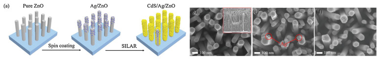
The sandwiched architecture of CdS/Ag/ZnO NRs was fabricated via a three-step process of hydrothermal growth of ZnO NRs, spin-coating for Ag NPs deposition and SILAR for CdS nanocrystallites coating, as schemed in Fig. 1a (Details can be found in Experimental section in Supporting information). In the hydrothermal step, ZnO NRs in hexagonal section shape were grown uniformly on FTO substrates, as shown in Fig. 1b, with diameter around 60~120 nm and length up to 3 μm. Through a simple spin-coating process, Ag NPs with approximate size of dozens of nanometers were deposited on the surface of ZnO NRs (Fig. 1c). The obtained Ag/ZnO film was then coated by CdS nanocrystallites via the SILAR process. As shown in Fig. 1d, CdS nanocrystallites were evenly dispersed on the surface of Ag/ZnO NRs, to form a sandwiched CdS/Ag/ZnO NR structure with rough surface. Given the almost complete coverage of the outmost CdS layer, Ag NPs could be hardly tracked in the CdS/Ag/ZnO NRs from SEM image (Fig. 1d).

|
Download:
|
| Fig. 1. (a) Scheme for the fabrication process of CdS/Ag/ZnO NRs on the FTO substrate. SEM images of (b) pure ZnO, (c) Ag/ZnO, (d) CdS/Ag/ZnO. | |
To see the shape and morphology of as-synthesized samples more clearly, TEM and HRTEM characterizations were further taken (Fig. 2). It can be clearly seen that ZnO NRs show a parallel fringe spacings of 0.26 nm (Fig. 2a), which is related to the (002) planes of wurtzite ZnO [29]. Through a spin-coating process, Ag NPs of ca. 20 nm in diameter were successfully deposited on the surface of ZnO NRs (Fig. S1 in Supporting information). The parallel fringe spacings of 0.236 nm further confirm the existence of metallic Ag (Fig. 2b, inset). As shown in Fig. S2 (Supporting information) and Fig. 2b, a ~20 nm thick layer of CdS nanocrystallites with average size of ~5 nm was uniformly deposited on the surface of ZnO NRs via SILAR process. The lattice spacings were measured to be 0.331 nm, which are consistent with the (002) plane of wurtzite CdS [30]. From the elemental mapping of sandwiched CdS/Ag/ZnO (Figs. 2c–f), one can easily observe that Ag NPs were embedded in the CdS layer, locating at the interface of ZnO NRs and CdS overlayer.

|
Download:
|
| Fig. 2. TEM and HRTEM images of (a) pure ZnO, (b) CdS/Ag/ZnO; (c–f) elemental mappings of CdS/Ag/ZnO. | |
The structures of all samples were characterized by X-ray diffraction (XRD). Fig. S3 (Supporting information) illustrates the XRD patterns of ZnO, Ag/ZnO, CdS/ZnO, and CdS/Ag/ZnO films. All the diffraction peaks can be well indexed to the standard diffraction patterns of wurtzite CdS and wurtzite ZnO [31, 32]. No XRD patterns of Ag NPs were detected, mainly due to the small size and low concentration of Ag NPs. To further investigate the crystal structure, all the samples were characterized by Raman spectra. As shown in Fig. 3a, one can see five obvious peaks. The two peaks located near 300 and 602 cm-1 were related to the active modes of LO and 2LO, respectively, confirming the wurtzite structure of the deposited CdS overlayer [33]. The other three peaks at 436, 580 and 980 cm-1 are the characteristics of wurtzite ZnO, corresponding to the E2 (high) vibrational, silent B1 (high), and 2TO (transverse-optical) modes, respectively [29, 34].

|
Download:
|
| Fig. 3. (a) Raman spectra of pure ZnO, Ag/ZnO, CdS/ZnO, and CdS/Ag/ZnO NRs; XPS spectra for pure ZnO, Ag/ZnO, CdS/ZnO, and CdS/Ag/ZnO NRs: (b) Zn 2p, (c) Ag 3d, (d) Cd 3d. | |
Chemical state and surface atomic compositions of the obtained films were confirmed by XPS analysis with results shown in Figs. 3b–d. The high resolution XPS spectra of Zn 2p of pure ZnO and CdS/ZnO samples depict two major peaks at 1021.6 eV and 1044.6 eV, corresponding to Zn 2p3/2 and Zn 2p1/2 [35], respectively. The Zn 2p positions of the Ag/ZnO and CdS/Ag/ZnO samples were shifted by about 0.4 eV towards lower binding energy, as compared with the corresponding value of pure ZnO (Fig. 3b). Meanwhile, the Ag 3d5/2 position of the Ag/ZnO sample (367.4 eV) (Fig. 3c) was shifted by about 0.8 eV towards lower binding energy compared with the corresponding value of pure metallic Ag (368.2 eV) [36]. These remarkable shifts of Zn 2p and Ag 3d binding energies suggest an interaction between Ag and ZnO nanocrystals at the microstructural level [37]. It is physically well known that when metal and semiconductor are brought together, Fermi levels will be realigned. In the case of Ag/ZnO, the corresponding Fermi levels of Ag and ZnO need to adjust to the same level, when they are contacting with each other. Therefore, some free electrons in Ag would transfer to ZnO, resulting in the higher valence of Ag and then the shift of the Ag 3d peak towards lower binding energy [38]. In comparison, the binding energy of Ag 3d for CdS/Ag/ZnO sample is 0.6 eV higher than that of Ag/ZnO sample, which is much closer to the corresponding value of pure metallic Ag. This shift might be caused by the electron transfer among the three components. The Cd 3d5/2 and Cd 3d3/2 peaks were found at the binding energy of 404.9 eV and 411.6 eV (Fig. 3d), respectively, evidencing the Cd2+ in CdS [39].
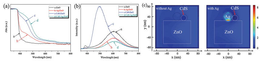
To investigate the optical characteristics of the as-fabricated films, the UV–vis absorption spectra and photoluminescence (PL) spectra were collected. As shown in Fig. 4a, the ZnO NRs show a strong absorption below 380 nm, which matches its band gap of 3.2 eV. After Ag NPs decoration, the obtained Ag/ZnO film shows optical absorption onset red shifted to ~660 nm, with an absorption shoulder at around 420 nm, which corresponds well to the LSPR absorption of Ag NPs [40]. It can be clearly seen that the absorption onset of ZnO NRs deposited with CdS nanocrystallites extends to 530 nm, which can be assigned to the characteristic absorption of CdS (Eg =2.4 eV). With both Ag NPs and CdS nanocrystallites deposited on ZnO NRs, the obtained CdS/Ag/ZnO film shows further enhanced optical absorption in visible light region, due to the synergistic effect of LSPR effect of Ag NPs and narrow band gap of CdS. PL spectra were collected to investigate the charge carrier transfer ability of the obtained films (Fig. 4b). The spectrum of pure ZnO consists of two emission components: a narrow UV peak at around 380 nm, which is assigned to near-band edge exciton emission, and a broad visible peak around 590 nm, which is correlated with deep level emission from intrinsic and extrinsic defects [41]. Compared with pure ZnO film, both the two PL peaks of Ag/ZnO film show intensities greatly decreased. The PRET enhanced charge carrier separation caused by Ag NPs loading might contribute to the UV emission depression [42], while the decrease in visible light peak intensity should be related to the passivation effect of Ag NPs which reduces the surface states or structural defects of ZnO [43, 44]. For the CdS/ZnO film, the decrease in both the UV and visible peak intensities could be traced to the promotion charge carrier separation due to the wellmatched band structures of CdS and ZnO. A new peak standing out at around 500 nm in the spectrum of CdS/ZnO can be assigned to the band gap transition of CdS nanocrystallites [37]. In the PL spectrum of CdS/Ag/ZnO film, the more attenuation in PL peak at around 380 nm and the PL quenching at around 500 nm indicate the more increased charge separation efficiency in CdS/Ag/ZnO due to the synergistic effect of PRET process of plasmonic Ag NPs and heterostructure configured by CdS and ZnO. The decreased PL peak at around 590 nm might be caused by the combined passivation effect of Ag NPs and CdS nanocrystallites. In order to more clearly identify the effect of Ag NPs in CdS/Ag/ZnO NRs on charge carrier transfer ability, we performed finite-difference time domain (FDTD) simulations to calculate the spatial distribution of electromagnetic field intensity of CdS/ZnO films with and without Ag NPs (Fig. 4c). It can be noted that the electromagnetic field density at the interface of Ag/ZnO and Ag/CdS in CdS/Ag/ZnO is much stronger than that of the CdS/ZnO interface without Ag NPs. This enhancement in electromagnetic field density could promote the charge carrier transfer from CdS nanocrystallites to Ag NPs and then from Ag NPs to ZnO NRs. As a result, the electron-hole pairs at the interface of CdS/ZnO are separated more efficiently, which will benefit the enhancement in PEC performance. The obtained optical properties and FDTD results indicate that the CdS/Ag/ZnO NRs present extended photo-response range, strong optical absorbance and excellent charge carrier transfer and separation due to the synergistic effects of Ag NPs and CdS nanocrystallites.

|
Download:
|
| Fig. 4. (a) UV–vis absorption spectra and (b) photoluminescence spectra of pure ZnO, Ag/ZnO, CdS/ZnO, and CdS/Ag/ZnO NRs; (c) Spatial distribution of electromagnetic field for CdS/ZnO and CdS/Ag/ZnO. | |
The PEC activity of the prepared CdS/Ag/ZnO sandwiched structure was investigated in detail as a photoanode under simulated solar light illumination. As shown in Fig. 5a, the photocurrent density of Ag/ZnO photoanode is slightly improved after Ag NPs loading, while the photocurrent density of CdS/ZnO photoanode is much higher than that of pure ZnO. Moreover, the photocurrent density of CdS/Ag/ZnO photoanode is significantly improved as compared to those of other three photoanodes. The photocurrent density of CdS/Ag/ZnO photoanode reaches 4.7 mA/cm2 at 1.6 V vs. RHE, which is around 8 times, 7.3 times and 1.7 times as high as that of pure ZnO, Ag/ZnO and CdS/ZnO photoanodes, respectively. This might be due to the synergistic effect of Ag NPs and CdS nanocrystallites. To further investigate the wavelength dependent photo-response, we performed the IPCE tests on all samples (Fig. 5b). The ZnO photoanode exhibits PEC activity only in the UV region, consisting with the optical absorption of ZnO limited in the UV region (Fig. 4a). The decoration of Ag NPs on ZnO NRs increased the IPCE values slightly in both UV and visible light region. The IPCE enhancement of Ag/ZnO photoanode in UV region can be assigned to the PRET effect of Ag NPs, which promotes the charge carrier separation, while enhancement in visible light region can be ascribed to the extended optical absorption due to the LSPR effect of Ag NPs, with hot electrons injected from Ag NPs to ZnO NRs via DET process. For the CdS/ZnO photoanode, the photo-response range of IPCE is extended to ca. 530 nm and the IPCE values are greatly enhanced, in accordance with the extended optical absorption region of CdS/ZnO. The CdS/Ag/ZnO photoanode exhibits PEC activity in the photo-response range as far as ~660 nm, consisting well with the optical absorption spectrum of CdS/Ag/ZnO. In the region of λ < 530 nm, the IPCE enhancement of CdS/Ag/ZnO photoanode as compared with CdS/ZnO photoanode should be related to the promoted charge carrier separation at the CdS/ZnO interface (Fig. 4b), as triggered by the strong electromagnetic density introduced by plasmonic Ag NPs (Fig. 4c). In addition, the IPCE enhancement of CdS/Ag/ZnO photoanode in photo-response region from 530 nm to 660 nm can be related to the extended optical absorption of Ag NPs and the DET process.

|
Download:
|
| Fig. 5. (a) Current-potential (I-V) curves of pure ZnO, Ag/ZnO, CdS/ZnO and CdS/Ag/ZnO NRs under solar simulator irradiation, (b) IPCE curves of pure ZnO, Ag/ZnO, CdS/ZnO and CdS/Ag/ZnO NRs. | |
Based on the previous analysis, the enhanced PEC activity of CdS/Ag/ZnO photoanode should be attributed to the synergistic effect of plasmonic Ag NPs and CdS nanocrystallites for the improved optical absorption in visible light as well as the promoted charge carrier separation efficiency. As indicated by the optical absorption spectra, ZnO could only be excited under UV light illumination (Fig. 6a). For Ag/ZnO NRs (Fig. 6b), Ag NPs could slightly increase PEC activity by (i) extending the optical absorption range through the LSPR effect, as indicated by the UV–vis spectra (Fig. 4a) and (ii) promoting charge carrier separation via PRET, as verified by PL spectra (Fig. 4b). For CdS/ ZnO NRs (Fig. 6c), CdS nanocrystallites could significantly expand the photo-response range to 530 nm for its narrow band gap (Fig. 4a) and enhance the charge carrier separation efficiency for the well-matched type Ⅱ band structure alignment between ZnO and CdS (Fig. 4b, Fig. S4 and Table S1 in Supporting information). Therefore, the PEC performance of CdS/ZnO photoanode was remarkably enhanced in UV and visible light region as compared with that of pure ZnO photoanode. The sandwiched CdS/Ag/ZnO photoanode displays significantly increased PEC performances in both UV and visible light region as compared with pure ZnO, Ag/ZnO and CdS/ZnO photoanodes, which can be ascribed to the synergistic effect of Ag NPs and CdS nanocrystallites in improving optical absorption property and enhancing charge carrier separation efficiency (Fig. 6d). On one hand, due to the LSPR effect of Ag NPs and narrow band gap of CdS, the photo-response range of CdS/Ag/ZnO could be effectively extended to ~660 nm. On the other hand, the type Ⅱ band structure alignment between CdS and ZnO facilitates the charge carrier separation. Moreover, the introduction of Ag NPs in the heterostructure accelerates the charge carrier separation at the interface of CdS and ZnO more efficiently due to the PRET effect of Ag NPs.

|
Download:
|
| Fig. 6. Schematics of charge carrier transfer processes in (a) ZnO, (b) Ag/ZnO, (c) CdS/ZnO, (d) CdS/Ag/ZnO. | |
In summary, CdS nanocrystallites sensitized ZnO NRs with plasmonic Ag NPs decoration was fabricated via a spin-coating and SILAR two-step process for PEC solar hydrogen generation. The obtained sandwiched CdS/Ag/ZnO NRs exhibited quite high PEC activity, with photocurrent density achieving 4.7 mA/cm2 at 1.6 V vs. RHE, which is 8 and 1.7 times as high as those of pure ZnO and CdS/ZnO NRs, respectively. Furthermore, with optical absorption onset extended to ~660 nm, the IPCE of CdS/Ag/ZnO photoanode reaches 23.1% and 9.8% at 400 nm and 500 nm, respectively. The PEC enhancement can be attributed to the one-dimensional ZnO NR structure maintained for superior charge transfer, and the extended visible-light absorption of CdS nanocrystallites. Moreover, the incorporated plasmonic Ag NPs could further promote the interfacial charge carrier transfer process and enhance the optical absorption ability, due to its excellent plasmon resonance effect. This study provides an effective strategy to design heterostructured photoelectrodes for efficient solar hydrogen conversion by synergistically extending visible light absorption and improving photogenerated charge carrier separation.
AcknowledgmentsThe authors gratefully acknowledge the financial support from the National Natural Science Foundation of China (No. 51672210) and the National Key Research and Development Program of China (No. 2018YFB1502003).
Appendix A. Supplementary dataSupplementary material related to this article can befound, in the online version, at doi:https://doi.org/10.1016/j.cclet.2019.07.020.
| [1] |
M. Grätzel, Nature 414 (2001) 338-344. DOI:10.1038/35104607 |
| [2] |
T. Hisatomi, J. Kubota, K. Domen, Chem. Soc. Rev. 43 (2014) 7520-7535. DOI:10.1039/C3CS60378D |
| [3] |
A. Fujishima, K. Honda, Nature 238 (1972) 37-38. DOI:10.1038/238037a0 |
| [4] |
F. Cao, J. Xiong, F. Wu, et al., ACS Appl. Mater. Interfaces 8 (2016) 12239-12245. DOI:10.1021/acsami.6b03842 |
| [5] |
H. Ma, W. Ma, J.F. Chen, et al., J. Am. Chem. Soc. 140 (2018) 5272-5279. DOI:10.1021/jacs.8b01623 |
| [6] |
H. Han, S. Kment, F. Karlicky, et al., Small 14 (2018) 1703860. DOI:10.1002/smll.201703860 |
| [7] |
X. Li, S. Liu, K. Fan, et al., Adv. Energy Mater. 8 (2018) 1800101. |
| [8] |
S. Hernández, V. Cauda, A. Chiodoni, et al., ACS Appl. Mater. Interfaces 6 (2014) 12153-12167. DOI:10.1021/am501379m |
| [9] |
Q. Li, X. Sun, K. Lozano, Y.B. Mao, J. Phys. Chem. C 118 (2014) 13467-13475. DOI:10.1021/jp503155c |
| [10] |
X. Zhang, Y. Liu, Z. Kang, ACS Appl. Mater. Interfaces 6 (2014) 4480-4489. DOI:10.1021/am500234v |
| [11] |
Y.K. Hsu, Y.C. Chen, Y.G. Lin, ACS Appl. Mater. Interfaces 7 (2015) 14157-14162. DOI:10.1021/acsami.5b03921 |
| [12] |
H.M. Chen, C.K. Chen, R.S. Liu, et al., Chem. Soc. Rev. 41 (2012) 5654-5671. DOI:10.1039/c2cs35019j |
| [13] |
J. Han, Z. Liu, K. Guo, et al., Appl. Catal. B-Environ. 179 (2015) 61-68. DOI:10.1016/j.apcatb.2015.05.008 |
| [14] |
C. Zhang, M. Shao, F. Ning, et al., Nano Energy 12 (2015) 231-239. DOI:10.1016/j.nanoen.2014.12.037 |
| [15] |
Y.F. Xu, H.S. Rao, X.D. Wang, et al., J. Mater. Chem. A 4 (2016) 5124-5129. DOI:10.1039/C5TA10563C |
| [16] |
L. Cai, F. Ren, M. Wang, et al., Int. J. Hydrogen Energy 40 (2015) 1394-1401. DOI:10.1016/j.ijhydene.2014.11.114 |
| [17] |
K. Zhao, X. Yan, Y. Gu, Y. Zhang, et al., Small 12 (2016) 245-251. DOI:10.1002/smll.201502042 |
| [18] |
S. Cao, X. Yan, Z. Kang, et al., Nano Energy 24 (2016) 25-31. DOI:10.1016/j.nanoen.2016.04.001 |
| [19] |
S. Wang, B. Zhu, M. Liu, et al., Appl. Catal. B-Environ. 243 (2019) 19-26. DOI:10.1016/j.apcatb.2018.10.019 |
| [20] |
Z. Bai, X. Yan, Y. Li, et al., Adv. Energy Mater. 6 (2016) 1501459. |
| [21] |
Z. Liu, W. Hou, P. Pavaskar, M. Aykol, S.B. Cronin, NanoLett. 11 (2011) 1111-1116. DOI:10.1021/nl104005n |
| [22] |
M. Wu, W.J. Chen, Y.H. Shen, et al., ACS Appl. Mater. Interfaces 6 (2014) 15052-15060. DOI:10.1021/am503044f |
| [23] |
S. Linic, P. Christopher, D.B. Ingram, Nat. Mater. 10 (2011) 911. DOI:10.1038/nmat3151 |
| [24] |
S.K. Cushing, J. Li, F. Meng, et al., J. Am. Chem. Soc. 134 (2012) 15033-15041. DOI:10.1021/ja305603t |
| [25] |
N. Wu, Nanoscale 10 (2018) 2679-2696. DOI:10.1039/C7NR08487K |
| [26] |
J. Li, S.K. Cushing, P. Zheng, et al., J. Am. Chem. Soc. 136 (2014) 8438-8443. DOI:10.1021/ja503508g |
| [27] |
W. Zhang, W. Wang, H. Shi, et al., Sol. Energy Mater. Sol. Cells 180 (2018) 25-33. DOI:10.1016/j.solmat.2018.02.020 |
| [28] |
J. Chen, M. Yu, Y. Wang, et al., Chin. Sci. Bull. 59 (2014) 2191-2198. |
| [29] |
M. Wang, F. Ren, G. Cai, et al., Nano Res. 7 (2013) 353-364. |
| [30] |
G. Wang, X. Yang, F. Qian, J.Z. Zhang, Y. Li, Nano Lett. 10 (2010) 1088-1092. DOI:10.1021/nl100250z |
| [31] |
C. Pacholski, A. Kornowski, H. Weller, Angew. Chem. Int. Ed. 41 (2002) 1188-1191. DOI:10.1002/1521-3773(20020402)41:7<1188::AID-ANIE1188>3.0.CO;2-5 |
| [32] |
J. Yu, J. Zhang, M. Jaroniec, Green Chem. 12 (2010) 1611-1614. DOI:10.1039/c0gc00236d |
| [33] |
Q. An, X. Meng, P. Sun, ACS Appl. Mater. Interfaces 7 (2015) 22941-22952. DOI:10.1021/acsami.5b06166 |
| [34] |
R. Cuscó, Alarcón-Lladó E., J. Ibáñez, et al., Phys. Rev. B 75 (2017) 165202. |
| [35] |
Y. Fang, Y. Xu, X. Li, Y. Ma, X. Wang, Angew. Chem. Int. Ed. 57 (2018) 9749-9753. DOI:10.1002/anie.201804530 |
| [36] |
D. Vidyasagar, S.G. Ghugal, A. Kulkarni, et al., Appl. Catal. B-Environ. 221 (2018) 339-348. DOI:10.1016/j.apcatb.2017.09.030 |
| [37] |
P. Bazant, I. Kuritka, L. Munster, L. Kalina, Cellulose 22 (2015) 1275-1293. DOI:10.1007/s10570-015-0561-y |
| [38] |
S. Chenakin, N. Kruse, J. Catal. 358 (2018) 224-236. DOI:10.1016/j.jcat.2017.12.010 |
| [39] |
J. Low, B. Dai, T. Tong, C. Jiang, J. Yu, Adv. Mater. 31 (2019) 1802981. DOI:10.1002/adma.201802981 |
| [40] |
J. Chen, S. Shen, P. Guo, et al., J. Mater. Res. 29 (2014) 64-70. DOI:10.1557/jmr.2013.200 |
| [41] |
S. Dellis, N. Kalfagiannis, S. Kassavetis, et al., J. Appl. Phys. 121 (2017) 103104. DOI:10.1063/1.4977954 |
| [42] |
S.R. Lingampalli, U.K. Gautam, C.N.R. Rao, Energy Environ. Sci. 6 (2013) 3589-3594. DOI:10.1039/c3ee42623h |
| [43] |
T. Wang, B. Jin, Z. Jiao, et al., J. Mater. Chem. A 2 (2014) 15553-15559. DOI:10.1039/C4TA02960G |
| [44] |
M. Wang, M. Wang, Y. Fu, S. Shen, Chin. Chem. Lett. 28 (2017) 2207-2211. DOI:10.1016/j.cclet.2017.11.037 |