 2019, Vol. 30


b Institute of Microstructure Technology, Karlsruhe Institute of Technology, Eggenstein-Leopoldshafen 76344, Germany;
c Light Technology Institute, Karlsruhe Institute of Technology, Karlsruhe 76131, Germany;
d Hubei Collaborative Innovation Center for Advanced Organic Chemical Materials, Ministry-of-Education Key Laboratory for the Green Preparation and Application of Functional Materials, Faculty of Materials Science and Engineering, Hubei University, Wuhan 430062, China
In the past few years, organic–inorganic hybrid perovskite solar cells (PSCs) have attracted considerable attention with sharply increasing power-conversion efficiencies (PCEs) exceeding 23% [1]. Many efforts have been reported for enhancing PECs via interface modification [2-4], improvements of device architecture [5, 6], control of morphology and crystal growth [7], etc. One of the essential requirements for achieving high-performance PSCs is to fabricate high-quality perovskite films. This can be achieved by systematically controlling their morphology and crystallization. Anti-solvent assisted treatment using such solvents as toluene, chlorobenzene (CB), diethyl ether or different acetate has been developed as a viable way of achieving this goal [8]. However, different solution methods and device configuration affects how effective anti-solvent assisted treatment can be in improving the morphology of the perovskite layer. On the other hand, using lead acetate (Pb(Ac)2) as lead source instead of lead iodide (PbI2) has been shown to be an efficient strategy to produce fully covered and ultrasmooth perovskite films via rapid removal of excess organic material and faster crystal growth [9]. To date, Pb(Ac)2 was employed as an additive in PbI2-derived precursor to form pinholefree perovskite films with large grains and low defect densities [10]. Furthermore, the additions of hypophosphorous acid (HPA) and dimethyl sulfoxide (DMSO) were used to improve the quality of Pb(Ac)2-based perovskite films [11, 12]. However, Pb(Ac)2-derived perovskite films assisted with anti-solvent treatment have rarely been reported.
In this study, we have implemented an anti-solvent process to produce highly homogeneous perovskite films based on lead acetate. It is known that the morphology of perovskite film can be easily affected by the surface uniformity of TiO2 film and different solution-processable methods. By exploring different solution methods (one-step and two-step solution-based deposition) and device architectures (planar and mesoporous PSC), we study the effect of anti-solvent treatment on the quality and morphology of these lead acetate derived perovskite cells. Our results show that anti-solvent treatment for a planar perovskite layer can result in larger grain size and improved surface morphology of the films leading to a 2% increase in PCE compared to the untreated films.
For the one-step solution method, the MAPbI3 precursor solution was generated by CH3NH3I (MAI, 99%, MaterWin) and Pb(Ac)2·3H2O (≥99.5%, SINOPHARM) mixture at a 3:1 molar ratio in anhydrous N, N-dimethylformamide (DMF, 99.8%, SigmaAldrich) to form final concentrations of ~30 wt%. The perovskite layer was prepared on top of the TiO2 film (cp-TiO2 or mp-TiO2 layers) by spin-coating at 2000 rpm for 30 s in the glovebox. For the anti-solvent assisted treatment, 100 μL CB (99.8%, Sigma-Aldrich) was slowly dripped onto the perovskite film after starting the perovskite spin-coating process. After that, the immediate perovskite films were left in the glass dish drying for 10 min and then annealed at 100 ℃ for 5 min. The two-step solution method is similar to the solution process by using PbI2 source. By using a 1 mol/L Pb(Ac)2·3H2O solution dissolved in DMF, the lead acetate film was deposited on top of the TiO2 film (cp-TiO2 or mp-TiO2 layers) by spin-coating at 2000 rpm for 30 s, and then annealed at 100 ℃ for 5 min. The transparent lead acetate film was immersed into a 10 mg/mL MAI solution dissolved in isopropanol (99.5%, Sigma-Aldrich), followed by annealing at 100 ℃ for 5 min.
FTO substrates (< 14 Ω/sq, Wuhan Jinge) were cleaned by acetone, ethanol, and deionized water, successively, and then were treated by oxygen plasma for 5 min. The cp-TiO2 film was deposited by direct-frequency magnetron sputtering (DFMS) onto the pre-cleaned FTO substrates, followed by annealing at 500 ℃ for 15 min. The mp-TiO2 film was deposited on top of the cp-TiO2 layer by spin-coating the TiO2 paste (Dysol 18NR-T) at 3000 rpm for 30 s, followed by annealing at 550 ℃ for 1 h. The perovskite layer was fabricated as described above. The perovskite films prepared by using one-step (two-step) solution method were termed 1-cp-MAPbI3 (2-cp-MAPbI3), 1-mp-MAPbI3 (2-mp-MAPbI3) for planar and mesoporous structures respectively. The CB processed films were termed 1-cp-MAPbI3 (+CB) and 2-cp-MAPbI3 (+CB). A spiro-OMeTAD (MaterWin) solution in chlorobenzene (99.8%, SIGMA-ALDRICH) containing additives of 4-tert-butylpyridine (TBP, 99%, MaterWin) and lithium bis(trifluoromethanesulfonyl)imide (Li-TFSI, 99%, MaterWin) was then deposited on the perovskite layer at 3000 rpm for 30 s. After storing overnight in the glovebox, Au film with 80-nm thickness was deposited by thermal evaporation to serve as the back contact for the solar cell.
The morphology of the perovskite films and the cross-section of whole cell were imaged via field-emission scanning electron microscopy (FE-SEM, Jeol JEM 6510 LV). The top views of TiO2 films were observed by atomic force microscopy (AFM, Nanoscope-Ⅲa). The X-ray diffraction (XRD) data of the perovskite and lead acetate films were collected with a Bruker-AXS D8 Advance. The absorption of the MAPbI3 and Pb(Ac)2 films were recorded by a UV-vis spectrophotometry (UV-3600, Shimadzu). The current density–voltage (J–V) curves were measured by using a solar simulator (Oriel, model 91192-1000) and a source meter (Keithley 2400, USA) under simulated AM 1.5 sunlight of 100 mW/cm2 irradiance.
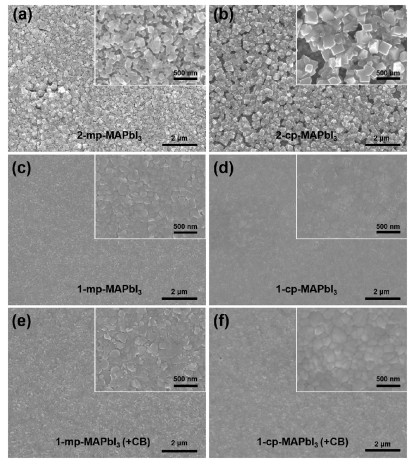
Fig. 1 shows the morphologies of different perovskite layers. For two-step spin-coated perovskite layers, the films (Figs. 1a and b) are covered with a large number of cubic nanocrystals along with obvious cracks, indicating relatively low surface coverage on FTO substrates. These disrupted films come from the limited solubility of lead acetate trihydrate in DMF mainly due to the polymeric nature with chelated bridging acetate groups [13, 14], as well as the rapid nucleation and crystallization onto Pb(Ac)2 films during the annealing process, which cannot obtain continuous and uniform films. In contrast, one-step spin-coated perovskite films exhibited good uniformity without any obvious nanopinholes (Figs. 1c and d), especially in the planar configuration (1-cp-MAPbI3, Fig. 1d) with smooth andhomogeneous film. The planar perovskite film treated with CB (1-cp-MAPbI3 (+CB), as shown in Fig. 1f, achieved grain growth (up to ~300 nm) and morphology improvement compared to untreated (Fig. 1d), while the mesoporous perovskite films have no significant changes in morphologies without (Fig. 1c) and with CB treatment (Fig. 1e). These results suggest that perovskite morphologies may rely on morphologies of planar or mesoporous TiO2 layers.

|
Download:
|
| Fig. 1. Top-view FE-SEM topographies of pristine perovskite layers: (a) 2-mpMAPbI3, (b) 2-cp-MAPbI3, (c) 1-mp-MAPbI3, (d) 1-cp-MAPbI3, (e) 1-mp-MAPbI3 (+CB), (f) 1-cp-MAPbI3 (+CB). The perovskite films of (e) and (f) were treated with CB. The scale bars on the images and the insets showing higher resolution are 2 μm and 500 nm, respectively. | |
XRD patterns of different perovskite and Pb(Ac)2 films are shown in Fig. 2a. The perovskite films fabricated by one-step solution method invariably show a high degree of orientation in their crystal structure. It is evident that the perovskite film prepared by two-step solution deposition shows a diffraction feature at 9.06° associated with Pb(Ac)2, suggesting incomplete consummation of Pb(Ac)2 during soaking process. In the UV–vis absorption spectra of different perovskite films (Fig. 2b), we observe similar absorption edges at ~775 nm for one-step deposited samples, while a ~5-nm red shift in the absorption for two-step deposited perovskite films can be observed. These different optical behaviors are associated with the size and shape of the perovskite crystals and the presence of Pb(Ac)2/CH3NH3PbI3 heterostructures [9, 14, 15]. The light absorption of the perovskite films prepared using two-step solution method significantly improved over a wide wavelength range of 420–775 nm compared with that of one-step deposited films. This could attribute to enhancement in light scattering caused by rough surfaces [14] and the residual Pb(Ac)2 within the two-step deposited perovskite films, which are consistent with the SEM images and detected Pb(Ac)2 feature in the XRD patterns.

|
Download:
|
| Fig. 2. (a) XRD patterns of Pb(Ac)2 and different annealed perovskite films. Peaks marked with* are assigned to the traces of FTO. (b) UV - vis absorption spectra of Pb (Ac)2 and different perovskite films. (c) Schematic structure and (d) cross-sectional FE-SEM image of the mesoporous PSCs. The scale bar is 500 nm. (e) J–V curves of the best-performing device measured under simulated AM 1.5 sunlight of 100 mW/cm2 irradiance. (f) Histogram of PCEs for the 1-cp-MApbI3 and 1-cp-MApbI3 (+CB) PSCs based on 24 devices from 4 batches. | |
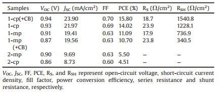
The typical mesoporous PSC with the architecture of FTO/cp-TiO2/mp-TiO2/Perovskite/Spiro-OMeTAD/Au is shown in Fig. 2c. The total thickness of mp-TiO2 and perovskite layer in mesoporous configuration is ~500 nm, while the thickness of perovskite layer in planar structure is ~350 nm (Fig. 2d, Figs. S1 and S2 in Supporting information). Fig. 2e gives the best performance of PSCs fabricated from different methods and configurations and Table 1 summarizes the corresponding photovoltaic performances. The two-step deposited devices show poor PCEs around 5% attributed to the lower short-circuit current density (JSC) below 10 mA/cm2. As we know, it is vital to minimize nonradiative recombination by controlling the grains and boundaries of the perovskite film [13, 16, 17]. The inferior JSC of two-step deposited perovskites correlates the morphological irregularities. In comparison, the one-step deposited devices show better performances, especially in the planar devices. Remarkably, the 1-cp(+CB) device fabricated with CB treated perovskite film achieved the best PCE of 15.80%, which is mainly attributed to the increase in JSC from 21.97 mA/cm2 to 23.90 mA/cm2, decrease in series resistance (RS) from 23.9 Ω/cm2 to 18.7 Ω/cm2, and increase in shunt resistance (RSH) from 1228.1 Ω/cm2 to 1540.8 Ω/cm2.
|
|
Table 1 Summarized photovoltaic parameters of PSCs based on different solution methods and device architectures. |
However, the mesoporous device with CB treated perovskite film had no significant improvement in device performance, which is due to the relatively lower JSC and RSH· Fig. 2f shows the histogram of PCEs in 24 PSCs with and without the CB treatment, which confirms that the introduction of the CB treatment leads to significant improvement in PCE and repeatability within the PSCs.
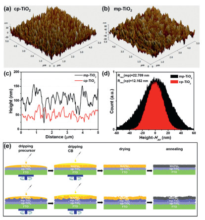
In order to explore the effects of morphologies of TiO2 layers on the device performances, AFM was performed on planar and mesoporous TiO2 thin films. As shown in Figs. 3a-d, the root-mean-square roughness (Rrms) of the cp-TiO2 and mp-TiO2 layers were calculated to be 12.162 nm and 22.709 nm, respectively, indicating that cp-TiO2 layer has a smoother surface than mp-TiO2 layer. It has been reported that the bumpy TiO2 layer affected the surface uniformity of perovskite film [18]. As an example, Fig. 3e gives the schematic of the stages in fabrication of MAPbI3 based on cp-TiO2 and mp-TiO2 layers. During the initial stages of precursor coating, the solvent gradually evaporated but the excess organic component was entrapped within the film, thus retarding full crystallization into the perovskite [9]. During antisolvent process, CB washing can speed up the nucleation and crystal growth, thereby providing enhanced homogeneous perovskite film [19, 20]. In the drying and annealing stages, the excess organic component was conducive to the formation of a uniform perovskite film, and the residual CB began to leave until the film was heated at 100 ℃ [9, 21]. As a whole, an uneven mpTiO2 film with a roughness surface would not lead to the formation of a smooth perovskite film.

|
Download:
|
| Fig. 3. Surface morphologies from AFM 3D views of (a) cp-TiO2 and (b) mp-TiO2 films. (c) Representative line segments and (d) height distributions around average heights (HAV) of different TiO2 films derived from AFM characterization. (e) Illustration of the stages in the fabrication of MAPbI3 thin films. | |
In summary, we have implemented an efficient strategy to produce fully covered and homogeneous perovskite films via antisolvent treatment process while using Pb(Ac)2 as Pb source. We also show that the morphology of perovskite film can be easily regulated by the surface uniformity of TiO2 films. Obtained results indicate that the planar devices fabricated by one-step solution method achieved smooth and pinhole-free films, and CB treatment further promoted the film quality and enlarged the grain sizes. The best device (1-cp(+CB)) achieved a PCE of 15.80%, which is mainly attributed to the high JSC (up to 23.90 mA/cm2), low RS and high RSH. Hence, this study demonstrates the possibility of using antisolvent treatment to improve the morphology of Pb(Ac)2-derived perovskite which provides a feasible pathway to improve the efficiency of PHJ PSCs.
AcknowledgmentsThis work was supported by the National Natural Science Foundation of China (NSFC, Nos. 51572072 and 21402045), Wuhan Science and Technology Bureau of Hubei Province of China (No. 2013010602010209), Educational Commission of Hubei Province of China (No. D20141006) and Department of Science & Technology of Hubei Province of China (No. 2015CFA118).
Appendix A. Supplementary dataSupplementary material related to this article can be found, in the online version, at doi:https://doi.org/10.1016/j.cclet.2019.03.006.
| [1] |
Best Research-Cell Efficiencies. https://www.nrel.gov/pv/assets/pdfs/pvefficiency-chart.20181214.pdf(Accessed December 2018).
|
| [2] |
X. Zeng, T. Zhou, C. Leng, et al., J. Mater. Chem. A 5 (2017) 17499-17505. DOI:10.1039/C7TA00203C |
| [3] |
M. Wang, Z. Zang, B. Yang, et al., Sol. Energy Mater. Sol. Cells 185 (2018) 117-123. DOI:10.1016/j.solmat.2018.05.025 |
| [4] |
T. Zhou, M. Wang, Z. Zang, X. Tang, L. Fang, Sol. Energy Mater. Sol. Cells 191 (2019) 33-38. DOI:10.1016/j.solmat.2018.10.021 |
| [5] |
M.M. Lee, J. Teuscher, T. Miyasaka, T.N. Murakami, H.J. Snaith, Science 338 (2012) 643-647. DOI:10.1126/science.1228604 |
| [6] |
M. Liu, M.B. Johnston, H.J. Snaith, Nature 501 (2013) 395-398. DOI:10.1038/nature12509 |
| [7] |
W. Nie, H. Tsai, R. Asadpour, et al., Science 347 (2015) 522-525. DOI:10.1126/science.aaa0472 |
| [8] |
F. Yang, G. Kapil, P. Zhang, et al., ACS Appl. Mater. Interfaces 10 (2018) 16482-16489. DOI:10.1021/acsami.8b02554 |
| [9] |
W. Zhang, M. Saliba, D.T. Moore, et al., Nat. Commun. 6 (2015) 6142. DOI:10.1038/ncomms7142 |
| [10] |
G. Tang, P. You, Q. Tai, R. Wu, F. Yan, Sol. RRL 2 (2018) 1800066. DOI:10.1002/solr.v2.6 |
| [11] |
W. Zhang, S. Pathak, N. Sakai, et al., Nat. Commun. 6 (2015) 10030. DOI:10.1038/ncomms10030 |
| [12] |
Y. Liu, Z. Liu, E.C. Lee, J. Mater. Chem. C 6 (2018) 6705-6713. DOI:10.1039/C8TC01570H |
| [13] |
J.T. Lim, J.C. Lee, W.I. Lee, I.M. Lee, Bull. Korean Chem. Soc. 20 (1999) 355-361. |
| [14] |
M. Sima, E. Vasile, M. Sima, Mater. Res. Bull. 89 (2017) 89-96. DOI:10.1016/j.materresbull.2017.01.031 |
| [15] |
S. Yang, Y.C. Zheng, Y. Hou, et al., Chem. Mater. 26 (2014) 6705-6710. DOI:10.1021/cm5028817 |
| [16] |
S.H. Im, I.H. Jang, N. Pellet, M. Gratzel, N.G. Park, Nat. Nanotechnol. 9 (2014) 927-932. DOI:10.1038/nnano.2014.181 |
| [17] |
Z. Xiao, Q. Dong, C. Bi, et al., Adv. Mater. 26 (2014) 6503-6509. DOI:10.1002/adma.201401685 |
| [18] |
M. Kong, H. Hu, L. Wan, et al., RSC Adv. 7 (2017) 35549-35557. DOI:10.1039/C7RA04924B |
| [19] |
M. Zhang, Z. Wang, B. Zhou, et al., Sol. RRL 2 (2018) 1700213. DOI:10.1002/solr.v2.2 |
| [20] |
D. Prochowicz, M.M. Tavakoli, A. Solanki, et al., J. Mater. Chem. A 6 (2018) 14307-14314. DOI:10.1039/C8TA03782E |
| [21] |
Y. Wang, J. Wu, P. Zhang, et al., Nano Energy 39 (2017) 616-625. DOI:10.1016/j.nanoen.2017.07.046 |