 2019, Vol. 30


b Department of Physics, University of Science and Technology of China, Hefei 230026, China;
c Key Laboratory of Flexible Electronics (KLOFE) & Institute of Advanced Materials (IAM), Jiangsu National Synergetic Innovation Center for Advanced Materials (SICAM), Nanjing Tech University, Nanjing 211816, China
Cu nanostructures have attracted much attention due to their applications in electronics, optics and catalysis [1-3]. The properties of Cu nanostructures depend on their size and morphology [4-6]. In particular, the anisotropic Cu nanostructures such as nanowires (NWs) and nanosheets (NSs) have unique electrical and catalytic properties which attributed to their size effect and facet effect [7-10]. For examples, Cu NWs with the average diameter of 17.5 nm, which among the superior performing substitute for ITO [11]. However, it is difficult to synthesize anistropic Cu nanostructures with diameter less than 10 nm, which limit their futher application.
Moreover, many efforts have been made to fabricate Cu encapsulated core-shell nanostructures to improve their stability [12-18] and expand their applications in device [19] and catalysis [20]. For example, Cu nanoparticles coateded with MOF-5 exhibit prominent catalytic activity and stability for methanol synthesis [21]. Furthermore, the core-shell structures with metal encapsulated by metal-organic frameworks (MOFs) have been expounded to be promising in memory device due to the insulation of MOFs as well as the conductivity enhancement from the metal addition [22]. Therefore, it is desired to synthesize size-tunable anistropic Cu@Cu-BTC nanostructure, which might have the possibility for application in memory device due to the high conductivity and low prize of Cu.
Herein, we reported the formation of Cu@Cu-BTC core-shell nanosheets through a mild etching approach by using 1, 3, 5- benzenetricarboxylic acid. The thickness of the Cu NSs could be tuned from dozens of nanometers to several nanometers by controlling the in situ growth of Cu-BTC which combined the slow oxidation and the Cu-BTC formation. Furthermore, the memory device with the configuration of glass/ITO/Cu@Cu-BTC NSs/m-PEDOT:PSS was demonstrated to have the WORM behavior and the high ION/IOFF ratio (>2.7 × 10³).
In a typical synthesis, Cu NSs were used as a seed to obtain the Cu@Cu-BTC core-shell NSs. The Cu NSs were obtained as reported [23] by heating the mixture (0.15 mmol Cu(OAc)2, 297 mg PVP, 15 mL DMF solution, 90 mL hydrated hydrazine) from 40 ℃ to 60 ℃ for 3 min and kept for 15 min. Then, the separated and purified products together with 1, 3, 5-benzenetricarboxylic acid (H3BTC, 8 mg) were dissolved in 10 mL ethanol solution. The mixture was dispersed under magnetic stirring at room tempreture in a glass bottle with 20 mL volume. The Cu@Cu-BTC core-shell NSs and pure Cu-BTC NSs were obtained after reaction time of 1 h and 8 h, respectively (Fig. 1).

|
Download:
|
| Fig. 1. Schematic illustration for the formation of the Cu@Cu-BTC NSs. | |
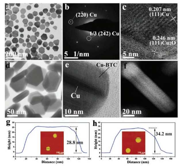
The obtained hexagon Cu NSs with diameter of about 100 nm were confirmed by the transmission electron microscopy (TEM) image (Fig. 2a). Selected-area electron diffraction pattern shows the fcc phase of Cu and the [111] incident direction of electron beam (Fig. 2b). The 1/3(422) reflections were found and attributed to the multiple stacking faults at {111} planes. The high resolution transmission electron microscopy (HRTEM) image (Fig. 2c) shows that the crystal structure, with the lattice fringes of 0.207 nm, is corresponding to the {111} plane of Cu. Cu2O structures with the lattice fringes of 0.246 nm were observed and attributed to the slight oxidation on the surface of Cu NSs.

|
Download:
|
| Fig. 2. (a) TEM image, (b) selected-area electron diffraction pattern and (c) HRTEM image of Cu NSs. (d) TEM image, (e) HRTEM image and (f) HAADF-HRTEM image of the Cu@Cu-BTC NSs. AFM phase image (inset) and the corresponding height distribution of (g) Cu NSs and (h) Cu@Cu-BTC NSs. | |
As shown in the Figs. 2d and e, the obtained Cu@Cu-BTC NSs presented typical core-shell structures which were revealed by the obvious difference in contrast. The thin Cu NS with the thickness of sub-10 nm was obtained as the core of the Cu@Cu-BTC core-shell structure Figs. 2e and f). The atomic force microscopy (AFM) images and corresponding height distributions show that the height of Cu NSs and Cu@Cu-BTC NSs (1 h) are 28.8 nm and 34.2 nm, respectively, revealing the increase of height of the NSs along with the Cu-BTC coating Figs. 2g–h).
To confirm the formation mechanism of the Cu@Cu-BTC NSs, a time-dependent reaction process was investigated. The mild etching process was confirmed by the TEM images of Cu@Cu-BTC NSs which show that the thickness of Cu NSs decreased from dozens of nanometers to sub-10 nm along with the reaction time changing from 10 min to 3 h (Fig. S1 in Supporting information). The as-prepared NSs after reaction time of 8 h were typical Cu-BTC structures which confirmed by TEM image and XRD pattern (Fig. S2 in Supporting information). Particularly, the strategy could be applies to Cu NWs as well which confirmed by the TEM images (Fig. S3 in Supporting information).
Fig. 3a displays the X-ray diffraction (XRD) pattern of the Cu@Cu-BTC NSs after the reaction time of 1 h. Three pronounced reflection peaks appear at 2θ = 43.30°, 50.43°, and 74.13°, corresponding to the fcc Cu(111), (200), and (220) reflections, respectively. The other reflections with weak intensity appear in the range of 5°–40°. As shown in the amplified XRD pattern inset Fig. 3a, the positions of peaks agree with the simulated Cu3BTC2 and Cu(HBTC)(H2O)3 (Fig. S4 in Supporting information), which reveals that the Cu@Cu-BTC NSs are composed of fcc Cu and Cu-BTC. The formation of Cu(HBTC)(H2O)3 might be attributed to the unsaturated coordination caused by the different concentration of Cu ions.

|
Download:
|
| Fig. 3. (a) XRD patterns of the Cu@Cu-BTC NSs and magnified XRD patterns of the Cu@Cu-BTC NSs from 5° to 40° (inset). (b) Cu 2p XPS spectra of the Cu NSs (upper) and the Cu@Cu-BTC NSs (bottom). | |
The X-ray photoelectron spectroscopy (XPS) spectra of Cu 2p was measured with photon energies of 1486.6 eV. As shown in Fig. 3b, peaks at 952.5 and 932.5 eV can be assigned to Cu 2p1/2 and Cu 2p3/2 of the metallic Cu0, respectively. Additionally, The peaks at 953.7 and 933.3 eV are associated with Cu2+ 2p1/2 and Cu2+ 2p3/2. The Cu+ 2p signals overlap with the Cu2+ 2p signals around 953.7 eV and 933.3 eV, respectively, and the component of Cu could be obtained by the spectrum decomposition. The peak areas were calibrated by the beam flux and photoionization cross-section at the corresponding photon energy. As shown in Fig. 3b, the decrease of Cu0 content and the increase of Cu2+(Cu+) content after reaction of 1 h, illustrating the oxidation of Cu on the surface of NSs along with the formation of Cu-BTC.
On the other hand, the shell of the NS was confirmed to be Cu-BTC by the thermogravimetric analysis (TGA), in which the Cu@Cu-BTC NS have the same thermal decomposition temperature with the Cu-BTC at 350 ℃ (Fig. S5 in Supporting information). Moreover, in the UV–vis spectra of the Cu NSs and Cu@Cu-BTC NSs (Fig. S6 in Supporting information), the sharp band and weak band appear at 605 nm and 450 nm, respectively, as expected to be the in-plane and out-of-plane plasmon modes. The intensity of the band evidently decrease when the Cu NSs transformed to the Cu@Cu-BTC NSs, which in agreement with the coating process of Cu-BTC.
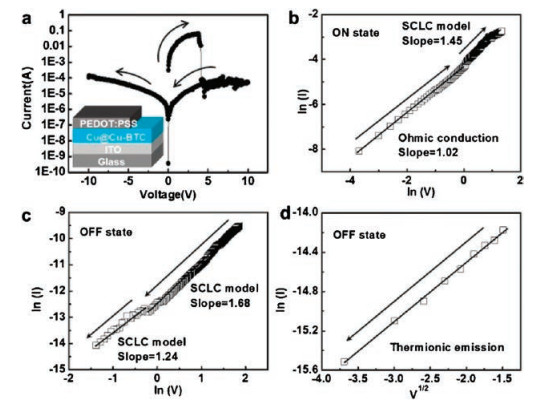
Previous studies have demonstrated that the hybridization of 2D nanomaterials has led to the enhanced performance in various applications [24]. As a proof-of-concept demonstration, the electronic property and switching effect of the memory device with the configuration of Glass/ITO/Cu@Cu-BTC/m-PEDOT:PSS was investigated by current-voltage (I-V) characteristics. As shown in Fig. 4a, the device exhibited a low resistance state (LRS) at voltage below ~4 V. This state could be considered as the ON state of the memory. With the increase of applied voltage, the current decreased from ~10-1 A to ~10-5 A, indicating the device was transferred to a high resistance state (HRS, defined as the OFF state). This electrical transition from a LRS to a HRS can be considered as the "writing" operation in data storage. After the writing process, the current of device remained low during the subsequent voltage sweeps, indicating a nonvolatile write-onceread-many times (WORM) memory effect. The WORM behavior means that the stored data could not be erased once it had been written, which showed potential applications in security and data protection [25]. Moreover, the high ION/IOFF ratio (>2.7 × 10³) is promising to realize a lower data misreading probability in such devices.

|
Download:
|
| Fig. 4. (a) Schematic and I-V characteristics of the fabricated Cu@Cu-BTC NSs based memory device. Experimental data and fitted lines of the I-V curves of (b) the low resistance state and (c, d) the high resistance state. | |
To understand the carrier transport mechanism of the Cu@Cu-BTC NSs based memory device, the experimental data and fitted I-V curves of the ON and OFF state were analyzed by using three different models [26], which include Ohmic conduction model, space charge limited current (SCLC) conduction model, and thermal emission model (Figs. 4b–d). In the ON state, the plot of ln(I) vs. ln(V) from 0 to 4 V shows two regions with two slope values of 1.02 and 1.45, respectively, indicating the electrical conduction is governed by the Ohmic law and followed by a subsequent SCLC transport (Fig. 4b). With a further increase in the bias, the slope values in the OFF state are 1.68 and 1.24, respectively, indicating both of the two regions are the SCLC model (Fig. 4c). In the later OFF state, the plot of ln(I) vs. V1/2 can be fitted to a straight lines (Fig. 4d), suggesting that the conduction mechanism in this region probably arises from the thermionic emission.
In summary, we reported the preparation of the Cu@Cu-BTC NSs by controlling the growth of Cu-BTC along with the oxidation on the surface of Cu NSs. This unique strategy can be extended to synthesize 1D Cu@Cu-BTC NWs. The ultrathin Cu NSs with the diameter of sub-10 nm could be observed after the mild etching through the formation of Cu-BTC. Moreover, the obtained Cu@Cu-BTC NSs can be applied as the effective material to a memory device with the typical WORM switching behaviour. It is expected that these unique nanosheets may also have prospects in catalysis reaction and energy storage.
AcknowledgmentsThis work was supported by the National Key R & D Program of China (No. 2017YFA0700104), National Natural Science Foundation of China (Nos. 21571169, 21871238), Fundamental Research Funds for the Central Universities (No. WK2060190081), Youth Innovation Promotion Association of the Chinese Academy of Sciences (No. 2018494) and Young Elite Scientists Sponsorship Program by CAST (No. 2016QNRC001).
Appendix A. Supplementary dataSupplementary material related to this article can befound, in the online version, at doi:https://doi.org/10.1016/j.cclet.2018.11.008.
| [1] |
M.B. Gawande, A. Goswami, F.X. Felpin, et al., Chem. Rev. 116 (2016) 3722-3811. DOI:10.1021/acs.chemrev.5b00482 |
| [2] |
D. Zhao, L. Xu, Y. Shang, X. Li, L. Guo, Nano Res. 11 (2018) 4836-4845. DOI:10.1007/s12274-018-2072-2 |
| [3] |
S. Han, S. Hong, J. Ham, et al., Adv. Mater. 26 (2014) 5808-5814. DOI:10.1002/adma.v26.33 |
| [4] |
R. Reske, H. Mistry, F. Behafarid, B.R. Cuenya, P. Strasser, J. Am. Chem. Soc. 136 (2014) 6978-6986. DOI:10.1021/ja500328k |
| [5] |
W.H. Ke, C.F. Hsia, Y.J. Chen, M.H. Huang, Small 12 (2016) 3530-3534. DOI:10.1002/smll.201600064 |
| [6] |
P. Gao, H. Ma, Q. Wu, et al., J. Phys. Chem. C 120 (2016) 17613-17619. DOI:10.1021/acs.jpcc.6b05712 |
| [7] |
Z. Niu, F. Cui, Y. Yu, et al., J. Am. Chem. Soc. 139 (2017) 7348-7354. DOI:10.1021/jacs.7b02884 |
| [8] |
S. Jeong, K. Woo, D. Kim, et al., Adv. Funct. Mater. 18 (2008) 679-686. DOI:10.1002/(ISSN)1616-3028 |
| [9] |
B. Xiao, Z. Niu, Y.G. Wang, et al., J. Am. Chem. Soc. 137 (2015) 3791-3794. DOI:10.1021/jacs.5b01391 |
| [10] |
L. Dai, Q. Qin, P. Wang, et al., Sci. Adv. 3 (2017) e1701069. DOI:10.1126/sciadv.1701069 |
| [11] |
F. Cui, Y. Yu, L. Dou, et al., Nano Lett. 15 (2015) 7610-7615. DOI:10.1021/acs.nanolett.5b03422 |
| [12] |
Q. Yao, Z.H. Lu, Z. Zhang, X. Chen, Y. Lan, Sci. Rep. 4 (2014) 7597. DOI:10.1038/srep07597 |
| [13] |
H. Xu, H. Wang, C. Wu, et al., Nanoscale 7 (2015) 10613-10621. DOI:10.1039/C5NR01711D |
| [14] |
Y. Ahn, Y. Jeong, D. Lee, Y. Lee, ACS Nano 9 (2015) 3125-3133. DOI:10.1021/acsnano.5b00053 |
| [15] |
Q. Li, J. Fu, W. Zhu, et al., J. Am. Chem. Soc. 139 (2017) 4290-4293. DOI:10.1021/jacs.7b00261 |
| [16] |
D. Liu, B. Wu, S. Mubeen, et al., ChemNanoMat 4 (2018) 914-918. DOI:10.1002/cnma.v4.9 |
| [17] |
L. Dou, F. Cui, Y. Yu, et al., ACS Nano 10 (2016) 2600-2606. DOI:10.1021/acsnano.5b07651 |
| [18] |
X.M. Liao, V. Pitchon, P.H. Cuong, W. Chu, V. Caps, Chin. Chem. Lett. 28 (2017) 293-296. DOI:10.1016/j.cclet.2016.06.043 |
| [19] |
T. Ghodselahi, H. Zahrabi, M.H. Saani, M.A. Vesaghi, J. Phys. Chem. C 115 (2011) 22126-22130. DOI:10.1021/jp204020j |
| [20] |
Y. Liu, Z. Tang, Adv. Mater. 25 (2013) 5819-5825. DOI:10.1002/adma.v25.40 |
| [21] |
M. Müller, S. Hermes, K. Kähler, et al., Chem. Mater. 20 (2008) 4576-4587. DOI:10.1021/cm703339h |
| [22] |
X. Huang, B. Zheng, Z. Liu, et al., ACS Nano 8 (2014) 8695-8701. DOI:10.1021/nn503834u |
| [23] |
I. Pastoriza-Santos, A. Sanchez-Iglesias, B. Rodriguez-Gonzalez, L.M. LizMarzan, Small 5 (2009) 440-443. DOI:10.1002/smll.v5:4 |
| [24] |
V. Stavila, A.A. Talin, M.D. Allendorf, Chem. Soc. Rev. 43 (2014) 5994-6010. DOI:10.1039/C4CS00096J |
| [25] |
J. Liu, Z. Yin, X. Cao, et al., Adv. Mater. 25 (2012) 233-238. DOI:10.1002/adma.201203349 |
| [26] |
Q.D. Ling, D.J. Liaw, C. Zhu, et al., Prog. Polym. Sci. 33 (2008) 917-978. DOI:10.1016/j.progpolymsci.2008.08.001 |