 2019, Vol. 30


Self-healing materials have attracted much attention owing to the ability to restore their properties when encountering destruction, similar to most natural biomaterials [1-3]. According to different self-healing principles, the self-healing materials are classified into 'intrinsic' and 'extrinsic' self-healing materials [4]. The former is designed based on reversible bonds including noncovalent or dynamic covalent bonds, which can be healed repeatedly [5-7]. The latter is based on external healing components like nanocapsules [8-10]. Compared with covalent bond, hydrogen bond that the association or dissociation occurs spontaneously at ambient conditions offers promising chances for developing intrinsic self-healing materials. Hydrogen-bond-based self-healing polymer (HSP) is an intensively researched selfhealing material which is developed by Leibler and coworkers [11]. It often combines with conducting materials for applications in electronic skin [12], supercapacitor [13], lithium-ion batteries [14, 15], thermal sensor [16]. However, these materials or devices are mainly based on self-healing process in three-dimension (3D). The research of the self-healing process of HSP polymer at the twodimensional (2D) space is still lacking.
2D materials have a structure with an atomic/molecular scale thickness while the lateral dimensions is several orders of magnitude larger than the thickness [17]. The 2D geometry endows them with unique properties like excellent flexibility, large surface area, electron confinement effect, high transparency, resulting in potential applications in electronics, photonics, energy storage, etc. Some pioneers have researched self-healing behaviour of the organic thin films. For instance, Zhang et al. observed selfhealing behaviour of coronene/1, 2, 4, 5-tetracyanobenzene cocrystal thin-film in a thermo-mechanically responsive process during reversible phase transition [18]. Seggern et al. found that the pentacene thin-film has a self-healing phenomena of the electrical property [19]. 2D self-healing materials have great potential for application in dielectric layer, lubricating layer, corrosion inhibitors and nanolithography applications, etc. However, a clear understanding of the 2D healing process is still absent. Study of the self-healing process at the 2D limit can enhance the comprehension of self-healing mechanism and promote the development of 2D functional self-healing materials. Herein, we prepare 2D HSP film by a simple one-step interfacial self-assembly method for the first time and explore the self-healing process at the 2D limit. Temperature, molecule-substrate interaction and the substrate roughness are major factors to influence the healing process. The HSP film can be reversibly healed for at least three times. After modifying the SiO2 dielectric with monolayer HSP film, the mobility of copper phthalocyanine (CuPc) field effect transistors (FETs) is improved owing to the smooth dielectric surface with self-healing property.
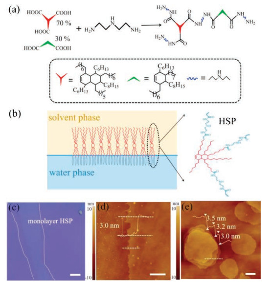
Before preparing 2D self-healing film, HSP was synthesized by modified Leibler's method [20]. Briefly, 20.3 g of fatty acid (Fig. 1a, 70 wt% triacids and 30 wt% diacids, Demand Chemical Co., Ltd. Shanghai) was reacted with 8 g of diethylenetriamine (SigmaAldrich) at 160 ℃ for 24 h under argon atmosphere and intensive magnetic stirring. Then the product was dissolved in 100 mL of chloroform by stirring and washed with 100 mL of deionized water and 50 mL of methanol, followed by removal of the residual chloroform by rotary evaporation. To remove chloroform completely, the product was put in vacuum oven at 70 ℃ overnight. The purified product was dissolved in chloroform to prepare different concentration solutions (0.8 mg/mL, 2 mg/mL, 3 mg/mL, 4 mg/mL). There were two methods to prepare monolayer HSP film. The first was spin-coating. 0.8 mg/mL HSP solution was spin-coated on different substrates at 3000 rpm for 30 s. The monolayer HSP film on hexagonal boron nitride (h-BN) and mica substrates was prepared by this method. The second utilized CHCl3/H2O interface. 20 mL of 4 mg/mL HSP/CHCl3 solution was dropped onto water surface, after 10 min to evaporate the solvent, a substrate was placed in the water to gently lift the film. Before usage, the SiO2/Si needed be modified by hydrophilic treatment. The SiO2/Si was immersed in H2SO4/H2O2 (v/v = 3:1) at 80 ℃ for 30 min, washed with deionized water for three times, and dried using nitrogen gas gun. Graphene was mechanical exfoliated from Natural Kish Graphite (Grade 300). The SiO2/Si was modified by octadecyltrichlorosilane (OTS) in vacuum oven and washed by dimethylbenzene for three times. All HSP films were annealed in oven at 70 ℃ overnight to remove solvent entirely.

|
Download:
|
| Fig. 1. (a) Schematic illustration of the synthesis of HSP molecules. (b) Schematic view of monolayer HSP film formed on CHCl3/H2O interface. (c) The optical microscopy image of monolayer HSP film on SiO2/Si. The scale bar is 200 μm. (d) AFM image of monolayer HSP film on SiO2/Si. The scale bar is 1 μm. (e) AFM image of a multi-layered HSP film. The scale bar is 1 μm. | |
The damage experiment was carried out by using atomic force microscopy (AFM, Park XE-70) in contact mode. With increasing tip force, desired damage of monolayer HSP film was produced. Before and after the self-healing process, the morphology of the HSP film was measured by AFM using non-contact mode. A highly doped silicon wafer was used as the back gate in the FET device, while the 300 nm thermally grown SiO2 layer was acted as the gate dielectric. The surface of the SiO2/Si was modified with monolayer HSP film by spin-coating method. CuPc (30 nm) were thermally evaporated on SiO2/Si and HSP/SiO2/Si, respectively. 30 nm-thick Au source (S) and drain (D) electrodes were prepared by thermally evaporation through a shadow mask with channel length and width of 25 μm and 290 μm, respectively. Electrical measurement was performed by using a semiconductor analyzer (Keysight B1500 A) connected to a probe station.
HSP (Figs. S1-S3 in Supporting information) was prepared by the condensation reaction of diethylene triamine with a mixture of fatty di-acid and tri-acids, forming a reversible supramolecular network linked by abundant hydrogen bonds (Fig. 1a). The infrared spectra (Fig. S3) indicate that the hydrogen bonds is formed by N—H and C=O species, and this strength of hydrogen bonds make monolayers seem to have an "elastic" behavior that being able to be destroyed and reformed [21]. After one-step self-assembly at the chloroform–water interface, a large-area monolayer HSP film was prepared on the SiO2/Si with thickness around 3.0 nm (Figs. 1b–d). The large-area HSP film can also be prepared by spin-coating which has sheet structure stacked via hydrogen bond and Van der Waals interactions (Fig. 1e). The hydrophilic amine headgroup of HSP molecules adsorbs on the SiO2/Si substrate, and then molecules and clusters diffuse and aggregate into bigger islands (accretion stage). Finally, molecules tilted gradually when exposure to air, forming a uniform film of HSP. The thickness of film can be controlled by the concentration of HSP solution and monolayer film is formed at the concentration of 0.8 mg/mL (Fig. S4 in Supporting information). In addition, the morphology of the sample is correlated with the hydrophilic of substrates (Fig. S5 in Supporting information). The result shows that it is difficult to form film on hydrophobic substrates like OTS or graphene as HSP are polar molecules that it is expected to spread better on hydrophilic surfaces while hydrophobic surfaces will promote aggregation of HSP molecules.
The monolayer HSP film can also be produced on h-BN substrate as the h-BN surface absorbs water from atmosphere to become hydrophilic (see the contact angle of h-BN as shown in Fig. S6 (Supporting information) [22]. Here, we use AFM tip to make scratch on the surface of monolayer HSP film and measure the morphological evolution of the scratch. The scratching degree is related with tip force, scanning speed and tip angle. There are holes and trenches on the film after scratching. As shown in Fig. 2a, the monolayer HSP film on h-BN substrate is destroyed to form scratched areas (from 1 to 4) with four different amplitudes (1 nm, 1.5 nm, 2 nm, 4 nm, respectively). After 2 h at room temperature (RT), the roughness of damage areas obviously decrease, except for the area marked with 4 (Fig. 2b). The 1~3 areas are repaired almost completely after 24 h at RT (Fig. 2c). The 4 area can be healed when heating the film at 70 ℃ for 12 h (Fig. 2d). After healing, some small islands appear, which should be attributed to the aggregation of the HSP molecules carried by AFM tip. The HSP molecules rearrange by intermolecular hydrogen bonds, resulting in selfhealing of the 2D HSP films. In the process, higher temperature can accelerate the molecular movement to obtain self-healed film with smooth surface. Moreover, the damage and healing process could be repeated for at least three times (Fig. S7 in Supporting information).

|
Download:
|
| Fig. 2. The self-healing process of a monolayer HSP film on h-BN substrate. (a) AFM image of monolayer HSP film after destroyed by AFM tip at different forces. (b-d) AFM images of the HSP film (b) after 2 h at RT, (c) after 24 h at RT, and (d) after 12 h at 70 ℃. The bottom insets are the height profiles of the HSP film along the white dotted lines. The scale bars are 500 nm. | |
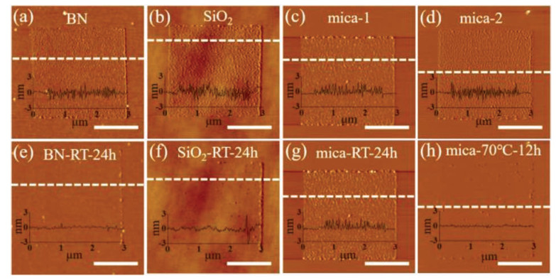
In addition, we research the self-healing process of monolayer HSP film on h-BN, SiO2/Si and mica substrates (Fig. 3). The monolayer HSP films on different substrates are destroyed in similar degree which the amplitude of the scratch is about 2 nm (Figs. 3a–d). It can be seen that HSP molecules pile up on the sample surface at the scratching end. This pile-up phenomenon is almost always observed after scratching sample surface, and is evidence that the tip drags HSP molecules during the process. The film on h-BN substrate becomes smooth without pinholes after 24 h at RT, showing the fastest healing response compared with the films on other substrates. There are some residual pinholes of HSP film on SiO2/Si substrate and the right edge of destroyed area is not healed because of serious damage (Fig. 3f). There is almost no healing phenomenon after 24 h at RT for film on mica substrate (Fig. 3g). However, healing response on the mica substrate can be promoted by heating film at 70 ℃ for 12 h (Fig. 3h).

|
Download:
|
| Fig. 3. (a-d) AFM image of destroyed monolayer HSP film on h-BN, SiO2/Si, mica-1 and mica-2 substrate, respectively. (e-h) AFM images of destroyed monolayer HSP film after 24 h at RT on h-BN, SiO2/Si, mica-1 substrate and after 12 h at 70 ℃ on mica-2 substrate, respectively. The scale bars are 1 μm. | |
The self-healing is a molecular re-alignment and reassembly process. Labile bonds play a critical role in this process that allows rapid structural rearrangements along with breaking and rebuilding of the bonds [23]. The hydrogen bond is the driving force for self-healing of the monolayer HSP film similar with the 3D self-healing process. However, substrates have remarkable influence in the case of the self-healing process at the 2D limit (Fig. S8 in Supporting information). Owing to the absorption of water molecules in the atmosphere, there is a water nanofilm on the surface of the h-BN or SiO2/Si substrate [24]. The molecule-substrate interactions on these substrates are hydrogen bond and Van Der Waals force, and the self-healing on h-BN substrate is better as the result of the smooth surface of the h-BN [25]. Mica is consisted of KAl2(Si3Al)O10(OH)2 which has negatively charged octahedral aluminosilicate layers [26]. Amine headgroup of HSP molecules adsorbs on water nanofilm of mica substrate and -NH2 protonation provides the electrostatic anchoring with the negatively charged surface of mica. According to the literatures, the energy of the electrostatic interaction is a few tens of kJ/mol [27]. In addition, hydrogen bond and van der Waals force also exist in the case of mica-HSP. Therefore, the interaction of mica-HSP should be stronger than that of HSP with h-BN or SiO2/Si substrate. This result can be proved by comparing the destruction of the first and the second HSP layers (Fig. S9 in Supporting information). On mica substrate, second layer can be more easily destroyed than the first layer under the same tip force. It means that the interaction of molecule-substrate is stronger than molecule-molecule interaction. On h-BN or SiO2/Si substrate, the results are opposite. It verifies the fact that the interaction of mica-HSP is stronger than the interaction of HSP with h-BN or SiO2/Si substrate.
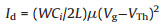
In the application, SiO2 dielectric modified with HSP selfassembled monolayer (SAM) is used in CuPc FETs. The device has a bottom-gated top-contact configuration as shown in Fig. 4a. Transfer and output characteristics of the CuPc FETs on HSP/SiO2/Si and on SiO2/Si are illustrated in Figs. 4b–e. The transfer characteristics of CuPc FETs are measured by scanning gate voltage (Vg) from +60 V to -60 V at a constant drain voltage (Vd) of -60 V corresponding to the saturation region. The hole field-effect mobility (μ) in saturation region is extracted from a plot of drain current1/2 (Id1/2) versus Vg using the following equation:

|
Download:
|
| Fig. 4. (a) Schematic diagram of a bottom-gate top-contact CuPc FETs. (b, c) Transfer characteristics of CuPc FETs (b) on HSP/SiO2/Si and (c) on SiO2/Si. (d, e) Output characteristics of CuPc FET (d) on HSP/SiO2/Si and (e) on SiO2/Si. (f) Schematic diagram of the CuPc FETs fabricated on bare SiO2/Si or on SiO2/Si with HSP monolayer. | |
|
where L and W are the length and width of the channel, Ci is the capacitance per unit area of the dielectric and VTh is the threshold voltage. The obtained mobility value of CuPc on HSP/SiO2/Si is 1.04 × 10⁻³ cm2 V-1 s-1, higher than the value on SiO2/Si (6.9 × 10⁻⁴ cm2 V-1 s-1). AFM images show that the grain size of CuPc on HSP/SiO2/Si is larger than that on SiO2/Si (Fig. S10 in Supporting information), thus avoiding the grain boundaries which lead to the scattering of the charge carriers. As shown in Fig. S11 (Supporting information), the HSP layer with self-healing property keeps the surface of SiO2/Si smooth, which reduces the charge carrier scattering at the semiconductor/dielectric interface [28].
In summary, we grow large-area self-healing monolayer HSP film and demonstrate the self-healing process which can be modulated by the substrate and temperature. The self-healing process at the 2D limit prefers the high temperature and the smooth substrate with weak molecule-substrate interaction. Furthermore, this self-healing monolayer HSP film can improve mobility of CuPc FETs, as larger grain size CuPc is grown on HSP/ SiO2/Si and the smooth surface of HSP film reduces the charge carrier scattering at the semiconductor/dielectric interface. This work extends our understanding of the self-healing process of polymer to the 2D space for the first time, to the best of our knowledge, which should be valuable for both the fundamental research and the potential applications of the 2D functional selfhealing material in the future.
AcknowledgmentsThis work was supported by National Program for Thousand Young Talents of China, the National Natural Science Foundation of China (Nos. 51773041, 21544001, 21603038), Shanghai Committee of Science and Technology in China (No. 18ZR1404900), and Fudan University.
Appendix A. Supplementary dataSupplementary material related to this article can be found, in the online version, at doi:https://doi.org/10.1016/j.cclet.2019.01.008.
| [1] |
J.F. Patrick, M.J. Robb, N.R. Sottos, J.S. Moore, S.R. White, Nature 540 (2016) 363-370. DOI:10.1038/nature21002 |
| [2] |
R.J. Wojtecki, M.A. Meador, S.J. Rowan, Nat. Mater. 10 (2011) 14-27. DOI:10.1038/nmat2891 |
| [3] |
S.R. White, P.H. Geubelle, Nat. Nanotechnol. 5 (2010) 247-248. DOI:10.1038/nnano.2010.66 |
| [4] |
M.D. Hager, P. Greil, C. Leyens, S. van der Zwaag, U.S. Schubert, Adv. Mater. 22 (2010) 5424-5430. DOI:10.1002/adma.201003036 |
| [5] |
M. Nakahata, Y. Takashima, H. Yamaguchi, A. Harada, Nat. Commun. 2 (2011) 511. DOI:10.1038/ncomms1521 |
| [6] |
Y. Chen, A.M. Kushner, G.A. Williams, Z. Guan, Nat. Chem. 4 (2012) 467-472. DOI:10.1038/nchem.1314 |
| [7] |
S. Banerjee, R. Tripathy, D. Cozzens, ACS Appl. Mater. Interfaces 7 (2015) 2064-2072. DOI:10.1021/am508096c |
| [8] |
K. Kratz, A. Narasimhan, Nat. Nanotechnol. 7 (2012) 87-90. DOI:10.1038/nnano.2011.235 |
| [9] |
B.J. Blaiszik, S.L. Kramer, M.E. Grady, D.A. McIlroy, S.R. White, Adv. Mater. 24 (2012) 398-401. DOI:10.1002/adma.201102888 |
| [10] |
S.A. Odom, S. Chayanupatkul, S.R. White, J.S. Moore, Adv. Mater. 24 (2012) 2578-2581. DOI:10.1002/adma.v24.19 |
| [11] |
P. Cordier, F. Tournilhac, C. Soulie-Ziakovic, L. Leibler, Nature 451 (2008) 977. DOI:10.1038/nature06669 |
| [12] |
B.C. Tee, C. Wang, R. Allen, Z. Bao, Nat. Nanotechnol. 7 (2012) 825-832. DOI:10.1038/nnano.2012.192 |
| [13] |
H. Wang, B. Zhu, W. Jiang, et al., Adv. Mater. 26 (2014) 3638-3643. DOI:10.1002/adma.v26.22 |
| [14] |
Y. Sun, J. Sun, W. Liu, et al., Adv. Mater. 28 (2016) 2455-2461. DOI:10.1002/adma.201504723 |
| [15] |
C. Wang, H. Wu, Z. Chen, et al., Nat. Chem. 5 (2013) 1042-1048. DOI:10.1038/nchem.1802 |
| [16] |
H. Yang, D. Qi, Z. Liu, et al., Adv. Mater. 28 (2016) 9175-9181. DOI:10.1002/adma.201602994 |
| [17] |
X. Zhuang, Y. Mai, D. Wu, F. Zhang, X. Feng, Adv. Mater. 27 (2015) 403. DOI:10.1002/adma.v27.3 |
| [18] |
G. Liu, J. Liu, X. Ye, et al., Angew. Chem. 56 (2017) 198-202. DOI:10.1002/anie.201609667 |
| [19] |
E.S.H. Kang, H. Zhang, W. Donner, H.V. Seggern, Adv. Mater. 29 (2017) 1604833. DOI:10.1002/adma.201604833 |
| [20] |
H. Sun, X. You, Y.S. Jiang, et al., Angew. Chem. Int. Ed. 53 (2014) 9526-9543. DOI:10.1002/anie.201405145 |
| [21] |
C. Stefaniu, A. Carmine, Q. Verolet, et al., Langmuir 31 (2015) 1296-1302. DOI:10.1021/la5039987 |
| [22] |
D. Qiang, G. Chen, T. Andritsch, Insulation and Dielectric Phenomena (CEIDP) Electrical, IEEE 439 (2015) 439-442. |
| [23] |
F. Solomon, V. Kolmakov, V. Yashin, et al., J. Chem. Phys. 134 (2011) 084901. DOI:10.1063/1.3556744 |
| [24] |
X. Lin, Y. Xu, A.A. Hakro, et al., J. Mater. Chem. C 1 (2013) 1618-1621. DOI:10.1039/c2tc00570k |
| [25] |
C. Whitehouse, J. Fang, A. Aggeli, et al., Angew. Chem. 44 (2005) 1965-1972. DOI:10.1002/(ISSN)1521-3773 |
| [26] |
H. Li, F. Zhang, Y. Zhang, et al., J. Phys. Chem. B 113 (2009) 8795. |
| [27] |
J.J. Benítez, J.A. Heredia-Guerrero, M.A. San-Miguel, H.C. Galloway, J. Phys. Chem. B 122 (2018) 493-499. DOI:10.1021/acs.jpcb.7b03603 |
| [28] |
X.N. Sun, C.A. Di, Y.Q. Liu, J. Mater. Chem. 20 (2010) 2599-2605. DOI:10.1039/b921449f |