 2019, Vol. 30


b Innovation Center for Textile Science and Technology, Donghua University, Shanghai 200051, China;
c Academy of Fundamental and Interdisciplinary Sciences, Harbin Institute of Technology, Harbin 150080, China
Lithium-ion batteries (LIBs) with higher power and energy density as well as better rate capability are of utmost importance for ever-growing demands in grid storage and electric/hybrid electric vehicles. In this sense, the graphitic anode based on an intercalation mechanism fails to satisfy these standards, mainly due to its low theoretical capacity (372 mAh/g), and considerable risk of lithium plating when subjected to fast charging. Instead, as an alloying type anode material, silicon has the highest theoretical capacity of 4200 mAh/g when 4.4 mol of Li+ ions are accommodated by per mole of Si (Li22Si5) [1-4]. Additionally, silicon is the second most abundant element in the earth's crust, and thus has the potential to be provided in a large quantity.
It is worth noting, however, that the following issues should be addressed before silicon can be engineered into an industrially viable anode: First of all, the huge volume expansion of silicon (300%–400%) during repeated lithiation–delithiation causes the structural instability, and the parasitic formation of a solid– electrolyte interface (SEI) film on the freshly exposed silicon surfaces. On the one hand, the structural instability will lead to the pulverization of the silicon anode, and the loss of electrical contact. On the other hand, the excessive growth of the SEI film will result in the continuous consumption of the electrolyte and "live" Li+ ions during cycling. Things are made worse by the inevitable side reactions with the electrolyte, and the low intrinsic conductivity (~10–3 S/cm) of silicon. All these deficiencies are eventually responsible for the poor cyclability and unsatisfactory rate capability suffered by the silicon anode [5-10].
To buffer the volume expansion of silicon which was identified as one of the major reasons for the capacity fading especially at high rates, two different strategies were proposed: One was to design a hollow structure [11-15], whose free volume was expected to accommodate the stress stemming from continuous expansion–contraction [16, 17]. The other relied on the formation of an oxide or carbon shell, in which the active material, i.e., silicon yolk, was encapsulated. The void space created in between could force the silicon yolk to expand inward upon lithiation without breaking the oxide or carbon shell. Therefore, the resulting yolk–shell structure could survive from the mechanical stress fluctuations generated during repeated lithiation–delithiation, and keep the electrolyte away from the active material [18-28].
Despite the aforementioned achievements in optimizing the electrochemical performance, an insurmountable difficulty existed which inevitably set obstacles for their practical applications: In general, all precursors employed in the state-of-the-art researches, such as tetraethyl orthosilicate (TEOS) and SiCl4, exclusively originated from high-purity quartz by carbothermal reduction (≥2000 ℃), which was costly and energy consuming [29]. As such, several pioneering works adopted inexpensive natural resources (e.g., reeds and rice husks) as the precursors, in which silicon in the form of silicic acid (Si(OH)4 or Si(OH)3O–) was absorbed from the soil [30-33]. However, the silicon content in these natural resources was very low, being 15 wt%–20 wt% only. Instead, the reserves of sand in nature were immeasurable, which was therefore a sustainable and high-efficiency silicon source which held great promise in industry. In preliminary attempts, sand was converted to silicon by magnesiothermic reduction [29, 34]. Whereas, this method was largely restricted by high reaction temperature (≥650 ℃), numerous side reactions as well as low yield of silicon [35]. In this context, low-temperature aluminothermic reduction was recently adopted by ourselves and others as an alternative method to synthesize crystalline silicon from silica [36, 37].
Here we report, for the first time, aluminothermic reduction enabled synthesis of hollow silicon microspheres from sand, which energetically combines a cost-effective silicon source with an energy-efficient, high-yield methodology — the two key factors demanded for industrialization. These hollow silicon microspheres are further encaged in a carbon shell, resulting in hollow Si@void@C yolk–shell microspheres. This unique, hierarchical arrangement smartly integrates the merits of hollow structure and yolk–shell structure, and can therefore effectively accommodate the diffusion-induced stress by providing the hollow interior and the void space. Moreover, the carbon shell can not only function as an electrolyte-blocking layer to protect the silicon yolk from undesirable side reactions and SEI formation, but also act as a conductive framework to reduce the resistance to electron and Li+ ion transport. Benefiting from these synergistic effects, the hollow Si@void@C yolk–shell microspheres exhibit superior long-term cyclability and rate capability, which lay a basis for the development of a high-performance silicon-based anode of advanced LIBs.
The raw material, i.e., natural sand, was collected from Hobq Desert, the seventh largest desert in China. The sand was smashed in a planetary ball-mill at 400 rpm for 2 h, and soaked in HCl/HNO3 at 60 ℃ for 4 h to remove the impurities. A white-colored intermediate, i.e., purified silica, was obtained by washing with deionized water, and drying. Hollow silicon microspheres were synthesized by low-temperature aluminothermic reduction as reported by us previously [36]. In a typical experiment, 1 g of silica and 1–1.5 g of aluminum powder (1–3 μm) were ground with 12 g of AlCl3 for 10 min. The mixture was then loaded in a stainless steel autoclave. After three times of degassing, the autoclave was filled with nitrogen, and heated at 270 ℃ for 10 h in an electric oven. The obtained powder was dissolved in HCl/ethanol solution three times, washed with HF, filtered, and vacuum-dried at 60 ℃ for 10 h to obtain hollow silicon microspheres.
Typically, 0.5 g of hollow silicon microspheres were dispersed in a mixed solution containing 280 mL of ethanol, 70mL of deionized water, and 5 ml of ammonia (28%) under sonication for 30 min. Then, 1.0 mL of TEOS (98%) dispersed in 5 mL of ethanol was added dropwise every 1 h (4 mL of TEOS and 20 mL of ethanol in total), and the reaction continued for 10 h at ambient temperature under stirring. After being centrifuged and washed with deionized water and ethanol three times, hollow Si@SiO2 core–shell microspheres were obtained [21]. Then, 1 g of hollow Si@SiO2 core–shell microspheres were dispersed in a mixture of 600 mL of deionized water and 200 mL of ethanol under sonication, followed by the addition of 1.5 g of CTAB. The mixed solution was stirred for 30 min, to which 0.32 g of resorcinol and 0.5 mL of formaldehyde were added. After the addition of 2 mL of ammonia, the final mixture was stirred at ambient temperature for 24 h, and hollow Si@SiO2@RF core–shell microspheres were obtained after centrifugation and drying [38, 39]. The hollow Si@SiO2@RF core–shell microspheres were then calcined in argon atmosphere at 800 ℃ for 2 h at a heating rate of 5 ℃/min. After being washed with HF, hollow Si@void@C yolk–shell microspheres were obtained. For comparison, hollow carbon microspheres were obtained by etching the silicon yolk with NaOH solution. The commercialized silicon microparticles (1–5 μm) were purchased from Alfa Aesar.
The working electrode was prepared by coating a slurry of 70 wt% active material, 20 wt% carbon fiber, and 10 wt% binder (sodium alginate and carboxymethyl cellulose at 1:1 w/w) in deionized water onto a copper foil. After being dried at 60 ℃ for 10 h, the electrode was cut into discs with a diameter of 14 mm, and the mass loading of the active material was 1.0–1.1 mg/cm2. Li foil was used as the counter electrode. The test cell was assembled in an argon-filled glove box. The electrolyte was 1 mol/L LiPF6 in a mixture of dimethyl carbonate and ethylene carbonate (molar ratio = 1:1) with 10 vol% fluorethylene carbonate. The galvanostatic tests were carried out at ambient temperature by using a LANDCT2001 A cycler. The CV tests were carried out by using an electrochemical workstation (Chi660e) between 0.01 V and 1.5 V vs. Li/Li+ at a scan rate of 0.1 mV/s. The EIS tests were carried out within a frequency range from 100 kHz to 0.01 Hz. The capacity was calculated based on the whole hollow Si@void@C yolk–shell microspheres.
Transmission electron microscopy (TEM) was performed by a Hitachi HT7700 microscope operated at an accelerating voltage of 100 kV. High-resolution TEM (HRTEM) and scanning transmission electron microscopy (STEM) were performed by a JEOL JEM-2100F microscope operated at an accelerating voltage of 120 kV. Scanning electron microscopy (SEM) was performed by a Tescan Vega3 microscope operated at an accelerating voltage of 20 kV. X-ray diffraction (XRD) was performed by a Bruker D8 Advanced X-ray diffractometer with Cu Kα radiation (λ = 0.154 nm). X-ray fluorescence spectroscopy (XRF) was performed by a Shimadzu EDX- 7000. X-ray photoelectron spectroscopy (XPS) was performed by a Thermo Scientific Escalab 250Xi spectrometer. Raman was performed by a RamanMicro 300 spectrometer (PerkinElmer, USA) with a 514 nm incident laser. Thermogravimetric analysis (TGA) was performed by a Shimadzu DTG-60 from room temperature to 800 ℃ in air at a heating rate of 10 ℃/min. The nitrogen adsorption–desorption isotherms at 77 K were measured on a Quadrasorb Si-Kr/MP (Quantachrome, USA). The specific surface area was calculated by using the Brunauer-Emmett-Teller (BET) method. The pore sizes and pore volumes were estimated by using the Barrett–Joyner–Halenda (BJH) method.
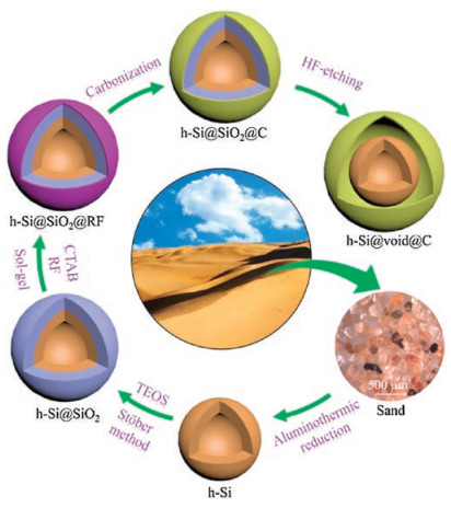
The entire process for the synthesis of hollow Si@void@C yolk– shell microspheres is schematically depicted, step by step, in Scheme 1. Starting from natural sand collected from Hobq Desert, low-temperature aluminothermic reduction was employed to synthesize hollow silicon microspheres by an Ostwald ripening process as will be discussed in detail below. The hollow silicon microspheres were coated with a TEOS-derived silica layer by a well-established Stöber method [21], resulting in hollow Si@SiO2 core–shell microspheres terminated with plenty of -OH groups. These negatively charged surface functional groups were ready to adsorb positively charged cetyltrimethyl ammonium bromide (CTAB) molecules, which were then encapsulated by resorcinol and formaldehyde through electrostatic attraction. After copolymerization by a sol-gel method, hollow Si@SiO2@RF core–shell microspheres were obtained, which were further converted to hollow Si@SiO2@C core–shell microspheres through carbonization of the RF resin [38, 39]. Finally, the SiO2 layer was etched away by HF, leaving hollow Si@void@C yolk–shell microspheres.

|
Download:
|
| Scheme 1. Process for the synthesis of hollow Si@void@C yolk–shell microspheres: (ⅰ) synthesis of hollow silicon microspheres from sand by aluminothermic reduction, (ⅱ) coating with a TEOS-derived silica layer by a Stöber method, (ⅲ) formation of a RF layer by CTAB-assisted electrostatic attraction and copolymerization of resorcinol and formaldehyde, (ⅳ) carbonization of the RF layer, and (ⅴ) etching of the silica layer by HF to obtain hollow Si@void@C yolk–shell microspheres. | |
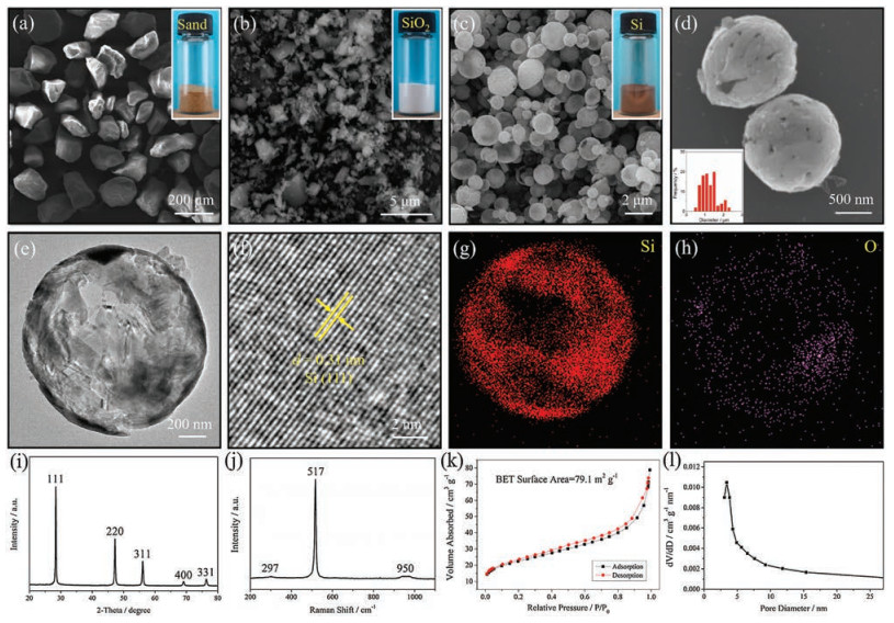
SEM was used to confirm the successful synthesis of the hollow silicon microspheres from sand by aluminothermic reduction. Fig. 1a shows an SEM image of coarse sand grains of several hundred micrometers, which have a typical yellow-brown color. These sand grains were firstly smashed in a planetary ball-mill to reduce the sizes, and then soaked in HCl/HNO3 to remove the impurities. A white-colored intermediate, i.e., purified silica, was obtained, as shown in Fig. 1b. It can be unambiguously seen that the sizes of these silica particles are largely reduced, ranging from several micrometers to several hundred nanometers. After being mixed with aluminum in molten AlCl3, silica could be converted to silicon through a unique redox reaction:

|
(1) |

|
Download:
|
| Fig. 1. SEM images of (a) sand, (b) acid-washed sand (purified silica), and (c, d) hollow silicon microspheres, (e) TEM and (f) HRTEM images of hollow silicon microspheres and the corresponding (g) Si and (h) O maps, (i) XRD pattern, (j) Raman spectrum, (k) nitrogen adsorption–desorption isotherms, and (l) pore-size distribution of hollow silicon microspheres. The insets in (a)–(c) show the photographs of sand, purified silica, and hollow silicon microspheres. The inset in (d) shows the diameter distribution of hollow silicon microspheres. | |
An Ostwald ripening process was responsible for the formation of the hollow silicon microspheres: On the time course, three different stages could be witnessed: At first, the surfaces of the silica particles, upon exposure to aluminum, were subjected to aluminothermic reduction, where small silicon crystallites were formed. These newly formed, small silicon crystallites gradually grew into large, platelet-like crystals in order to reduce the surface area, which was favorable for minimizing the surface energy (Fig. S1a in Supporting information). With increasing reaction time, these platelet-like crystals had a strong tendency to coalesce, and merge into a spherical structure since its surface area was the minimum, as shown in Figs. S1b and c (Supporting information). At the final stage, the residual silica continued to be reduced, while the inner silicon crystallites were dissolved and re-deposited on the out surfaces as driven by their higher surface energy. In result, hollow silicon microspheres were eventually obtained (Fig. S1d in Supporting information).
Typical SEM images of the hollow silicon microspheres at different magnifications are shown in Figs. 1c and d. As seen from these images, aluminothermic reduction has a fairly high yield of hollow silicon microspheres, and the product has a perfect spherical structure with sizes mainly centered at 0.2–2 μm (inset). A TEM image of a hollow silicon microsphere, as shown in Fig. 1e, clearly displays the sharp contrast between the "lighter" cavity and the "darker" wall. Statistics on the wall thickness of the hollow silicon microspheres, based on TEM observation, show a value centered at 50 ± 25 nm (Fig. S2 in Supporting information). Under HRTEM observation (Fig. 1f), a lattice fringe spacing of 0.31 nm is in good agreement with the (111) plane of crystalline silicon [40, 41]. The corresponding energy-dispersive X-ray spectroscopy (EDS) maps of Si and O are shown in Fig. 1g and h. A dense and uniform distribution of elemental Si can be seen corresponding to the wall of the hollow silicon microsphere. The distribution of elemental O is sparse, which arises from the inevitable surface oxidation during exposure to air [42].
The silicon content was determined by XRF, as shown in Table S1 in Supporting information, which increases significantly from 73.22 wt% for sand to 99.41 wt% for hollow silicon microspheres. This purity is even higher than that of commercialized silicon (Alfa Aesar), demonstrating a very high efficiency of our aluminothermic reduction method. The XRD pattern of the hollow silicon microspheres is given in Fig. 1i, which discloses prominent peaks attributed to the (111), (220), (311), (400), and (331) planes of crystalline silicon (JCPDS card No. 77–2111). In contrast, the XRD patterns of sand and washed sand (purified silica) shows peaks indexed to quartz silica (JCPDS card No. 46– 1405), another proof of the successful reduction of silica to silicon (Fig. S3 in Supporting information). Fig. 1j provides the Raman spectrum of the silicon hollow microspheres, which is in consistent with the previous report on crystalline silicon [43]. The prominent peak at 517 cm–1 is assigned to the scattering of the first-order optical phonon of silicon, and the two broad peaks at 297 and 950 cm–1 are assigned to the scattering of two transverse acoustic phonons and two transverse optical phonons, respectively. The nitrogen adsorption–desorption isotherms of the hollow silicon microspheres obey a typical type Ⅳ hysteresis loop (Fig. 1k). The surface area, as measured by the BET method, is 79.1 m2/g. The pore size distribution has a peak centered at 3.4 nm as estimated by the BJH method, characteristic of a mesoporous structure (Fig. 1l).
After a carbon shell was formed on the hollow silicon microspheres through carbonization of the RF resin, the color evolved from dark brown to black (Fig. S4 in Supporting information). The morphological change from the hollow silicon microspheres to the hollow Si@void@C yolk–shell microspheres is presented in Figs. 2a and b. Obviously, after carbonization of the RF resin, the hollow silicon microspheres are encaged in a homogeneous carbon shell, while they stay semi-detached from each other, thus creating well-defined void space in between. Interestingly, even when the silicon yolk was etched away by NaOH, the carbon shell can still preserve its original morphology without being broken or collapsed (Fig. S6 in Supporting information). Besides, the carbon shell is crumpled, characteristic of its high flexibility and elasticity. The thickness of the carbon shell is very thin, showing a value centered at 20 ± 10 nm (Fig. S7 in Supporting information), which is advantages for ensuing a high fraction of the active material (silicon yolk).

|
Download:
|
| Fig. 2. TEM images of (a) hollow Si microspheres and (b) hollow Si@void@C yolk–shell microspheres, (c) STEM image of hollow Si@void@C yolk–shell microspheres and (d) the corresponding C, Si, and O maps. | |
Further evidence of the hollow Si@void@C yolk–shell microspheres was identified by a dark-field STEM image and the corresponding EDS mapping, as shown in Figs. 2c and d. The elemental information of Si and C can be clearly distinguished corresponding to the yolk and the shell, respectively. Additionally, the empty space in the silicon yolk, as well as between the silicon yolk and the carbon shell, can also be seen. The negligible elemental information of O is in consistent with Fig. 1h, indicating that the silicon yolk was not further oxidized during the synthesis of the carbon shell. Note that the hollow interior and the void space, hand in hand, allow enough room for the volume expansion without causing deformation or rupture. Besides, the thin and homogeneous carbon shell can prevent the silicon yolk from direct contact with the electrolyte, so the SEI film can only be stably formed on the outer surfaces of the hollow Si@void@C yolk–shell microspheres. The carbon shell can further reduce the resistance to electron and Li+ ion transport. All these merits are expected to contribute to improved long-term cyclability and rate capability as will be proven below.
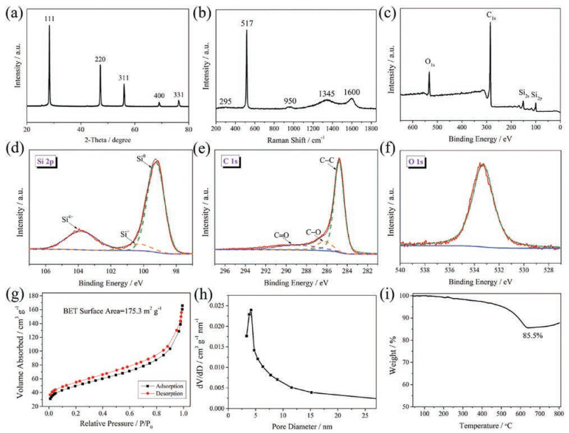
Fig. 3a shows the XRD pattern of the hollow Si@void@C yolk–shell microspheres, which is identical to that of the hollow silicon microspheres (Fig. 1i), suggesting that the crystalline nature of the silicon yolk was well protected during the synthesis of the carbon shell. Although the carbon shell itself has a broad peak centered at ~25° (Fig. S8 in Supporting information), its crystallinity is rather weak compared to the silicon yolk, so this peak is invisible in Fig. 3a. The Raman spectrum of the hollow Si@void@C yolk–shell microspheres is given in Fig. 3b. In addition to the above-analyzed characteristic peaks of the silicon yolk, two more peaks occur which can be assigned to the carbon shell. The peak located at 1345 cm–1, also known as the D peak, originates from the in-plane breathing mode of the A1g symmetry due to the presence of sixfold aromatic rings. The other peak residing at 1600 cm–1, also known as the G peak, is related to the E2g mode, and arises from the vibration of the sp2-hybridized carbon atoms in the graphitic sheets [44].

|
Download:
|
| Fig. 3. (a) XRD pattern, (b) Raman spectrum, (c) wide-scan survey, high-resolution (d) Si 2p, (e) C 1s, and (f) O 1s XPS spectra, (g) nitrogen adsorption–desorption isotherms, (h) pore-size distribution, and (i) TGA curve of hollow Si@void@C yolk–shell microspheres. | |
XPS was conducted to investigate the metal oxidation state and chemical composition of the hollow Si@void@C yolk–shell microspheres. Fig. 3c shows the wide-scan survey, in which the signals associated with Si, C, and O can be clearly seen. In the highresolution Si 2p spectrum (Fig. 3d), the peaks located at 99.3 and 103.5 eV are assigned to Si° and Si4+, respectively [45]. It is apparent that the peak intensity of Si4+ is significantly weaker than that of Si°, indicating the successful formation of silicon. The peak between 99.3 eV and 103.5 eV can be ascribed to SiOx (0 < x < 2), whose existence is the result of slight oxidation of silicon during exposure to air [46]. The high-resolution C 1s spectrum, as shown in Fig. 3e, can be deconvoluted into three peaks, and the major peak centered at 284.8 eV is attributed to the free carbon (C-C). The other two peaks at 286.2 and 288.8 eV are assigned to C-O and C=O bands, respectively, indicating the presence of a small amount of RF resin which was not converted to carbon completely [47, 48]. Fig. 3f displays the high-resolution O 1s spectrum, in which the single peak situated at 533.4 eV comes from the absorbed oxygen, tape substrate, C-O, C=O and/or Si-O bonds [49].
The nitrogen adsorption–desorption isotherms of the hollow Si@void@C yolk–shell microspheres also obey the type Ⅳ hysteresis loop (Fig. 3g). The BET surface area increases significantly to 175.3 m2/g, which is due to the creation of more surfaces resulting from the presence of the carbon shell. The mesoporous structure is still preserved with a pore distribution centered at 4.2 nm (Fig. 3h). The large surface area combined with high porosity ensures a good effect on buffering the volume expansion and, thus, minimizing the capacity fading due to the SEI film degradation and the active material pulverization [50-52]. To quantitatively determine the contents of the silicon yolk and the carbon shell, TGA was conducted, whose result is presented in Fig. 3i. The obvious weight loss in the range of 300–600 ℃ corresponds to the combustion of carbon. The gradual increase of the weight from 600 ℃ is attributed to the oxidation of silicon in air since it is stable at below this temperature [27, 53, 54]. As such, the content of the silicon yolk accounts for 85.5 wt% of the hollow Si@void@C yolk–shell microspheres.
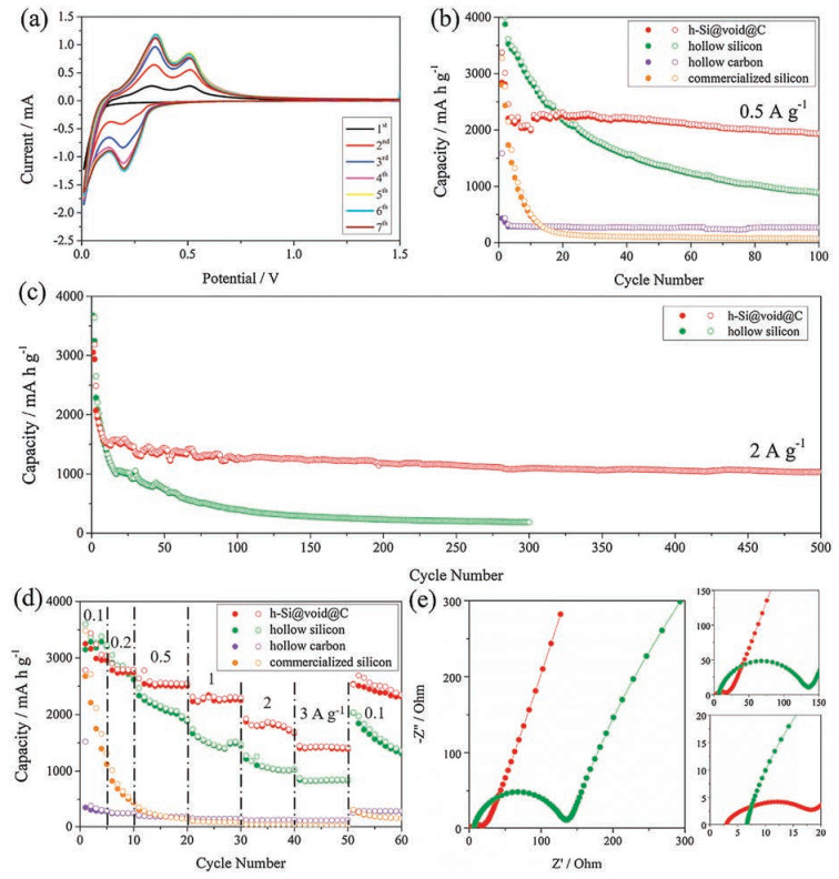
The lithium storage characteristics of the hollow Si@void@C yolk–shell microspheres were investigated by the cyclic voltammetry (CV) tests. Fig. 4a shows the first seven CV curves of the hollow Si@void@C yolk–shell microspheres at a scan rate of 0.1 mV/s from 0.01 V to 1.5 V vs. Li/Li+. In the first cathodic scan, the weak peak located at around 0.7 V can be attributed to the formation of the SEI film [25, 55]. In the following scan, the reduction peak at around 0.2 V, corresponding to the Li-insertion process of crystalline silicon to form amorphous LixSi [23]. In the anodic scan, two oxidation peaks at around 0.35 V and 0.51 V, which can be ascribed to the transition from LixSi to amorphous silicon [27]. Moreover, the current increases with the first five cycles, suggesting an activation process of the hollow Si@void@C yolk–shell microspheres [56-58]. In the 6th and 7th cycles, the CV curves of the hollow Si@void@C yolk–shell microspheres are almost superposed, suggesting very good cyclability.

|
Download:
|
| Fig. 4. (a) First seven CV curves of hollow Si@void@C yolk–shell microspheres, (b) cycle behaviors of hollow silicon microspheres, hollow Si@void@C yolk–shell microspheres, hollow carbon microspheres and commercialized silicon at a current density of 0.5 A/g, (c) cycle behaviors of hollow Si microspheres and hollow Si@void@C yolk–shell microspheres at a current density of 2 A/g, (d) rate capabilities of hollow Si microspheres, hollow Si@void@C yolk–shell microspheres, hollow carbon microspheres and commercialized silicon at different current densities, and (e) Nyquist plots of hollow Si microspheres and hollow Si@void@C yolk–shell microspheres. | |
The cycle behavior of the hollow Si@void@C yolk–shell microspheres at a current density of 0.5 A/g is presented in Fig. 4b. For comparison, the cycle behaviors of the hollow silicon microspheres, hollow carbon microspheres and commercialized silicon are also presented. As seen from this figure, the commercialized silicon delivers an initial capacity of >3000 mAh/g, which drastically drops to only 160 mAh/g after 20 cycles. This rapid capacity fading results from the huge volume expansion, the excessive SEI growth and the hampered electron and Li+ ion transport, which makes commercialized silicon itself impossible as a practical anode. The hollow carbon microspheres exhibit good cycle stability due to high mechanical flexibility and conductivity, while the absolute value of the reversible capacity is very low which is characteristic of a carbon anode. As for the hollow silicon microspheres, a reversible capacity of 889 mAh/g is delivered after 100 cycles, accounting for ~22% of the initial value merely. Although the cycle stability is improved to some extent compared to the commercialized silicon, mainly due to the unique hollow structure which can buffer the volume expansion, it is still far from being satisfactory. Note that this value is different from our previous report [36], which is due to different active material loadings, as well as different electrolyte, binder and conductive additive used in the two works. When a carbon shell is formed on the hollow silicon microspheres, the resulting hollow Si@void@C yolk–shell microspheres exhibit an excellent cycle behavior, delivering a strikingly high reversible capacity of 1942 mAh/g after 100 cycles.
The long-term cyclability of the hollow Si@void@C yolk–shell microspheres, especially at a high rate of 2 A/g, is shown in Fig. 4c. Interestingly, superior long-term cyclability is witnessed, translating into a reversible capacity as high as 1040 mAh/g after 500 cycles. In contrast, the hollow silicon microspheres alone deliver a reversible capacity of only 185 mAh/g after 300 cycles, once again verifying the significance of introducing the carbon shell: It can not only function as an electrolyte-blocking layer to protect the silicon yolk from undesirable side reactions and SEI formation, but also act as a conductive framework to reduce the resistance to electron and Li+ ion transport. Moreover, the combined action of the hollow structure and the yolk–shell structure can effectively accommodate the diffusion-induced stress by providing the hollow interior and the void space. Note that the reversible capacity was calculated based on the total mass of the hollow Si@void@C yolk–shell microspheres, including the fractions from the carbon shell and the silicon yolk. The mass loading of the active material was 1.0– 1.1 mg/cm2, which made a comparison with other silicon-based anodes fair and possible. The long-term cyclability and reversible capacity of our hollow Si@void@C yolk–shell microspheres are among the best when compared to the previously reported, various Si/C composites, as summarized in Table S2 in Supporting information. Particularly when we consider the fact that the hollow Si@void@C yolk–shell microspheres are derived from a cost-effective silicon source (natural sand) with an energyefficient, high-yield methodology (low-temperature aluminothermic reduction), which lays a basis for developing a fast and stable silicon anode for advanced LIBs.
The rate capabilities are also compared and shown in Fig. 4d. When cycled at current densities of 0.1, 0.2, 0.5, 1, 2, and 3 A/g, the hollow Si@void@C yolk–shell microspheres deliver reversible capacities up to 3041, 2792, 2551, 2294, 1686, and 1416 mAh/g, which are significantly higher than those of their components (hollow silicon and carbon microspheres) as well as the commercialized silicon. When the current density is recovered to 0.1 A/g, the reversible capacity returns to 2353mAh/g after 10 cycles. Note that the reversible capacity of the hollow Si@void@C yolk–shell microspheres decreases a little after deep cycling, which means a moderate degree of structural instability at high rates. However, this decrease is much lower than that of the hollow silicon microspheres, which justifies the effect of the carbon shell on stabilizing the whole electrode. The greater electrochemical performance of the hollow Si@void@C yolk–shell microspheres is elucidated by the electrochemical impedance spectroscopy (EIS) tests, as shown in Fig. 4e. The intercept of each plot with a horizontal axis at high frequency is Rs, which represents the equivalent series resistance (ESR) including all resistances coming from the electrolyte and the other parts of the cell. It can be seen that both plots have a single semicircle at high to medium frequency and an inclined line at low frequency, corresponding to the charge transfer resistance (Rct) through the electrode/electrolyte interface and solid-state diffusion of Li+ ions (W) in electrode material, respectively. The Rs value of the hollow Si@void@C yolk– shell microspheres is 3Ω, which is smaller than that (5 Ω) of the hollow silicon microspheres, rationalizing the role of the carbon shell as a conductive framework which facilitates the electron transport. Importantly, the much lower Rct value of the hollow Si@void@C yolk–shell microspheres compared to the hollow silicon microspheres (15 vs. 129Ω) verifies more active sites and better conductivity of the former. Moreover, the slope of the inclined line for the hollow Si@void@C yolk–shell microspheres is higher than that of the hollow silicon microspheres, which means a higher Li+ ion diffusivity of the former [59]. On the whole, the construction of the hollow Si@void@C yolk–shell microspheres not only enables easy electron transport and Li+ ion diffusion in the solid-state electrode material, but also reduces the charge transfer resistance through the electrode–electrolyte interface.
The superiority of the hollow Si@void@C yolk–shell microspheres over the hollow silicon microspheres, in terms of structural stability, is further analyzed by TEM observation after cycling combined with schematic description. As depicted in Fig. 5a, the hollow silicon microspheres will undergo expansion– contraction during repeated lithiation–delithiation, which will inevitably induce pulverization due to their structural rigidity. Therefore, the whole structure of the hollow silicon microspheres will be deformed seriously after cycling, as shown in Fig. 5b. This structural instability will further lead to the parasitic formation of a thick and non-uniform SEI film on the freshly exposed surfaces and, thus, the continuous consumption of the electrolyte and "live" Li+ ions during cycling. Moreover, the direct contact between the hollow silicon microspheres and the electrolyte will cause numerous undesirable side reactions. All these reasons result in the unsatisfactory cycle and rate performance of the hollow silicon microspheres. However, the hollow structure and the void space created in between have reserved the space for the expansion of silicon, and the carbon shell of the hollow Si@void@C yolk-shell microspheres remains intact (Fig. 5c). Therefore, the whole structure of the hollow Si@void@C yolk–shell microspheres will be well protected from cracking or deformation after cycling, as shown in Fig. 5d. In this sense, only a thin, compact and uniform SEI film is formed on the outer surface of the carbon shell. It is well known that the SEI film is almost impenetrable to the electrolyte molecules, so the electrolyte is unable to travel through the SEI film to the silicon yolk [53, 54]. As such, the superior structural stability of the hollow Si@void@C yolk–shell microspheres is responsible for preventing the excessive SEI growth and the undesirable side reactions, which eventually establishes a foundation for the greater electrochemical performance [60].

|
Download:
|
| Fig. 5. Schematic description of repeated lithiation/delithiation of (a) hollow silicon microspheres and (c) hollow Si@void@C yolk–shell microspheres, and the corresponding TEM images of (b) hollow silicon microspheres and (d) hollow Si@void@C yolk–shell microspheres after 100 cycles at 0.5 A/g. | |
In conclusion, we have reported aluminothermic reduction enabled synthesis of hollow silicon microspheres from sand, which energetically combines a cost-effective silicon source with an energy-efficient, high-yield methodology — the two key factors demanded for industrialization. These hollow silicon microspheres are further encaged in a carbon shell, resulting in hollow Si@void@C yolk–shell microspheres. This unique, hierarchical arrangement smartly integrates the merits of hollow structure and yolk–shell structure, and can therefore effectively accommodate the diffusion-induced stress by providing the hollow interior and the void space. Moreover, the carbon shell can not only function as an electrolyte-blocking layer to protect the silicon yolk from undesirable side reactions and SEI formation, but also act as a conductive framework to reduce the resistance to electron and Li+ ion transport. Benefiting from these synergistic effects, the hollow Si@void@C yolk–shell microspheres deliver a strikingly high reversible capacity of 1942 mAh/g at 0.5 A/g after 100 cycles, or 1040 mAh/g at 2 A/g after 500 cycles, which are among the best compared to the previously reported, various Si/C composites. We believe our research lays a basis for the development of a highperformance silicon-based anode for advanced LIBs.
AcknowledgmentWe thank the financial support from the National Natural Science Foundation of China (Nos. 51633003 and 21774069).
Appendix A. Supplementary dataSupplementary material related to this article can be found, in the online version, at doi:https://doi.org/10.1016/j.cclet.2018.08.018.
| [1] |
X. Zuo, J. Zhu, P. Müller-Buschbaum, Y.J. Cheng, Nano Energy 31 (2017) 113-143. DOI:10.1016/j.nanoen.2016.11.013 |
| [2] |
J.K. Lee, C. Oh, N. Kim, J.Y. Hwang, Y.K. Sun, J. Mater. Chem. A 4 (2016) 5366-5384. DOI:10.1039/C6TA00265J |
| [3] |
B. Liang, Y. Liu, Y. Xu, J. Power Sources 267 (2014) 469-490. DOI:10.1016/j.jpowsour.2014.05.096 |
| [4] |
M.L. Terranova, S. Orlanducci, E. Tamburri, et al., J. Power Sources 246 (2014) 167-177. DOI:10.1016/j.jpowsour.2013.07.065 |
| [5] |
J. Li, N.J. Dudney, X. Xiao, et al., Adv. Energy Mater. 5 (2015) 1401627. DOI:10.1002/aenm.201401627 |
| [6] |
J. Wang, X. Meng, X. Fan, et al., ACS Nano 9 (2015) 6576-6586. DOI:10.1021/acsnano.5b02565 |
| [7] |
T.T. Fister, J. Esbenshade, X. Chen, et al., Adv. Energy Mater. 4 (2014) 1301494. DOI:10.1002/aenm.201301494 |
| [8] |
R.B. Cervera, N. Suzuki, T. Ohnishi, et al., Energy Environ. Sci. 7 (2014) 662-666. DOI:10.1039/C3EE43306D |
| [9] |
B.M. Bang, J.I. Lee, H. Kim, J. Cho, S. Park, Adv. Energy Mater. 2 (2012) 878-883. DOI:10.1002/aenm.201100765 |
| [10] |
C. Yu, X. Li, T. Ma, et al., Adv. Energy Mater. 2 (2012) 68-73. DOI:10.1002/aenm.201100634 |
| [11] |
Y. Yao, M.T. McDowell, I. Ryu, et al., Nano Lett. 11 (2011) 2949-2954. DOI:10.1021/nl201470j |
| [12] |
M.P. Liu, C.H. Li, H.B. Du, X.Z. You, Chem. Commun. 48 (2012) 4950-4952. DOI:10.1039/c2cc17083c |
| [13] |
F.H. Du, B. Li, W. Fu, et al., Adv. Mater. 26 (2014) 6145-6150. DOI:10.1002/adma.201401937 |
| [14] |
J. Liang, X. Li, Q. Cheng, et al., Nanoscale 7 (2015) 3440-3444. DOI:10.1039/C4NR07642G |
| [15] |
Z.W. Zhou, Y.T. Liu, X.M. Xie, X.Y. Ye, ACS Appl. Mater. Interfaces 8 (2016) 7092-7100. DOI:10.1021/acsami.6b00107 |
| [16] |
Z. Wang, L. Zhou, X.W. Lou, Adv. Mater. 24 (2012) 1903-1911. DOI:10.1002/adma.v24.14 |
| [17] |
X.W. Lou, L.A. Archer, Z. Yang, Adv. Mater. 20 (2008) 3987-4019. DOI:10.1002/adma.v20:21 |
| [18] |
N. Liu, H. Wu, M.T. McDowell, et al., Nano Lett. 12 (2012) 3315-3321. DOI:10.1021/nl3014814 |
| [19] |
N. Liu, Z. Lu, J. Zhao, et al., Nat. Nanotechnol. 9 (2014) 187-192. DOI:10.1038/nnano.2014.6 |
| [20] |
X. Xiao, W. Zhou, Y. Kim, et al., Adv. Funct. Mater. 25 (2015) 1426-1433. DOI:10.1002/adfm.v25.9 |
| [21] |
J. Yang, Y.X. Wang, S.L. Chou, et al., Nano Energy 18 (2015) 133-142. DOI:10.1016/j.nanoen.2015.09.016 |
| [22] |
L. Zhang, R. Rajagopalan, H. Guo, et al., Adv. Funct. Mater. 26 (2016) 440-446. DOI:10.1002/adfm.v26.3 |
| [23] |
B. Li, R. Qi, J. Zai, et al., Small 12 (2016) 5281-5287. DOI:10.1002/smll.v12.38 |
| [24] |
Y. Jin, S. Li, A. Kushima, et al., Energy Environ. Sci. 10 (2017) 580-592. DOI:10.1039/C6EE02685K |
| [25] |
F.H. Du, Y. Ni, Y. Wang, et al., ACS Nano 11 (2017) 8628-8635. DOI:10.1021/acsnano.7b03830 |
| [26] |
H. Su, A.A. Barragan, L. Geng, et al., Angew. Chem. Int. Ed. 56 (2017) 10780-10785. DOI:10.1002/anie.201705200 |
| [27] |
S. Guo, X. Hu, Y. Hou, Z. Wen, ACS Appl. Mater. Interfaces 9 (2017) 42084-42092. DOI:10.1021/acsami.7b13035 |
| [28] |
X. Huang, X. Sui, H. Yang, et al., J. Mater. Chem. A 6 (2018) 2593-2599. DOI:10.1039/C7TA08283E |
| [29] |
Z. Favors, W. Wang, H.H. Bay, et al., Sci. Rep. 4 (2014) 5623. |
| [30] |
J. Liu, P. Kopold, P.A. van Aken, J. Maier, Y. Yu, Angew. Chem. Int. Ed. 54 (2015) 9632-9636. DOI:10.1002/anie.v54.33 |
| [31] |
D.S. Jung, M.H. Ryou, Y.J. Sung, et al., Proc. Natl. Acad. Sci. U. S. A. 110 (2013) 12229-12234. DOI:10.1073/pnas.1305025110 |
| [32] |
Y. Shen, J. Agric. Food Chem. 65 (2017) 995-1004. DOI:10.1021/acs.jafc.6b04777 |
| [33] |
D.P. Wong, R. Suriyaprabha, R. Yuvakumar, et al., J. Mater. Chem. A 2 (2014) 13437-13441. DOI:10.1039/C4TA00940A |
| [34] |
W.S. Kim, Y. Hwa, J.H. Shin, et al., Nanoscale 6 (2014) 4297-4302. DOI:10.1039/c3nr05354g |
| [35] |
N. Lin, Y. Han, L. Wang, et al., Angew. Chem. Int. Ed. 54 (2015) 3822-3825. DOI:10.1002/anie.201411830 |
| [36] |
Z.W. Zhou, Y.T. Liu, X.M. Xie, X.Y. Ye, Chem. Commun. 52 (2016) 8401-8404. DOI:10.1039/C6CC03766F |
| [37] |
N. Lin, Y. Han, J. Zhou, et al., Energy Environ. Sci. 8 (2015) 3187-3191. DOI:10.1039/C5EE02487K |
| [38] |
N. Li, Q. Zhang, J. Liu, et al., Chem. Commun. 49 (2013) 5135-5137. DOI:10.1039/c3cc41456f |
| [39] |
X. Fang, S. Liu, J. Zang, et al., Nanoscale 5 (2013) 6908-6916. DOI:10.1039/c3nr01723k |
| [40] |
L.Y. Yang, H.Z. Li, J. Liu, et al., Sci. Rep. 5 (2015) 10908. DOI:10.1038/srep10908 |
| [41] |
X. Zhou, Y.X. Yin, L.J. Wan, Y.G. Guo, Chem. Commun. 48 (2012) 2198-2200. DOI:10.1039/c2cc17061b |
| [42] |
H. Kim, M. Seo, M.H. Park, J. Cho, Angew. Chem. Int. Ed. 49 (2010) 2146-2149. DOI:10.1002/anie.v49:12 |
| [43] |
F.H. Du, K.X. Wang, W. Fu, et al., J. Mater. Chem. A 1 (2013) 13648-13654. DOI:10.1039/c3ta13092d |
| [44] |
M.A. Pimenta, G. Dresselhaus, M.S. Dresselhaus, et al., Phys. Chem. Chem. Phys. 9 (2007) 1276-1290. DOI:10.1039/B613962K |
| [45] |
M. Zhu, J. Yang, Z. Yu, H. Chen, F. Pan, J. Mater. Chem. A 5 (2017) 7026-7034. DOI:10.1039/C7TA01254C |
| [46] |
H. Tang, X.H. Xia, Y.J. Zhang, et al., Electrochim. Acta 180 (2015) 1068-1074. DOI:10.1016/j.electacta.2015.09.032 |
| [47] |
T. Shen, X. Xia, D. Xie, et al., J. Mater. Chem. A 5 (2017) 11197-11203. DOI:10.1039/C7TA03294C |
| [48] |
D. Shen, C. Huang, L. Gan, et al., ACS Appl. Mater. Interfaces 10 (2018) 7946-7954. DOI:10.1021/acsami.7b16724 |
| [49] |
Z. Wen, G. Lu, S. Cui, et al., Nanoscale 6 (2014) 342-351. DOI:10.1039/C3NR04162J |
| [50] |
X. Li, C. Yan, J. Wang, et al., Adv. Energy Mater. 5 (2015) 1401556. DOI:10.1002/aenm.201401556 |
| [51] |
H. Jia, P. Gao, J. Yang, et al., Adv. Energy Mater. 1 (2011) 1036-1039. DOI:10.1002/aenm.201100485 |
| [52] |
X. Li, L. Zhi, Nanoscale 5 (2013) 8864-8873. DOI:10.1039/c3nr03197g |
| [53] |
W. Luo, Y. Wang, S. Chou, et al., Nano Energy 27 (2016) 255-264. DOI:10.1016/j.nanoen.2016.07.006 |
| [54] |
J. Xie, L. Tong, L. Su, et al., J. Power Sources 342 (2017) 529-536. DOI:10.1016/j.jpowsour.2016.12.094 |
| [55] |
H. Kim, B. Han, J. Choo, J. Cho, Angew. Chem. 120 (2008) 10305-10308. DOI:10.1002/ange.v120:52 |
| [56] |
B. Li, F. Yao, J.J. Bae, J. Chang, et al., Sci. Rep. 5 (2015) 7659. DOI:10.1038/srep07659 |
| [57] |
M.H. Park, M.G. Kim, J. Joo, et al., Nano Lett. 9 (2009) 3844-3847. DOI:10.1021/nl902058c |
| [58] |
J.S. Bridel, T. Azaïs, M. Morcrette, J.M. Tarascon, D. Larcher, Chem. Mater. 22 (2010) 1229-1241. DOI:10.1021/cm902688w |
| [59] |
X. Zhou, G. Wu, J. Wu, et al., J. Mater. Chem. A 1 (2013) 15459-15468. DOI:10.1039/c3ta13143b |
| [60] |
Y. Huang, M. Zhu, Y. Huang, et al., Adv. Mater. 28 (2016) 8344-8364. DOI:10.1002/adma.v28.38 |