 2019, Vol. 30


b Academy for Advanced Interdisciplinary Studies, Peking University, Beijing 100871, China
Controlled growth of patterned single-walled carbon nanotubes (SWNTs) is an important issue in many application scenarios, including nanoelectronics [1-4], energy conversation and storage [5, 6], sensors [7], and functional composites [8, 9]. An effective way to control the pattern of SWNTs is to first pattern catalyst precursors and then grow nanotubes by chemical vapor deposition (CVD). Techniques such as photolithography [10-13], e-beam lithography [14], micro-contact printing [15-17], and scanning probe nanolithography [18-20] have all been used to pattern catalysts or precursors. As regular processes in microfabrication, photolithography and e-beam lithography are of great precision and reliability, yet the equipment and procedure are relatively elaborate and expensive. Micro-contact printing method is quite simple and fast [15-17], while the need of mask somewhat hinders its flexibility. Scanning probe nanolithography [18-20] shows great flexibility and precision, but the patterning efficiency is far below the requirement. There is still a need to develop easy and flexible methods to pattern catalyst precursors.
Inkjet printing technique has recently drawn great attention in printed electronics [21-24]. Carbon nanotubes (CNTs), graphene, polymers, and nanoparticles have been printed into various devices, including thin film transistors, light-emitting devices, solar cells, and so on. To make a good dispersion serving as an ink, the CNTs are normally cut into short pieces and surfactants are often introduced, remarkably hindering the performance of CNTs. Therefore, to obtain patterned CNTs by pre-patterning catalyst precursors is still desirable. In fact, ink jet printing has been used to pattern catalyst precursors for multi-walled carbon nanotube (MWNT) growth [25-28]. Ago et al. patterned Co nanoparticles on Si substrates with a hand-made inkjet printing system and grew MWNTs in dot patterns [25]. Ferritin [26] and supported Fe catalysts [27, 28] were also patterned via inkjet printing for the growth of MWNTs. However, the growth of patterned SWNTs via inkjet printing has not yet been reported.
In our previous work, we found that while the solutions of metal salts were dried, the metal salts hydrolyzed to form nanoparticles, which were then used for CVD growth of SWNTs [15]. Therefore, solutions of metal salts are good choices as inks for inkjet printing. In this paper, we utilize ethanol and water solutions of cobalt acetate as the inks and patterned them with an ordinary office-use printer. SWNT films in various patterns are grown by this method. Contact angles of the ink droplets on substrates are found to have great influence on the SWNT film patterns.
Solutions of cobalt acetate were used as the inks and printed with an ordinary office-use printer (Epson K105). Si substrates were cut into ~ 1 cm × 1 cm pieces and stuck on printer papers for printing. The patterns were designed on a computer and printed on the substrates directly. After patterning, the Si substrates were then transferred to the furnace for CVD growth. Details of the experiments were provided in the Supporting information.
During the inkjet printing process, the metal salt solution was ejected from the printing nozzle onto Si substrates and formed droplets of designed pattern. As the droplets gradually dried, the metal salts hydrolyzed and precipitated, forming patterned catalyst precursors on substrates. SWNTs were then grown from those regions in the following CVD processes.
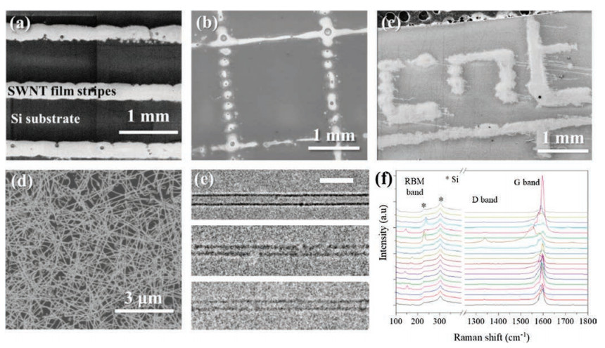
We chose water solutions of cobalt acetate as the inks and printed them on hydrophilically modified Si substrates. Carbon nanotube films of various pattern, such as stripes, cross lines, and "cnt" letters were grown as designed, as shown by the scanning electron microscopy (SEM) images in Figs. 1a-d. When 0.1 mmol/L cobalt acetate ink was used, there was aggregated catalysts at the margins of the stripes (Fig. S1 in Supporting Information), which were very likely caused by the coffee ring effect. However, when the concentration of cobalt acetate ink was increased to 1 mmol/L, the distribution of SWNTs within stripes were uniform, as shown in Fig. S2 in Supporting Information. Patterned SWNT arrays were also grown on quartz substrates with this method. We transferred the nanotube films to TEM grids to determine the wall number of nanotubes. With high-resolution transmission electron microscopy (HRTEM), it was confirmed that most nanotubes grown were SWNTs. Three typical HRTEM images of the SWNTs were shown in Fig. 1e, with diameters of 2.8 nm, 2.3 nm, and 2.4 nm, respectively. Typical radial breathing mode (RBM) band of SWNTs appeared in Raman spectra (Fig. 1f), which was in agreement with the observation in HRTEM. The high G/D ratio in most Raman spectra indicated good quality of the SWNTs.

|
Download:
|
| Fig. 1. The SEM image of (a) SWNT film stripes, (b) cross lines, and (c) "cnt" letters on Si substrates. (d) A zoom-in SEM image of the SWNT film stripes. (e) HRTEM images of SWNTs. The scale bar is 10 nm. (f) Raman spectra taken from random positions in the SWNT films. | |
In the printing process, the patterning results were largely affected by the shape of the precursor droplets on substrates, which was generally determined by three factors: the interface tensions at the gas-solid, gas-liquid, and liquid-solid interfaces, denoted as γgs, γgl, and γls, respectively. In the equilibrium state, the three interface tensions follow the Young's equation:

|
where θ is the contact angle. When γgl or γls increases, which means the surface tension of the liquid increases or its affinity to the substrate surface decreases, the contact angle θ increases and the droplet tends to shrink. We measured contact angles of water and ethanol droplets (1 mmol/L cobalt acetate solution) on Si substrates with various surface properties: Si substrates treated with the so-called piranha solution (mixture of H2SO4 and 30% H2O2 in the volume ratio of 7:3), which was very hydrophilic; pristine Si substrates, whose hydrophilicity was in the middle; and Si substrates treated with diluted hydrofluoric acid, which was relatively hydrophobic. Optical images of those droplets were shown in Fig. 2 and the corresponding contact angles were listed in Table 1.

|
Download:
|
| Fig. 2. Optical images for contact angle measurements. The droplets in (a-c) were water inks and those in (d-f) were ethanol inks. The substrates were hydrophilic Si (a & d), pristine Si (b & e), and hydrophobic Si (c & f), respectively. | |
|
|
Table 1 Contact angles of ink droplets on various Si substrates. |

Ethanol ink droplets always had much smaller contact angles comparing to water ink droplets (Fig. 2 and Table 1). For example, on Si substrates treated with piranha solutions, the contact angle of the water ink droplet was 39° while that of the ethanol ink droplet was 5°. This was probably caused by the much smaller surface tension of ethanol as well as its greater affinity to the substrates. The surface tension of pure ethanol at 25 ℃ is 22.0 mN/m, which is only about 1/3 of the surface tension of water, which is 72.0 mN/m [29]. SWNT film stripes grown from ethanol inks on those substrates were significantly broader than those from water inks due to the bigger contacting area of the droplets caused by the smaller contact angle of ethanol (Figs. 2a and d). In addition, there were more holes in the stripes when ethanol was used, which was also likely caused by the smaller surface tension of ethanol. The holes were probably results of the remaining bubbles in the droplets, generated during the droplets ejected from the printer. The smaller surface tension of ethanol meant smaller interface energy increase when the interface of gas and liquid was enlarged by the presence of the bubbles, which made the bubbles more stable in ethanol droplets. Therefore, there were more holes appeared in the ethanol stripes.
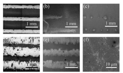
We then compared the patterning results on Si substrates with different surface properties. For both water and ethanol inks, the contact angles increased as the substrates changed from hydrophilic to hydrophobic, indicating the weaker affinity for the substrates (Fig. 2 and Table 1). For water inks, the SWNT films retained the shape of stripes best on the hydrophilic substrates (Figs. 3a-c). As the substrate became more and more hydrophobic, it became harder for the droplets to retain in the shape of a long stripe because of the increasing contact angle, and thus the SWNT films changed from stripes to dots. Similar phenomena were also observed for ethanol inks (Figs. 3d-f). However, on pristine Si substrates, the SWNT films grown from ethanol inks were still in stripe shape, which was probably because of the smaller contact angle of ethanol droplets.

|
Download:
|
| Fig. 3. SWNT film stripes grown from water inks on (a) hydrophilic, (b) pristine, and (c) hydrophobic Si substrates, and from ethanol inks on (d) hydrophilic, (e) pristine, and (f) hydrophobic Si substrates, respectively. | |
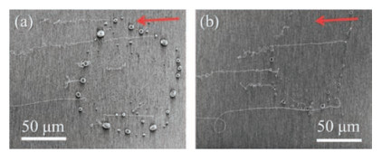
In addition to patterning the catalyst precursors, the inkjet printing patterning method was also used to pattern catalyst supports for SWNT growth. In our previous work [30, 31], we found that Cu tended to vaporize and renucleate at positions with rough surfaces. Utilizing this property, we patterned cerium oxide particles on Si substrates by the inkjet printing and grew SWNTs with Cu catalysts deposited (Fig. 4). The surfaces of cerium oxide particles were much rougher than the Si substrate, which led to the preferred nucleation of Cu vapor on the cerium oxide particles. As Fig. 4 showed, almost all SWNTs were grown from the cerium oxide particles.

|
Download:
|
| Fig. 4. SEM images of SWNTs grown from patterned cerium oxide particles. The arrows indicated the direction of gas flow. | |
In summary, we demonstrated that inkjet printing is feasible to patterning catalysts for the growth of SWNTs. Metal salt solutions were printed on substrates with a regular office-use printer to grow SWNTs in various patterns. The solvents of the ink solutions and their affinities to the substrates had significant influence on the patterning results. Challenges for this patterning method mainly lie in improving resolution and uniformity, which requires better control of the size and pattern of ink droplets and distribution of the catalysts. Properties of the inks and the substrates, such as surface tension, volatility, and viscosity of the inks and the surface properties of the substrates are the key factors for patterning. Our research reveals the potential of inkjet printing in catalyst patterning. With the great simplicity and flexibility, we believe inkjet printing will find broad applications in preparing functional material patterns.
AcknowledgmentsThis research is financially supported by Ministry of Science and Technology of the People's Republic of China (No. 2016YFA0201904), the National Natural Science Foundation of China (Nos. 21631002, U1632119 and 91333105).
Appendix A. Supplementary dataSupplementary material related to this article can be found, in the online version, at doi:https://doi.org/10.1016/j.cclet.2018.06.008.
| [1] |
P. Avouris, Z. Chen, V. Perebeinos, Nat. Nanotechnol. 2 (2007) 605-615. DOI:10.1038/nnano.2007.300 |
| [2] |
A.D. Franklin, Nature 498 (2013) 443. DOI:10.1038/498443a |
| [3] |
A.D. Franklin, Science 349 (2015) 704-715. |
| [4] |
M.M. Shulaker, G. Hills, N. Patil, et al., Nature 501 (2013) 526. DOI:10.1038/nature12502 |
| [5] |
Z. Zhang, L. Wei, X. Qin, Y. Li, Nano Energy 15 (2015) 490-522. DOI:10.1016/j.nanoen.2015.04.003 |
| [6] |
L. Yu, C. Shearer, J. Shapter, Chem. Rev. 116 (2016) 13413-13453. DOI:10.1021/acs.chemrev.6b00179 |
| [7] |
J. Wang, Electroanalysis 17 (2005) 7-14. |
| [8] |
M.F.L. De Volder, S.H. Tawfick, R.H. Baughman, A.J. Hart, Science 339 (2013) 535-539. DOI:10.1126/science.1222453 |
| [9] |
F. Lu, L. Gu, M.J. Meziani, et al., Adv. Mater. 21 (2009) 139-152. DOI:10.1002/adma.v21:2 |
| [10] |
N.R. Franklin, Y. Li, R.J. Chen, et al., Appl. Phys. Lett. 79 (2001) 4571. DOI:10.1063/1.1429294 |
| [11] |
S. Huang, B. Maynor, X. Cai, J. Liu, Adv. Mater. 15 (2003) 1651-1655. |
| [12] |
S.J. Kang, C. Kocabas, T. Ozel, et al., Nat. Nanotechnol. 2 (2007) 230. DOI:10.1038/nnano.2007.77 |
| [13] |
R. Xiang, T. Wu, E. Einarsson, et al., J. Am. Chem. Soc. 131 (2009) 10344-10345. DOI:10.1021/ja902904v |
| [14] |
A. Javey, H. Dai, J. Am. Chem. Soc. 127 (2005) 11942-11943. DOI:10.1021/ja0536668 |
| [15] |
L. Ding, W. Zhou, H. Chu, et al., Chem. Mater. 18 (2006) 4109-4114. DOI:10.1021/cm061122e |
| [16] |
W. Zhou, C. Rutherglen, P. Burke, Nano Res. 1 (2008) 158-165. DOI:10.1007/s12274-008-8012-9 |
| [17] |
L. Ding, C. Li, W. Zhou, et al., Eur. J. Inorg. Chem. (2010) 4357-4362. |
| [18] |
M. He, X. Ling, J. Zhang, Z. Liu, J. Phys. Chem. B 109 (2005) 10946-10951. DOI:10.1021/jp051127j |
| [19] |
B. Li, C.F. Goh, X. Zhou, et al., Adv. Mater. 20 (2008) 4873-4878. DOI:10.1002/adma.v20:24 |
| [20] |
I. Kuljanishvili, D.A. Dikin, S. Rozhok, et al., Small 5 (2009) 2523-2527. DOI:10.1002/smll.v5:22 |
| [21] |
R. Parashkov, E. Becker, T. Riedl, et al., Proc. IEEE 93 (2005) 1321-1329. DOI:10.1109/JPROC.2005.850304 |
| [22] |
E. Tekin, P.J. Smith, U.S. Schubert, Soft Matter 4 (2008) 703-713. DOI:10.1039/b711984d |
| [23] |
M. Singh, H.M. Haverinen, P. Dhagat, G.E. Jabbour, Adv. Mater. 22 (2010) 673-685. DOI:10.1002/adma.v22:6 |
| [24] |
J. Kim, R. Kumar, A.J. Bandodkar, J. Wang, Adv. Electro. Mater. 3 (2017) 1600260. DOI:10.1002/aelm.201600260 |
| [25] |
H. Ago, K. Murata, M. Yumura, et al., Appl. Phys. Lett. 82 (2003) 811-813. DOI:10.1063/1.1540726 |
| [26] |
H. Tempel, R. Joshi, J.J. Schneider, Mater. Chem. Phys. 121 (2010) 178-183. DOI:10.1016/j.matchemphys.2010.01.029 |
| [27] |
M. Mansoor, I. Kinloch, B. Derby, Key Eng. Mater. 442 (2010) 7-14. DOI:10.4028/www.scientific.net/KEM.442 |
| [28] |
C. Chatzikomis, S. Pattinson, K.K. Koziol, I. Hutchings, J. Mater. Sci. 47 (2012) 5760-5765. DOI:10.1007/s10853-012-6467-2 |
| [29] |
D. R. Lide, CRC Handbook of Chemistry and Physics. 85th. ed.. Boca Raton: CRC Press, 2005: pp. 6-135.
|
| [30] |
R. Cui, Y. Zhang, J. Wang, et al., J. Phys. Chem. C 114 (2010) 15547-15552. DOI:10.1021/jp100286c |
| [31] |
X. Zhao, Y. Liu, R. Cui, Y. Li, Carbon 110 (2016) 390-395. DOI:10.1016/j.carbon.2016.09.036 |