 2018, Vol. 29


b Advanced Nano-materials Division, Key Laboratory of Nano-Devices and Applications, Suzhou Institute of Nano-Tech and Nano-Bionics, Chinese Academy of Sciences, Suzhou 215123, China
Flexibility is one of the most fascinating features of organic electronic devices such as organic field-effect transistors (OFETs), which mainly arises from the natural flexibility of organic semiconductors due to the weak intermolecular interaction [1-7]. This feature enables organic device to be highly promising for the flexible and wearable products [8-15]. In general, thinner film device has more flexibility that can easily fit on body or object surface with arbitrary geometry [16, 17]. In spite of the intrinsic flexibility of organic semiconductors, the construction of flexible organic devices, especially the thin devices, has encounter lots of technological challenges. Until now, flexible devices have mainly been achieved via two kinds of routes. In first approach, flexible devices can be directly constructed on thin polymer substrates by layer to layer patterning method [18-22]. However, commercialized polymer substrates usually have poor smoothness and thin polymer film trend to crimp, that is not good for follow-up process [22, 23].
The second method to fabricate flexible devices is to peel off the whole or part device from rigid substrates by using release layer with weak adhesive strength or a sacrificial layer [24-26]. The smooth rigid substrate, such as silicon wafer, provides a stable platform to fabricate smoother film on it compared to polymer substrate. In this method, thin organic field-effect transistors are firstly fabricated on either a sacrificial layer such as copper foil [27-29], polyvinyl alcohol (PVA) [30], poly(sodium-4-styrenesulf onate) (PSSNa) [31] layer or a release layer such as polyacrylonitrile (PAN) [32-35], and then the whole or part device are striped off the rigid substrate with specific etchant solution or penetrating solvent, which produces thin device floating on the liquid surface. However, the usage of etchants and excessive solvent greatly increases not only the risk of contamination and performance degradation, but the difficulty of transfer.
Herein, we develop a facile peel-off method to transfer thin film to various substrates. PAN film can be easily stripped off the silicon substrate by the penetration of water into the PAN/silicon interface. Notably, the peel off process only uses micro volume water that largely reduces the disadvantageous influence of excessive solvent in the reported methods [22-24]. The method simplifies steps for transferring the film. We further demonstrate technique to fabricate organic transistors on Si substrate and flexible PET film. Benefiting from the usage of trace water, the electrical performance before and after transfer remains at the same level.
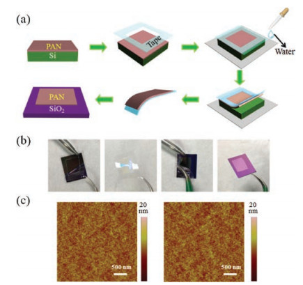
The schematic fabrication procedure of transferring ultra thin film is illustrated in Fig. 1a. First, an ultra thin and uniform PAN film (about 80-400 nm) is formed on a hydrophilic Si substrate by spin coating. Subsequently, we stick a single-sided adhesive tape frame (PET adhesive tape plays a supporting role) on the PAN film. After that, a little water is dripped nearby Si substrate. Under the assistance of the tape frame, PAN film can be easily peeled from the Si substrate to form a free-standing PAN film. Interestingly, the process uses only micro volume water as an assist that trends to penetrate into PAN/Silicon interface and therefore minimizes the interface adhesive strength during the peel off process. Owing to hydrophilic surfaces of Si substrate by O2 plasma, the little water tends to infiltrate into hydrophilic surface of Si substrate [36, 37]. And the trace water acts as a luvricant that helps with the peel off process. After the peel off process, the free-standing PAN film can be laminated on the other substrate spontaneously (such as SiO2, Si and PET). Then, the system was heat to 60 ℃ to remove the trace water, which also assists in peeling off the adhesive tape. Through the above processes, the PAN film can be transfer from silicon substrate to various substrate.

|
Download:
|
| Fig. 1. (a) The schematic diagram and (b) photograph of PAN film transfer. (c) AFM images before being transferred and after being transferred onto the Si. | |
Besides, thickness of thin PAN film can be modified by concentration. As shown in Fig. 1b, an ultrathin (85.2 nm) PAN film prepared via PAN/dichlorobenzene solution (20 mg/mL) is transferred to SiO2 substrate. Then we increased the concentration to 50 mg/mL and prepared 401.2 nm PAN film on Si substrate. After transferring to SiO2, thickness of thin PAN film becomes 397.7 nm, the slight difference of thickness may stem from the measurement errors. The transfer process slightly modify root-mean-square roughness (RMS) from 1.04 nm to 1.25 nm obtained by atomic force microscope (AFM) in Fig. 1c. These measurements indicate that PAN film is almost fully transferred and the transfer process well keeps the smoothness without forming cracks and wrinkles. Therefore, the ultrathin and flat film would be desirable to use as ultrathin substrate or dielectric layer to fabricate flexible full or partial device, such as OFET, OPV, OLED. It is worth noting that only about 10 mL water can achieve the transfer process for 1 cm2 area PAN film. Importantly, compared to water-floatation methodology, this method using little water as assistant has not only simplify transfer steps but drastically reduce risk that the active layers of devices contact with water.
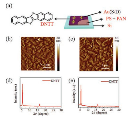
To testify the potential of our strategy to transfer thin organic transistors to various substrate, top-contact OFETs based on dinaphtho[2, 3-b:20, 30-f]thieno[3, 2-b]thiophene (DNTT) were fabricated (Fig. 2a) on a Si substrate. Here, we use Si as gate, PS and PAN polymer film as dielectric. The PS polymer film (thickness of 34 nm) was formed to improve interface properties and smoothness by spinning on PAN film (thickness of 350 nm) from 10 mg/mL toluene solution and annealing at 70 ℃ for 30 min. Next, 20 nm DNTT semiconductor is deposited on PS/PAN film at a rate of 0.05 Å/s by vacuum thermal evaporation. Then, source and drain electrodes of Au are deposited by shadow mask at a rate of 0.10 Å/s under 10-4 Pa by vacuum thermal evaporation. To characterize morphology of the surface, atomic force microscope (AFM) image of DNTT demonstrates a dendritic morphology that means good film quality on the dielectric layer of polystyrene (PS) and PAN (Fig. 2b). X-ray diffraction (XRD) pattern of the DNTT film reveals high crystalline on the dielectric layer shown as Fig. 2d.

|
Download:
|
| Fig. 2. (a) The schematic diagram AFM image of DNTT (b) after and (c) before being transferred. XRD patterns of DNTT (d) after and (e) before being transferred. | |
Then, the device was transferred to a new Si substrate through the peel-off process. AFM (Fig. 2c) and XRD (Fig. 2d) measurements are performed to characterize the morphology and crystalline of DNTT film again. The results indicate that the morphology and molecular ordering are not affected by the transfer process.
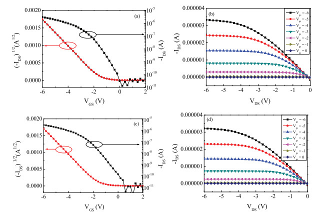
To further verify the influence of peel-off transfer method on the electrical performance of transistors, we measured the electrical properties of DNTT OFET on Si substrates before and after transfer. Typical p-type transfer and output characteristics are shown in Fig. 3, which display that the device can be operated under low voltage of 6 V (Figs. 3a and c), which mainly benefits from the small thickness of dielectric layer (384 nm) and high quality semiconductor layer. The low operating voltage is good for energy saving and safe for wearable device on body [21, 38-41]. The mobility of OTFT before and after transfer on a Si substrate is calculated to be 1.75 cm2 V-1 s-1 and 1.80 cm2 V-1 s-1, respectively. From images of Figs. 3a and c, we find threshold voltage (-1 V) and the mobility show negligible difference before and after the peel off process. Furthermore, the on/off ratio of remain keep 104 after transfer step. These results clearly confirm that PAN film is not only favorable for ultra thin OFET transfer, but also keeps good dielectric properties. More remarkably, our transfer method may well maintain the device performance which is highly useful for practical applications.

|
Download:
|
| Fig. 3. (a) Transfer and (b) output characteristics of the device before being transferred. (c) Transfer and (d) output characteristics of the device after being transferred onto the Si. | |
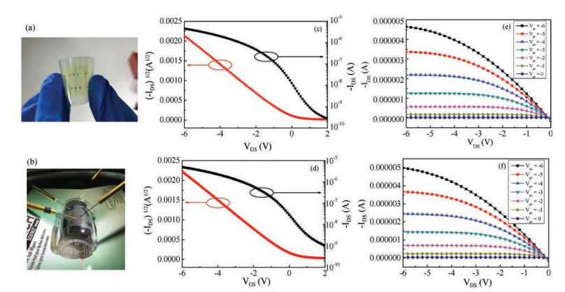
To fabricate flexible OFETs, the peeled PS/PAN film with DNTT semiconductor and source/drain electrodes is peel off from Si substrate with a tape. After the peel off process, the free-standing film can be transferred to flexible substrate, such as PET, PEN and PI. Figs. 4a and b show flexible OFETs that choose PET film as flexible substrate and ITO as gate electrode. As show in Fig. 4, we perform transfer and output characteristics, from which the fieldeffect mobility, threshold voltage and on/off ratio are calculated to be 1.73 cm2 V-1 s-1, 104, and 0 V, respectively. Then we make a test on the mechanical flexibility of the same device to demonstrate electrical stability upon bending. Here, the device is fixed on side wall of a 25 mL beaker that has 1.89 cm bending radius. It can be seen that the device shows good electrical properties upon bending. Notably, the field-effect mobility of device has not decrease, but slightly increases to 1.75 cm2 V-1 s-1. The threshold voltage (0 V) and on/off ratio (104) remain unchanged. The bending measurement indicates the PAN film is suitable for the OFETs with good performance.

|
Download:
|
| Fig. 4. (a) Photograph of OFETs on PET substrate and (b) bending test on a beaker. (c) Transfer and (e) output characteristics of the device before being transferred. (d) Transfer and (f) output characteristics of the device after being transferred onto the PET. | |
In conclusion, we developed a micro-volume water assisted transfer method to construct flexible organic transistors. In this strategy, PAN film can be easily peeled off with trace water and further transferred to various substrates. Using PAN as supporting and dielectric layers, high performance flexible organic transistors are fabricated. Remarkably, the method uses only micro volume water as a assist to peel off PAN film, which reduces the risk of contamination by solvent and thus greatly contributes to the performance maintenance. Benefiting from this feature, the performance of organic transistor remains the same level before and after transfer. A bending test further demonstrates the device exhibits good performance upon bending. Our peeling-off method is not limited to flexible OFETs, but also has the potential to be used ultra thin flexible OLED, OPV, and other electronic devices based on nanocarbon, 2D materials, nanowire, etc., which is thus highly promising for the construction of flexible electronic devices.
AcknowledgmentsThis study was financially supported by the Program for Special Appointment (Eastern Scholar) at Shanghai Institute of Higher Learning (No. 21577086), the National Natural Science Foundation of China (No. 21573277).
| [1] |
A.C. Arias, J.D. MacKenzie, I. McCulloch, J. Rivnay, A. Salleo, Chem. Rev. 110 (2010) 3-24. DOI:10.1021/cr900150b |
| [2] |
L. Zhang, C.A. Di, G. Yu, Y.Q. Liu, J. Mater. Chem. 20 (2010) 7059-7073. DOI:10.1039/c0jm00331j |
| [3] |
M. Uno, K. Nakayama, J. Soeda, et al., Adv. Mater. 23 (2011) 3047-3051. DOI:10.1002/adma.v23.27 |
| [4] |
C.D. Dimitrakopoulos, P.R.L. Malenfant, Adv. Mater. 14 (2002) 99-117. |
| [5] |
S.T. Bromley, M. Mas-Torrent, P. Hadley, C. Rovira, J. Am. Chem. Soc. 126 (2004) 6544-6545. DOI:10.1021/ja049762a |
| [6] |
W.L. Kalb, F. Meier, K. Mattenberger, B. Batlogg, Phys. Rev. B 76 (2007) 184112. DOI:10.1103/PhysRevB.76.184112 |
| [7] |
J.X. Dong, H.L. Zhang, Chin. Chem. Lett. 27 (2016) 1097-1104. DOI:10.1016/j.cclet.2016.05.005 |
| [8] |
T. Yokota, Y. Inoue, Y. Terakawa, et al., Natl. Acad. Sci. U.S.A. 112 (2015) 14533-14538. DOI:10.1073/pnas.1515650112 |
| [9] |
A. Chortos, J. Liu, Z.A. Bao, Nat. Mater. 15 (2016) 937-950. DOI:10.1038/nmat4671 |
| [10] |
T. Someya, Z. Bao, G.G. Malliaras, Nature 540 (2016) 379-385. DOI:10.1038/nature21004 |
| [11] |
T.Q. Trung, S. Ramasundaram, B.U. Hwang, N.E. Lee, Adv. Mater. 28 (2016) 502. DOI:10.1002/adma.v28.3 |
| [12] |
S.Y. Yeo, S. Park, Y.J. Yi, D.H. Kim, J.A. Lim, ACS Appl. Mater. Interface 9 (2017) 42996-43003. DOI:10.1021/acsami.7b15960 |
| [13] |
S.C.B. Mannsfeld, B.C.K. Tee, R.M. Stoltenberg, et al., Nat. Mater. 9 (2010) 859-864. DOI:10.1038/nmat2834 |
| [14] |
J. Xu, S.H. Wang, G.J.N. Wang, et al., Science 355 (2017) 59. DOI:10.1126/science.aah4496 |
| [15] |
M.X. Chen, Y. Yang, D.Z. Chen, H. Wang, Chin. Chem. Lett. 29 (2017) 564-570. |
| [16] |
J.W. Jeong, W.H. Yeo, A. Akhtar, et al., Adv. Mater. 25 (2013) 6839-6846. DOI:10.1002/adma.v25.47 |
| [17] |
C.Y. Li, X.P. Li, Y.T. Ma, et al., Chin. Chem. Lett. 16 (2005) 967-970. |
| [18] |
D.R. Hines, A. Southard, M.S. Fuhrer, J. Appl. Phys. 104 (2008) 024510. DOI:10.1063/1.2959821 |
| [19] |
T. Sekitani, U. Zschieschang, H. Klauk, T. Someya, Nat. Mater. 9 (2010) 1015-1022. DOI:10.1038/nmat2896 |
| [20] |
D.Y. Ji, L. Jiang, H.L. Dong, et al., ACS Appl. Mater. Interfaces 5 (2013) 2316-2319. DOI:10.1021/am302684k |
| [21] |
G. Grau, V. Subramanian, Adv. Electron. Mater. 2 (2016) 1500328. DOI:10.1002/aelm.201500328 |
| [22] |
E.K. Lee, C.H. Park, J. Lee, et al., Adv. Mater. 29 (2017) 1605282. DOI:10.1002/adma.201605282 |
| [23] |
H.T. Yi, M.M. Payne, J.E. Anthony, V. Podzorov, Nat. Commun. 3 (2012) 1259. DOI:10.1038/ncomms2263 |
| [24] |
W. Deng, X. Zhang, C. Gong, et al., J. Mater. Chem. C 2 (2014) 1314-1320. DOI:10.1039/C3TC31678E |
| [25] |
K. Fukuda, Y. Takeda, Y. Yoshimura, et al., Nat. Commun. 5 (2014) 4147. DOI:10.1038/ncomms5147 |
| [26] |
G.A. Salvatore, N. Munzenrieder, T. Kinkeldei, et al., Nat. Commun. 5 (2014) 2982. DOI:10.1038/ncomms3982 |
| [27] |
W. Deng, X. Zhang, H. Pan, et al., Sci. Rep. 4 (2014) 5358. |
| [28] |
Q. Shang, W. Deng, X. Zhang, et al., Adv. Electron. Mater. 2 (2016) 1600129. DOI:10.1002/aelm.201600129 |
| [29] |
J. Wang, X. Zhang, W. Deng, et al., Org. Electron. 34 (2016) 104-110. DOI:10.1016/j.orgel.2016.04.017 |
| [30] |
S.J. Noever, M. Eder, F. del Giudice, et al., Adv. Mater. 29 (2017) 1606283. DOI:10.1002/adma.v29.26 |
| [31] |
D. Ji, A.D. Donner, G. Wilde, W. Hu, H. Fuchs, RSC Adv. 5 (2015) 98288-98292. DOI:10.1039/C5RA21329K |
| [32] |
L. Zhang, C.A. Di, Y. Zhao, et al., Adv. Mater. 22 (2010) 3537-3541. DOI:10.1002/adma.201000123 |
| [33] |
L. Zhang, H. Wang, Y. Zhao, et al., Adv. Mater. 25 (2013) 5455-5460. DOI:10.1002/adma.201300675 |
| [34] |
H. Wang, H. Liu, Q. Zhao, et al., Adv. Mater. 28 (2016) 624-630. DOI:10.1002/adma.201503953 |
| [35] |
H. Wang, H. Liu, Q. Zhao, et al., Adv. Mater. 29 (2017) 1701772. DOI:10.1002/adma.201701772 |
| [36] |
T. Suni, K. Henttinen, I. Suni, J. Makinen, J. Electrochem. Soc. 149 (2002) G348-G351. DOI:10.1149/1.1477209 |
| [37] |
M.J. Perez-Roldan, D. Debarnot, F. Poncin-Epaillard, RSC Adv 4 (2014) 31409-31415. DOI:10.1039/C4RA05691D |
| [38] |
K. Takei, T. Takahashi, J.C. Ho, et al., Nat. Mater. 9 (2010) 821-826. DOI:10.1038/nmat2835 |
| [39] |
U. Zschieschang, F. Ante, T. Yamamoto, et al., Adv. Mater. 22 (2010) 982-985. DOI:10.1002/adma.200902740 |
| [40] |
S.J. Guo, Z.W. Wang, Z.Y. Xu, et al., Chin. Chem. Lett. 28 (2017) 2143-2146. DOI:10.1016/j.cclet.2017.08.041 |
| [41] |
W.H. Zhang, B.J. Jiang, P. Yang, Chin. Chem. Lett. 27 (2016) 1339-1344. DOI:10.1016/j.cclet.2016.06.044 |