 2018, Vol. 29


b School of Civil Engineering, Chongqing Institute of Engineering, Chongqing 400054, China;
c Technical Institute of Physics and Chemistry, Chinese Academy of Sciences, Beijing 100190, China
Zinc oxide (ZnO) is an important semiconductor metal oxide with a wide direct band gap of 3.37 eV at room temperature [1]. It has stimulated great research interest over the past few years due to its unique properties that are useful for the fabrication of nanolasers, optoelectronic devices, and photocatalysts [2]. As is well-known, the physical and chemical properties of materials are strongly depended on their size, size distribution, structures, and dimensions. In our previous works, we reported the control synthesis of semiconductor metal oxide using different methods [3-11]. Controllable preparation of well crystallized and novel morphological ZnO micro/nanostructures is highly desired for many applications. Considerable effort has been devoted to the morphology-controllable synthesis of ZnO or ZnO-based microstructures [12-21]. For example, Qin et al. synthesized ZnO microstructures with hexagonal disk, prismoid, prism and pyramid via a facile two-step low temperature hydrothermal reaction [15]. Li and Wang prepared ZnO hierarchical microstructures with uniform flower-like morphology through a template- and surfactant-free aqueous solution route [16]. Cao et al. took advantage of a modified solvothermal route to achieve deliberate size modulation of ZnO nanorods [17]. Liu et al. synthesized 3D ZnO tubular flowerlike architectures and radial nanorods in the presence of polyethylene glycol [18]. Oh and co-workers prepared micrometersized ZnO hexagonal rings using the coordination-polymer template-directed approach [19]. Zhang et al. reported the shape-selective synthesis of ZnO particles with distinctive shapes by a novel polyvinylpyrrolidone-directed crystallization route [20]. Although many strategies have been developed to construct ZnO or ZnO-based microstructures, it is not easy to achieve good control of a ZnO structure with the desired crystal planes, morphologies, and microstructures. Thus, further research and designing new ZnO architectures through a facile aqueous solution route is necessary.
Herein, we propose a facile route for fabricating ZnO hexagonal bilayer disk-like microstructures (HBDMs) via a solvothermal method in the presence of polyvinylpyrrolidone (PVP). UV-vis spectrum reveals that ZnO sampls show an appreciable red shift and the band gap energy of the obtained ZnO samples were about 3.15 eV. A very strong ultraviolet (UV) emission at the UV region was observed in the photoluminescence (PL) spectrum of the asprepared ZnO samples tested at room-temperature. These ZnO HBDMs may offer new opportunities for the development of electronics, optics and gas sensing applications
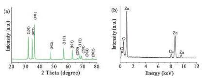
The ZnO HBDMs were prepared through a solvothermal method in the presence of PVP. The structure, morphology, and optical properties of the as-prepared samples were investigated by X-ray diffraction (XRD), scanning electron microscopy (SEM), UV-vis and PL spectrophotometer. Fig. 1a shows the typical XRD patterns of the as-prepared ZnO HBDMs. The ZnO powders displayed a good crystallinity and can be assigned to the wurtzite hexagonal ZnO structure (JCPDS No. 36-1451). Energy-dispersive X-ray spectroscopy (EDX) result shown in Fig. 1b reveals that the as-prepared sample contains Zn and O elements, and the atomic ratio of Zn/O is about 1:1.

|
Download:
|
| Fig. 1. XRD (a) and EDS (b) patterns of the ZnO HBDMs. | |
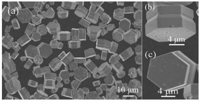
The general morphologies of the as-synthesized ZnO microstructures are shown in Fig. 2a. Many HBDMs can be observed. An individual ZnO hexagonal bilayer disk is shown in Figs. 2b and c. The hexagonal bilayer disk-like assembles consist of two uniform and smooth disks with an average edge length of 6 μm and thickness of ~4 μm.

|
Download:
|
| Fig. 2. Low-magnification SEM images of the ZnO HBDMs (a), SEM image of a single ZnO HBDM at various angles: (b) declivitous, (c) left-oblique. | |
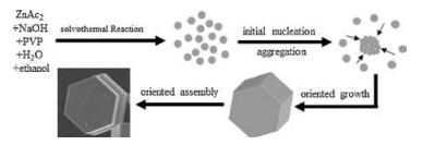
On the basis of previous studies [2, 18-25] and the above results, the possible growth processes of the ZnO HBDMs can be schematically illustrated, as shown in Fig. 3. First, numerous ZnAc2 was hydrolyzed in the highly basic reaction solution, and Zn(OH)42- ions were first formed. Then, under solvothermal conditions, a large number of tiny ZnO nanoparticles spontaneously appeared from the dehydration of Zn(OH)42- ions by initial homogeneous nucleation. The freshly crystalline nanoparticles are unstable and have a tendency to aggregate together and developed into larger crystals, as shown in Fig. S1 (Supporting informatiom), which may be driven by the minimization of interfacial energy. As we know, PVP is a typical nonionic surfactant. In the presence of certain amount of PVP, an intense coordination occurs between -C=O of PVP and Zn atom of ZnO, due to the O atom in the -C=O functional group of PVP has a negative charge and the Zn in the precursor particles is positively charged. As the reaction proceeded, some active sites on the surface of the initially formed ZnO aggregations would grow along the oriented direction and form a hexagonal disk-like microstructure (Fig. S1). Afterward, the formed hexagonal disk-like microstructures further oriented assembly to form ZnO HBDMs. Such a process was also observed in the synthesis of ZnO particles with distinctive shapes [20]. As Zhang and co-workers believed it is the dependence on the amount of surfactant in the reaction that makes the controllable nucleation and growth of ZnO possible, thus affording size control of the final product [20]. Here, PVP played the template-directed crystallization role [20]. The exact mechanism for the formation of the final samples need be further investigated.

|
Download:
|
| Fig. 3. Schematic illustration of the growth process of the ZnO HBDMs. | |
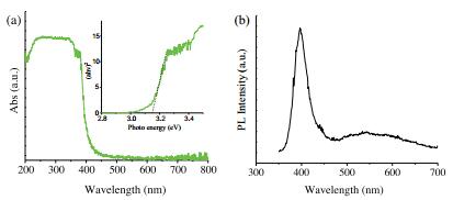
Fig. 4a shows the diffuse reflectance spectrum of the ZnO HBDMs. The inset in Fig. 4 shows the (αhν)2 versus photon energy hn curve for the ZnO samples. The band gap energy (Eg values) of the ZnO samples by extrapolating the straight portion of (αhν)2 against hν plot to the point α = 0, which is 3.15 eV for the ZnO HBDMs. The Eg value was a little different from the theoretic value (3.37 eV) [1], which could be connected with the distinctive shape and structure. Fig. 4b shows the room temperature PL spectrum of the as-prepared ZnO HBDMs. It can be observed that the PL spectrum consists of two characteristic parts, that is, a narrow and sharp peak located at the UV region and a broad spectral band falling into the region between 480 nm and 620 nm. According to the literature [26, 27], the near-band-edge UV emission typically results from the recombination of free or bound excitons through exciton-exciton collision [26]. The deep-level visible emission should be attributed to the presence of various point defects, such as an oxygen vacancy [28, 29]. Besides, the distinctive contrast between the strong UV band edge emission and weak green emission indicates that the as-prepared ZnO crystals have high crystallinity [30], which is consistent with the XRD result.

|
Download:
|
| Fig. 4. UV-vis diffuse reflectance spectrum (a) and PL spectrum (b) of the ZnO HBDMs. Inset: The (αhν)2-hν curve for the samples. | |
In summary, ZnO HBDMs with high crystallinity are successfully fabricated using a simple solvothermal method assisted with surfactant. UV-vis spectrum reveals that ZnO sampls show an appreciable red shift and the band gap energy of the obtained ZnO samples were about 3.15 eV. The PL spectrum consists of two characteristic parts, that is, a narrow and sharp peak located at the UV region and a broad spectral band falling into the region between 480 nm and 620 nm. The PL spectrum indicated that the existence of the recombination of free or bound excitons were responsible for the near-band-edge UV emission in the ZnO HBDMs. We believe these ZnO HBDMs will offer new opportunities for the development of electronics, optics and gas sensing applications.
AcknowledgmentsThis work was supported by the Shanghai Municipal Natural Science Foundation (Nos. 17ZR1411000, 14ZR1417100), and the Key Subject of Shanghai Polytechnic University (No. 4: Material Science and Engineering, XXKZD1601).
Appendix A. Supplementary dataSupplementary data associated with this article can be found, in the online version, at https://doi.org/10.1016/j.cclet.2017.12.018.
| [1] |
M.H. Huang, S. Mao, H. Feick, et al., Science 292 (2001) 1897-1899. DOI:10.1126/science.1060367 |
| [2] |
C. Jagadish, S. J. Pearton, Zinc Oxide Bulk, Thin Films and Nanostructures, Elsevier, New York, 2006.
|
| [3] |
L.P. Zhu, N.C. Bing, L.L. Wang, et al., Dalton. Trans. 41 (2012) 2959-2965. DOI:10.1039/c2dt11822j |
| [4] |
L.P. Zhu, G.H. Liao, N.C. Bing, et al., Mater. Lett. 65 (2011) 1287-1290. DOI:10.1016/j.matlet.2011.01.053 |
| [5] |
L.P. Zhu, G.H. Liao, N.C. Bing, et al., CrystEngComm 12 (2010) 3791-3796. DOI:10.1039/c0ce00038h |
| [6] |
L.P. Zhu, H.M. Xiao, W.D. Zhang, et al., Cryst. Growth Des. 8 (2008) 1113-1118. DOI:10.1021/cg701036k |
| [7] |
L.P. Zhu, W.D. Zhang, H.M. Xiao, et al., J. Phys. Chem. C 112 (2008) 10073-10077. DOI:10.1021/jp8019182 |
| [8] |
L.P. Zhu, W.D. Zhang, H.M. Xiao, et al., Cryst. Growth Des. 8 (2008) 957-961. DOI:10.1021/cg700861a |
| [9] |
L.P. Zhu, G.H. Liao, N.C. Bing, et al., J. Solid State Chem. 184 (2011) 2405-2409. DOI:10.1016/j.jssc.2011.07.013 |
| [10] |
L.P. Zhu, L.L. Wang, N.C. Bing, et al., Mater. Lett. 88 (2012) 164-167. DOI:10.1016/j.matlet.2012.06.105 |
| [11] |
L.P. Zhu, L.L. Wang, N.C. Bing, et al., ACS Appl. Mater. Interfaces 5 (2013) 12478-12487. DOI:10.1021/am403720r |
| [12] |
V. Arabali, M. Ebrahimi, H. Karimi-Maleh, Chin. Chem. Lett. 27 (2016) 779-782. DOI:10.1016/j.cclet.2016.01.026 |
| [13] |
F. Teng, L. Zheng, K. Hu, et al., J. Mater. Chem. C 4 (2016) 8416-8421. DOI:10.1039/C6TC02901A |
| [14] |
B. Zhao, F. Wang, H. Chen, et al., Adv. Funct. Mater. 27 (2017) 1700264-1700271. DOI:10.1002/adfm.v27.17 |
| [15] |
N. Qin, Q. Xiang, H. Zhao, et al., CrystEngComm 16 (2014) 7062-7073. DOI:10.1039/C4CE00637B |
| [16] |
B. Li, Y. Wang, J. Phys. Chem. C 114 (2010) 890-896. DOI:10.1021/jp909478q |
| [17] |
X. Cao, N. Wang, L. Wang, Nanotechnology 21 (2010) 065603. DOI:10.1088/0957-4484/21/6/065603 |
| [18] |
J. Liu, X. Huang, Y. Li, et al., Scr. Mater. 55 (2006) 795-798. DOI:10.1016/j.scriptamat.2006.07.010 |
| [19] |
S. Jung, W. Cho, H.J. Lee, M. Oh, Angew. Chem. Int. Ed. 48 (2009) 1459-1462. DOI:10.1002/anie.v48:8 |
| [20] |
J. Zhang, H. Liu, Z. Wang, et al., Adv. Funct. Mater. 17 (2007) 3897-3905. DOI:10.1002/(ISSN)1616-3028 |
| [21] |
S.H. Ko, D. Lee, H.W. Kang, Nano Lett. 11 (2011) 666-671. DOI:10.1021/nl1037962 |
| [22] |
X. Liu, Angew Chem. Int. Ed. 48 (2009) 2-6. DOI:10.1002/anie.200890277 |
| [23] |
Y. Sun, J. Hu, N. Wang, et al., New J. Chem. 34 (2010) 732-737. DOI:10.1039/b9nj00708c |
| [24] |
Q. Zhou, W. Chen, S. Peng, W. Zeng, The Sci. World J. 489170 (2014) 1-8. |
| [25] |
Y.X. Yin, L.Y. Jiang, L.J. Wan, et al., Nanoscale 3 (2011) 1802-1806. DOI:10.1039/c0nr00843e |
| [26] |
V.A. Fonoberov, K.A. Alim, A.A. Balandin, et al., Phys. Rev. B 73 (2006) 165317-165321. DOI:10.1103/PhysRevB.73.165317 |
| [27] |
R. Dingle, Phys. Rev. Lett. 23 (1969) 579-581. DOI:10.1103/PhysRevLett.23.579 |
| [28] |
B.Q. Cao, W.P. Cai, Y. Li, et al., Nanotechnology 16 (2005) 1734-1738. DOI:10.1088/0957-4484/16/9/054 |
| [29] |
S.J. Chen, Y.C. Liu, C.L. Shao, et al., Adv. Mater. 17 (2005) 586-590. DOI:10.1002/(ISSN)1521-4095 |
| [30] |
Y. Zhang, A. Mascarenhas, Phys. Rev. B 59 (1999) 2040-2044. DOI:10.1103/PhysRevB.59.2040 |