 2018, Vol. 29


Perovskite solar cells (PSCs) based on organic-inorganic hybrid lead trihalide perovskites have recently exhibited great potential of producing low cost solar electricity. The power conversion efficiency (PCE) of PSC has been skyrocketed from the initial 3.8% in 2009 [1] to current 22.7% [2] within 7 years. Compared to other types of solar cells, PSCs have advantages of low material and fabrication cost, outstanding photoelectric properties and remarkable PCE achieved with cost-effective solution processing method. Nevertheless, stability is the key issue for this type of solar cells that restricts their commercialization in practice [3-6].
Generally, a PSC has a sandwich configuration consisting of multiple layers of thin solid films including electron transport layer (ETL), perovskite based light harvesting layer and hole transport layer (HTL). There are several factors that affect the stability of PSCs. Except the factors on perovskite layer itself, such as crystal structure [7], surface morphology [8] and material composition [5], ion migration [9] at interface between different layers can also cause instability of PSC. In addition, erosion from air is another factor. Since perovskite materials are sensitive to moisture and oxygen, decomposition of device mainly occurs at the area where perovskite film is directly exposed to air. Therefore, HTMs not only play the role of extraction of hole from the perovskite light absorber and hole transportation, but also protecting the perovskite film from directly contacting with the metal electrode [10] and air [11], retarding degradation. Up to now, organic p-type semiconductors are widely used as HTMs in PSCs, such as small organic molecules [12-15], conducting polymers [16] and organometallic compounds [17], which show impressive performance in terms of PCE compared with other kinds of HTMs. Nonetheless the durability of the device using organic HTMs is generally unsatisfactory. HTMs based on different organic p-type semiconductors for PSCs have been well reviewed by Laura and coworkers [18]. They have suggested employing hydrophobic dopants or adjusting chemical structure of organic HTMs to cope with the issue of instability and hysteresis behaviour of PSCs. Compared to organic HTMs, inorganic p-type materials and carbon materials have also demonstrated the great potential as HTL of PSCs for application in reality owing to inherent long-term material stability and low cost. Although review of inorganic HTM and carbon materials have been reported before, given the rapid progress of this active research field, it is essential to retrospect and update the pioneers'works on inorganic HTMs and carbon materials for PSCs.
In this review, we mainly focus on HTMs based on inorganic ptype semiconductors and carbon materials for PSCs. The review is composed of the following sections. Firstly, a section of brief introduction of device structure and the requirements of ideal HTMs for PSCs is provided. This is followed by research progress on inorganic p-type semiconductors such as NiOx, CuSCN, CuOx, V2O5, CuS and MoO2. After this, the application of various type of carbon materials including SWCNTs, MWCNTs, GO and functionalized carbon materials as HTMs for PSCs is summarized. Finally, a conclusion and outlook for the future research on HTMs for PSC is presented.
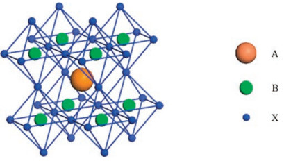
2. Device structure and requirements of HTMsPerovskite materials can be denoted by a general chemical formula of ABX3 [19] with structure shown in Fig. 1. In regard to crystal structure for PV application, cubic crystal structure is preferred for organic-inorganic lead trihalide perovskite materials in PSCs. Specifically, A and B represent cations with various atomic radii (A is bigger than B), whereas X is an anion. B are metallic cation from Group Ⅳ (typically, Pb2+ or Sn2+) and X is normally halide anion (Cl-, Br-, or I-). These two different ions consist of corner sharing BX6 octahedra. A is usually monovalent organic cation, such as methylammonium (CH3NH3+) or formamidinium ((NH2)2CH+) occupying the space of the octahedral interstice [20]. The variation of A, B and X ions can accomplish tailoring of band position and bandgap of the perovskite, thereby affecting the optical and electrical properties of the material. The bandgap of perovskite materials can be tuned in the range of 1.10–2.88 eV which can be measured by UV–vis spectrometer and incident photon-to-electron efficiency (IPCE) spectrum [21-24]. It has been found that replacing CH3NH3+ (MA) with (NH2)2CH+ (FA) reduces the bandgap by around 0.07 eV while light absorption wavelength is extended by 40 nm at the same time [25]. Moreover, partial substitute of Pb2+ with Sn2+ can decrease the bandgap from 1.55 eV to 1.17 eV [26].

|
Download:
|
| Fig. 1. Crystal structure of cubic metal halide perovskites. A: Organic cation, B: Metallic cation and X: Halide anion. | |
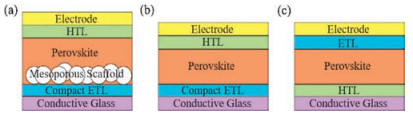
In terms of device structure, two main types of architectures have been developed with PSCs: a mesoscopic structure and a planar structure. Both device structures contain several stacking layers consisting of FTO substrate/n-type semiconductor layer/ perovskite/p-type semiconductor layer/metal electrode. As the first perovskite-based solar cells was originally derived from dye sensitized solar cells where n-type TiO2 and perovskite nanocrystals were employed as mesoporous layer and sensitizer respectively, the mesoscopic nanostructure has been widely used in the early stage of PSCs research [1]. As shown in Fig. 2a of a typical PSC, an ultrathin (20–50 nm) and dense electron transport layer is sandwiched between the transparent conducting oxide coated glass substrates (usually fluorine-doped tin oxide (FTO) coated glass) and a mesoporous metal oxide scaffold [27]. According to literatures, n-type TiO2, ZnO or insulating dielectric metal oxide, such as Al2O3 [28] can serve as the scaffold materials. The role of this mesoscopic scaffold is to assist the formation of a homogeneous perovskite film and to improve the electron transfer as well [29]. In the mesoporous structure, the perovskite is partially infiltrated into the mesoporous scaffold. About 100–300 nm hole-transporting material is deposited on top of the perovskite layer. The device is finished with a layer of electrical contact which is often based on gold or silver. The architecture of planar PSC is exhibited in Fig. 2b. The structure of the device is similar to that of mesoscopic architecture except that the mesoporous scaffold layer is completely excluded. The intrinsic perovskite layer (i layer) in this device structure is required to be flat and compact between electron extraction layer (n-type) and HTM layer (p-type) to form n-i-p planar heterojunction. Furthermore, PSC with inverted p-i-n planar configuration [20] (Fig. 2c) has also been demonstrated where the HTM layer is placed underneath the perovskite film but ETM layer is coated on the perovskite surface. For this type of PSCs, upon light illumination, photons pass through FTO and HTM before being absorbed by perovskite layer to generate electron-hole pairs. Because of energy band alignment, the photon-generated electrons are injected to the ETM. In the meantime, the photo-generated holes are transferred to the HTM. The holes and electrons are then collected through the current collector of FTO glass and metal electrode, respectively [30, 31].

|
Download:
|
| Fig. 2. Device architecture of (a) mesoscopic, (b) planar heterojunction and (c) inverted planar heterojunction perovskite solar cells. | |
In order to obtain stable PSCs with high performance, ideally a suitable HTM needs to meet several indispensable requirements. (1) The highest occupied molecular orbital (HOMO) energy level of the HTMs ought to be located higher than the valence band energy of perovskite. The open circuit voltage of the devices is increased if the energy offset between the HOMO level of HTMs and valence band of perovskite is minimum [18]. (2) Availability of good materials processibility for HTMs to form thin solid film by solution process or vapour deposition method. (3) An outstanding p-type semiconductor material should possess high hole-mobility (possibly, more than 10-3 cm2 V-1 s-1) to ensure rapid hole transportation rate, reduce recombination and series resistance, and increase the fill factor (FF) as well [32]. (4) The fabricated HTM should possess a compact, homogeneous and flat morphology to reduce charge recombination at interface. (5) Transparency in the visible spectra could be also necessary for HTMs used in PSC with inverted structure to reduce light absorption by the HTMs [33].
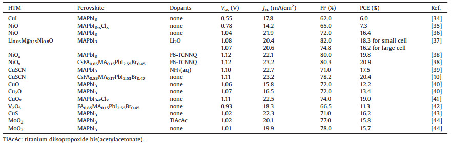
3. Inorganic hole transport materials for perovskite solar cellsInorganic p-type semiconductor materials are promising holetransporting materials to replace the organic HTMs currently used in PSCs owing to their advantages of intrinsically better long-term stability, high hole mobility and low cost fabrication [32]. Ideal inorganic HTMs for PSCs should have some characteristics, including appropriate valence band (VB) level whichmatches well with that of perovskite layer, higher hole mobility, good transparency in the range of visible to IR range, as well as good optical, thermal and chemical stability. Hither to, different inorganic HTMs have already been explored in PSCs. Table 1 illustrates the PCE of PSCs using various inorganic HTMs with efficiency varying from 6% [34] to nearly 20% [10]. Particularly, some inorganic materials, such as NiOx, CuOx and CuSCN have demonstrated the potential to replace the classic organic HTMs such as spiro-OMeTAD for PSCs. The energy levels of these inorganic HTMs are summarized in Fig. 3. The energy band level of perovskite materials that are most widely investigated are also shown. Clearly, the energy levels of these inorganic HTMs match very well with the valence band and conduction band (CB) of the perovskite, enabling hole separation while electron transport is blocked. The detailed research progress of some inorganic HTMs is shown in the following.

|
Download:
|
| Fig. 3. Schematic illustration of the energetic positions of mostly used components in PSCs, including ETMs, perovskite and various inorganic HTMs. | |
|
|
Table 1 Photovoltaic properties of perovskite solar cells based on inorganic hole transport materials. |
3.1. NiO
Nickel oxide (NiO) is a cubic wide-bandgap p-type material [45], which has been widely used as a HTM in DSSC and OPV devices. As is shown in Fig. 3, the valence band of NiO is located at -5.4 eV, which is very close to that of perovskite. It means the photo-generated holes at perovskite film can be injected into holetransporting layer effectively. NiO usually hybrids with Ni3+, therefore it is also denoted as NiOx in literature [46]. In 2014, Sarkar et al. [35] employed elecrodeposition to deposit NiO layer in an inverted planar structure PSC and obtained a PCE of 7.30%. After being annealed, the NiO layer was treated with UV-ozone and O2 plasma to further improve the photovoltaic properties. In 2016, Seo et al. [36] prepared ultrathin pure NiO film without any pinholes by the atomic layer deposition (ALD) method and achieved an optimum power conversion efficiency of 16.4%. This new technique can precisely control the NiO film thickness to obtain highly uniform and compact ultrathin layers through a unique growth mechanism at room temperature. Liyuan Han's group [37] used Li, Mg-codoped NiO (Li0.05Mg0.15Ni0.8O) as HTM, achieving a high PCE of 18.4%. The structure and the band scheme of the whole PSC are presented in Fig. 4. At the same time, PSC with large active area (>1 cm2) with an efficiency of 16.2% was also successfully prepared by this p-doped method, demonstrating the potential of NiO as an efficient HTM for PSCs. The shortcoming of NiO as HTM is that FF and Voc of the cells are generally lower than the classical organic HTMs, particularly, when the NiO layer is deposited by solution process. Most recently, Wei and co-workers [38] used 2, 2'- (perfluoronaphthalene-2, 6-diylidene)dimalononitrile (F6TCNNQ) solution to treat NiOx layer to develop a novel molecule-doped nickel oxide as HTM for planar inverted PSCs. After F6TCNNQ treatment, the energy level offset between the valence band maximum (VBM) of NiOx and perovskite decreased to 0.04 eV, which is conducive to charge transfer. As a result, the considerable PCEs of 20.9% and 19.8% for CsFAMA triple cation and MAPbI3 based PSCs were achieved, respectively.

|
Download:
|
| Fig. 4. Structure and band alignments of the PSC. (A) Diagram of the cell configuration highlighting the doped charge carrier extraction layers. The right panels show the composition of Ti(Nb)Ox and the crystal structure of Li+-doped NixMg1–xO, denoted as NiMg(Li)O. (B) A high-resolution crosssectional SEM image of a complete solar cell. (C) Band alignments of the solar cell. Reprinted with permission [37]. Copyright 2015, American Association for the Advancement of Science. | |
3.2. CuSCN
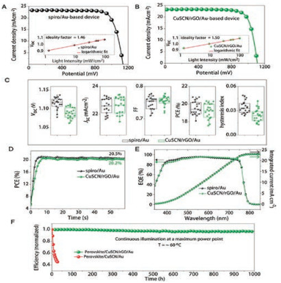
Recently, copper thiocyanate (CuSCN) appears to be a promising choice of inorganic HTMs because of its wide bandgap (Fig. 3), high mobility and transparency in the visible and infrared regions [47, 48]. The ultrathin (3–5 nm) CuSCN layers can be made via spin-casting aqueous CuSCN-ammine complex solution as reported by Wijeyasinghe et al. [39] In accordance with the results from field-effect transistor, the aqueousprocessed CuSCN film displayed an extraordinary hole mobility approaching 0.1 cm2 V-1 s-1, which is approximately five-fold higher than the organic HTM layer. An impressive PCE of 17.5% for planar PSC based on aqueous-processed CuSCN HTM was reached. Furthermore, in 2017, Grätzel's group [10] utilized fast solvent removal method to generate dense and highly conformal CuSCN layer. The corresponding PSCs yielded stabilized efficiency more than 20% (Fig. 5). The PSCs also showed high thermal stability under long-term heating. Especially, incorporation of a conductive reduced graphene oxide spacer layer between the CuSCN and gold significantly enhanced device stability without reducing efficiency. The devices still remained >95% of their original efficiency even after aging at a maximum power point for 1000 h at 60 ℃. They found that the instability of PSCs derives from the degradation of CuSCN/gold interface instead of the interface between perovskite and CuSCN. However, a significant problem associated with CuSCN is that most of the solvents which can dissolve it can also degrade the perovskite film [49].

|
Download:
|
| Fig. 5. Photovoltaic characterization of devices based on spiro-OMeTAD and CuSCN hole transporting layers. (A) J-V curve of the spiro-OMeTAD based device recorded at a scan rate of 0.01 V/s; the inset shows the V[23_TD$DIF]oc as a function of illumination intensity with an ideality factor of 1.46. (B) J-V curve of the CuSCN based device recorded at a scan rate of 0.01 V/s; the inset shows the Voc as a function of illumination intensity with an ideality factor of 1.50. (C) J-V metrics for 20 independent devices based on spiro-OMeTAD and CuSCN with an illumination area of 0.16 cm2. (D) The maximum power point (MPP) tracking for 60 s yielding a stabilized efficiency of 20.5% and 20.2%, respectively, for spiro-OMeTAD and CuSCN based devices. (E) EQE as a function of monochromatic wavelength recorded for spiro-OMeTAD and CuSCN based devices and the integrated current densities obtained from the respective EQE spectra. (F) Operational stability of unencapsulated CuSCN based device and un-encapsulated CuSCN based device containing a thin layer of rGO (as a spacer layer between CuSCN and gold layers), examined at a maximum-power-point under continuous full-sun illumination at 60℃ in nitrogen atmosphere. Reprinted with permission [10]. Copyright 2017, American Association for the Advancement of Science. | |
3.3. CuO and Cu2O
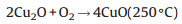
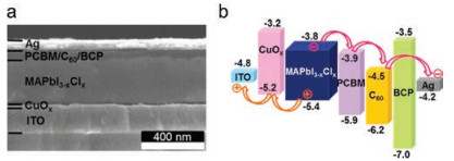
Copper oxide (CuO) and cuprous oxide (Cu2O) are other alternative p-type inorganic semiconductors selected as HTMs in the field of PSC. In theory, due to the narrow band gap of CuO and Cu2O which are 1.4 eV and 2.1 eV, respectively (Fig. 3), these two materials are not regarded as the optimal HTMs. Nevertheless, the merits of high hole mobility (0.129 cm2 V-1 s-1 for CuO and 100 cm2 V-1 s-1 for Cu2O [50]), and low-lying valence band energy levels that match well with perovskite can contribute to the enhancement of HTL. Ding and co-workers [40] designed a simple and novel chemical reaction method, shown in Eqs. (1) and (2), to prepare CuO and Cu2O layers used as HTMs in PSC. The devices yielded a relatively high PCE of 12.16% and 13.35%. The Cu2O film can be achieved by reacting CuI film and aqueous NaOH solution in situ at room temperature. After heating Cu2O film in air, the CuO film is obtained. In this report, the photovoltaic characteristics revealed that CuO-based and Cu2O based cells have higher Voc, Jsc and PCE compared to those based on PEDOT:PSS. Meanwhile, Cu2O PSCs showed better long-term stability. The average PCE for Cu2O cells just decreased by around 1%, from 11.02% to 9.96% after stored for 70 days. By contrast, the performance of the device dramatically declined from 10.11% to 6.79% for PEDOT:PSS sample. In 2016, an excellent efficiency of 19.0% was reported by Rao et al. [41] using CuOx in an inverted planar structure of PSC composed of ITO/CuOx/CH3NH3PbI3/PCBM/C60/BCP/Al (Fig. 6). The CuOx film was deposited by spin-coating Cu(acac)2/1, 2-dichlorobenzene precursor solution. They also adopted a novel Cl doping process to improve the morphology of perovskite layer. The increment of hole mobility, reduction of inherent defects and charge recombination lead to the enhancement of the device performance.

|
Download:
|
| Fig. 6. (a) Cross-sectional SEM image of the ITO/CuOx/MAPbI3-xClx/PCBM/C60/BCP/ Ag device. (b) Schematic illustration of the corresponding energy level diagram. Reprinted with permission [41]. Copyright 2016, Elsevier Ltd. | |

|
(1) |
|
(2) |
Except those three types of inorganic material above, other ptype inorganic semiconductors such as V2O5, CuS, MoO2 have also been explored as HTM to improve the stability and decrease the cost of PSCs. Recently, Ming et al. [42] applied vanadium oxide (V2O5) with free dopants as HTM in the structure of FTO/TiO2/ FA0.85MA0.15PbI2.55Br0.45/V2O5/Au, obtaining a PCE of 11.3%. Furthermore, they fabricated organic-inorganic integrated HTLs involving a nickel (Ⅱ) phthalocyanine (NiPc-(OBu)8) layer and a V2O5 layer. The device based on this integrated layer shows an impressive PCE which is up to 17.6% and better stability than the one with doped spiro-OMeTAD under ambient conditions without encapsulation. After 30 days, the NiPc(OBu)8/V2O5-based cells still retained more than 75% of their initial efficiency. In contrast, the films had already been damaged for the devices containing spiroOMeTAD.
Copper sulphide (CuS) is also a good HTM candidate for PSCs. Rao et al. [43] firstly attempted to utilize CuS nanoparticles (CuS NPs) in an inverted planar heterojunction PSC and successfully modified its surface work function to match with the valence band of perovskite. The introduction of CuS NPs has no effect on the surface roughness and transmittance of ITO substrates but has the ability to promote hole extraction and transportation between the interface of ITO and perovskite layer. Hence, a champion PCE of 16.2% in CuS NPs-based device was achieved.
Molybdenum oxide (MoOx) is considered as one of potential inorganic HTMs in virtue of its non-toxic and air stable nature. For the reason that oxygen vacancies cause various form of Mo cations, Molybdenum oxide is usually a multivalent complex compound consisting of Mo6+, Mo5+ and Mo4+ oxidation states [51]. Kyungmin and co-workers [44] took advantage of scalable solvothermal cracking of polycrystalline MoO3 microparticles technique to synthesize Ti-doped MoO2 nanoparticle based HTM. According to the XPS analysis, they found that both pristine MoO2 and Ti-doped MoO2 represent complicated Mo 3d states with Mo5+ and Mo4+. Eventually, the similar results that a PCE of 15.8% for Ti-doped MoO2 device and 15.7% for pristine MoO2 one were yielded. Moreover, PSCs with Ti-doped MoO2 HTM showed more enhancement in stability against humidity, which is ascribed to stronger Mo-O bonding brought from Ti doping in MoO2.
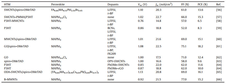
4. Carbon materials based hole transport layer of perovskite solar cellsPerovskite layer is sensitive to humidity, temperature and even long-term light soaking. They are easily degraded by these environmental factors. Carbon materials are thought to be the most promising materials to improve the stability property of PSCs and facilitate their commercialization process. Carbon is cheap, steady, inert to ion migration from perovskite and metal electrodes as well as inherently waterproof [52, 53]. Until now, a great deal of carbon materials have been investigated in PSCs. For instance, fullerene (C60) and its derivatives such as [6, 6]-phenyl C61-butyric acid methyl ester (PCBM) have been used as electron transport layers for PSCs, especially in the inverted planar structure [37, 41]. The electric character and structural order of fullerene materials play an essential role on devices' performance. It has been also proved that fullerene-based materials have the function to suppress hysteresis of PSC, which could impair stability and photovoltaic property of the cells [54]. On the other hand, some carbon materials have been chosen as charge-collecting electrode to replace traditional metal back contacts [55]. The assembled devices are mainly carbon-based hole-conductor-free PSCs and exhibit superior long-term stability. However, in this section, we focus on the progress of utilization of different carbon materials as additives in hole transport layer for PSCs. The list of photovoltaic performance parameters of corresponding devices using different type of carbon based materials is in Table 2.
|
|
Table 2 Photovoltaic properties of perovskite solar cells with the incorporation of various hole transport materials and carbon materials. |
4.1. Single-walled carbon nanotubes
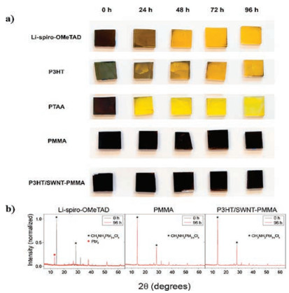
Single-walled carbon nanotubes (SWCNTs) equipped with high conductivity, excellent chemical stability and unique nanostructure have been successfully incorporated into spiro-OMeTAD layer by Aitola et al. [56] They adopted a simple press transfer method to complete the fabrication process of SWCNTs film onto perovskite layer. After densification by chlorobenzene, the SWCNTs was covered by spiro-OMeTAD to form a hybrid hole-transporting layer. The photovoltaic characteristic test demonstrated a relatively reasonable result with a PCE of 13.6% for SWCNTs-spiro-OMeTADbased cell. Even though this value is lower than that of SpiroOMeTAD sample which reached an efficiency of 17.7%, it does provide a new way towards industrialization of PSCs. Habisreutinger et al. [57] compared the decomposition of most commonly used organic HTMs, such as Li-doped spiro-OMeTAD, P3HT and PTAA, with the HTM containing CNTs by exposing the films to the temperature of 80 ℃ for 96 h in ambient air. During the stability test, the P3HT/SWNTs-PMMA coated samples showed no clear changes in color, whereas others with organic HTMs turned yellow completely (Fig. 7) because of the transformation from perovskite to PbI2 as confirmed by XRD. Moreover, with this P3HT/SWCNTPMMA composite structure, a maximum PCE of 15.3% and an average efficiency of (10.4±2.6)% were also achieved in the devices.

|
Download:
|
| Fig. 7. Illustration of the protective effect of various materials on top of perovskite films under thermal stressing. (a) Photo illustrating the visible degradation of the perovskite layer. The color shifts from almost black to yellow for all organic HTLs except for the films covered with PMMA only or a composite of carbon nanotubes and PMMA. (b) X-ray diffraction pattern of devices before (black line) and after (red line) 96 h heat exposure. The spectral changes from the diffraction features characteristic for the CH3NH3PbI3-xClx at 14.28° and 28.57° (black star) to a new diffraction feature at 12.80° associated with PbI2 indicate degradation of the perovskite crystal structure. For the neat PMMA layer and the PMMA-nanotube composite HTL, there are no discernible changes in the diffraction patterns. Reprinted with permission [57]. Copyright 2014, American Chemical Society. | |
4.2. Multi-walled carbon nanotubes
In 2013 [58], the perovskite solar cells based on the incorporation of multi-walled carbon nanotubes (MWCNTs) into P3HT as hole transport materials exhibited an increased efficiency from 4.12% to 6.45%, which is attributed to the great enhancement of fill factor. Since there is π–π interaction between P3HT and MWCNTs and strong electronegative sulphur atoms in P3HT, P3HT would be tightly absorbed on the sidewalls of MWCNTs. Accordingly, MWCNTs play essential roles as charge transport tunnels to induce crystallization of P3HT and promote charge mobility of HTMs. Similarly, our previous work [59] on a new HTM composite based on P3HT and bamboo-structure carbon nanotubes (BCNs) has also demonstrated that a superior morphology of P3HT with compact large grains can be achieved by incorporating BCNs. Raman spectrum results suggested that the BCNs are composed of both SWCNTs and MWCNTs. With addition of 1 wt% BCNs, the crystallinity of P3HT was greatly enhanced, leading to more than one order of magnitude higher conductivity for BCNs-P3HT based HTL and roughly ten-fold reduced charge recombination for th whole device. As a result, a PCE with a value of 8.3% was produced, which is 2-fold higher in comparison with pristine P3HT-based cell. Furthermore, Lee and co-workers [60] embedded MWCNTs in spiro-OMeTAD to enhance carrier concentration, mobility and conductivity. The work function of MWCNTs (-4.6 eV) is higher than the valence band level (-5.4 eV) of perovskite resulting in efficient hole extraction. On the other hand, it is also lower than the conduction band level (-3.9 eV) of perovskite which can create undesirable back-electron transfer. That means the direct electrical contact between perovskite and MWCNTs will increase series resistance and decrease Jsc and Voc thereby limiting the enhancement of PSCs performance. Therefore, a hierarchical structure (Fig. 8) of pure spiro-OMeTAD and spiro-OMeTAD/MWCNTs was developed to block back-electron transfer and take full advantage of the heightened charge transport properties of spiro-OMeTAD/ MWCNTs. An excellent PCE of 15.1% was obtained by using this hierarchical hole transport layer structure.

|
Download:
|
| Fig. 8. Comparison of uniform and hierarchical hole transport layers. a) Schematic of interface between CH3NH3PbI3 and uniform spiro-OMeTAD/MWNT layer. b) Energy band diagram of direct electrical junction between CH3NH3PbI3 and MWNTs. c) Schematic of the interface between CH3NH3PbI3 and hierarchical hole transport layer (pure spiro-OMeTAD/MWNT double layer). d) Energy band diagram of hierarchical electrical junction (CH3NH3PbI3: pure spiro-OMeTAD: MWNT). Reprinted with permission [60]. Copyright 2015, John Wiley and Sons. | |
4.3. Graphene oxide
Graphene, an atom-thick, two-dimensional (2D) and sp2 hybridized carbon material, has been attractive in photovoltaic field, thanks to its exceptional characteristics [67], such as high values of charge-carrier mobility (2 × 105 cm2 V-1 s-1), thermal conductivity (5000Wm-1 K-1), optical transmittance (97.7%) as well as electronic conductivity. As graphene is a zero band gap semiconductor, it always acts as electron transport layer or back contact to extract and collect electron in PSCs [54]. However, graphene oxide (GO) with the applicable work function of -4.9 eV has been employed in HTL for solar cells. Agresti [61] and his group designed a novel mesoscopic perovskite device structure which contains graphene flakes embedded into the mesoporous TiO2 (mTiO2 + G) layer and a graphene oxide layer inserted as interlayer in the interface between perovskite and spiro-OMeTAD film. The combined structure with FTO/compact TiO2 (cTiO2)/mTiO2 + G/ perovskite/GO/spiro-OMeTAD/Au yielded an impressive PCE up to 18.2%. Furthermore, as shown in Fig. 9, the stability tests demonstrated that PSCs with mTiO2 + G possess the best longterm stability under prolonged (16 h) 1 sun irradiation at the maximum power point. In contrast, the perovskite/GO/spiroOMeTAD interface seems to suffer a degradation problem under the same conditions which is possibly a consequence of partial reduction of GO flakes upon irradiation. In inverted planar heterojunction PSCs, graphene oxide was applied directly as hole conductor, MAPbI3-xClx served as light absorber and an optimum PCE over 12% was yielded by Wu and co-workers [62]. It was demonstrated in the report that the introduced GO layer is beneficial to perovskite crystallization and morphology allowing perovskite to form larger textured domains, leading to an almost fully covered film. Even if GO has great potential to enhance charge carrier mobility and retard charge recombination, there is still a big challenge to improve transmittance and reduce sheet resistance without losing the conductivity in GO-based devices [68].

|
Download:
|
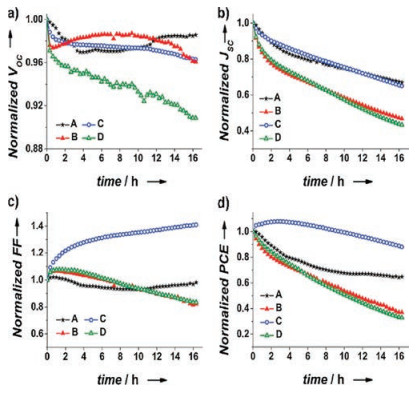
| Fig. 9. Normalized (a) Voc, (b) Jsc, (c) FF, and (d) PCE trends versus time under prolonged 1 sun illumination at MPP polarization provided by a calibrated white LED for devices A–D (A: mTiO2/perovskite/spiro-OMeTAD; B: mTiO2/perovskite/ GO/spiro-OMeTAD; C: mTiO2+G/perovskite/spiro-OMeTAD; ] D: mTiO2+G/perovskite/GO/spiro-OMeTAD). Reprinted with permission [61]. Copyright 2016, John Wiley and Sons. | |
4.4. Functionalized carbon materials
Both n-type and p-type behaviour can be observed in carbon nanotubes and graphene sheets by chemical surface functionalization of carbon. This transformation of semiconductor characteristic between electron donator and electron acceptor is firmly related to the alignment of the Fermi energy level in terms of the frontier orbital energies of carbon materials [69]. The chemical covalent functionalization is different with physically no-covalent functionalization whose modification is through π–π interactions with the surface of carbon materials to complete. Normally, in covalent method, carbon material surface is covalently linked with functional groups via either oxidation or chemical reaction in acidic solutions [70]. The p-type functionalised carbon materials can be applied as independent HTMs or p-type dopants for PSCs to boost carrier mobility and long-term stability of the whole device.
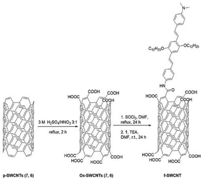
A new covalently functionalized SWCNTs was synthesized by Miletic et al. [63] through amidation reaction of trimeric oligophenylenevinylene (OPV) and oxidized SWCNTs, as shown in Fig. 10. The authors used it as dopants into spiro-OMeTAD to avoid chemical instability of perovskite layer and promote the affinity of SWCNTs with spiro-OMeTAD. The PCE of functionalized SWCNTs-based device was increased to 9.6%, compared to 7.1% of undoped one. Moreover, SWCNTs-doped sample showed better stability. It still has retention of good performance after 45 days of exposure to the environment with 70% humidity and room temperature of (25±1)℃.

|
Download:
|
| Fig. 10. Preparation of OPV-Decorated SWCNTs (7, 6) (f-SWCNT). Reprinted with permission [63]. Copyright 2016, American Chemical Society. | |
In addition, single-walled carbon nanotubes and reduced graphene oxide were decorated with p-methoxyphenyl substituents as organic moieties to create functionalized carbon materials, named PhOMe-SWCNTs and PhOMe-rGO, respectively [64]. This covalently chemical modification of carbon materials guarantees them to have the ability to disperse homogenously and steadily in polymer matrix. After doped into P3HT by small amounts, consequently, the composite HTMs presented enhanced optoelectronic properties compared with pure P3HT. The endurance tests demonstrated that a relatively stable PCE of 11% for PhOMeSWCNTs/P3HT based cell and 7.3% for PhOMe-Rgo/P3HT one were retained over 480 h, which is signified higher than that of undoped P3HT sample.
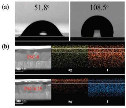
Except the pioneers' reports above, our group [65] reported functionalized carbon materials using octadecylamine. The introduction of ODA-SWCNTs can not only induce perovskite crystal growth into large size, but also improves stability of corresponding devices. In our investigation, because of the hydrophobic nature of ODA-SWCNTs, PSCs showed outstanding resistance to moisture and block migration of iodide reaching metal contact (Fig. 11). After the storage for 45 days under ambient condition with the humidity fluctuated between 60% and 90%, ODA-SWCNTs based cells still achieved 81% of their original PCE. A champion PCE of 16.1% was acquired in the device with triple cation perovskite planar configuration treated by ODA-SWCNTs.

|
Download:
|
| Fig. 11. (a) Characterization of the wettability of as-prepared SWCNT (left) and ODA-SWCNTs (right) measured at 30 s after water droplet deposition. (b) SEM-EDS analysis of PSCs with (PSC-0.25) and without (PSC-0) ODA-SWCNT after aging treatment at an applied bias voltage of 1 V under 1 sun illumination. Reprinted with permission [65]. Copyright 2018, John Wiley and Sons. | |
Boron doped multi-walled carbon nanotubes (B-MWCNTs) were exploited by Zheng and co-workers [66] to improve hole extraction in PSCs, where the assembled device exhibited a PCE exceeding 15% and negligible hysteresis behaviour. The high performance is ascribed to B-MWCNTs which are able to enhance work function, carrier concentration as well as conductivity of MWCNTs. The synthesis of B-MWCNTs can be achieved by the reaction of boric acid and MWCNTs in the quartz tube reactor with pure argon as carrier gas at 1000 ℃ for 4 h. The functionalized MWCNTs were then embedded into perovskite layer and no metal electrodes were required for the cells. Besides, such B-MWCNTs based C-PSCs slowed down the degradation of perovskite film, showing extraordinary long-term stability against high-temperature and high-humidity conditions.
5. Conclusions and outlooksNowadays, although PSCs with organic HTMs have already demonstrated considerably high PCE, the device stability is normally unsatisfactory. It seems inorganic p-type semiconductors such as NiO, CuO and CuO2, CuSCN and some type of carbon materials hold more promise as alternative HTMs for PSCs to overcome that problem. NiO has a broad bandgap, good conductivity, and suitable valence band level that matches with perovskite for effective extraction of photo-generated holes by the perovskite. After doped with Li+ and Mg2+, a PCE of 18.3% for small cell and 16.2% for large cell was obtained. PSCs utilizing CuSCN as HTM yielded PCE exceeding 20% and exhibit high thermal stability under continuing heating. CuO and CuO2 equipped with outstanding hole mobility can give rise to higher Voc and Jsc for devices in comparison with PEDOT:PSS-based cells. On the other hand, carbon materials have a range of beneficial properties involving excellent charge transport characteristics, chemical inertness and mechanical robustness. Thus they are ideal candidates as HTMs or p-type dopants. Carbon nanotubes, both SWCNTs and MWCNTs, have drawn great attention as HTM in PSCs as a result of their unique nanostructure and hydrophobicity, which can overcome moisture vulnerability of perovskite layer and reduce the decomposition of whole device.
Nonetheless, it is significant to note that there are still several aspects regarding the inorganic HTMs and carbon materials that need to be addressed to make stable PSCs with decent efficiency. As for inorganic HTM, (1) the hole mobility of pure inorganic HTMs is not high enough, which will affect the performance of assembled devices. (2) Poor interface contact between the HTM and the perovskite layer will aggravate charge recombination and retard hole transport, leading to low Voc and FF. (3) Most solvents for the deposition of inorganic HTM can partially dissolve and damage the perovskite film. When it comes to carbon materials, the biggest problem is repulsiveness to polar solvent. They have very low solubility either in organic solution or in aqueous solution, which limits the film deposition by solution process. The low-quality surface morphology of carbon material film is another challenge. Pinholes and defects on the surface of carbon layer will expose perovskite causing direct contact with electrode and air, thereby accelerating degradation. Therefore, it is necessary to search solvents which can dissolve or disperse inorganic semiconductors or carbon materials well to fabricate compact, uniform and flat thin film. Functionalizing carbon materials with unique organic groups to impede ion migration inside of cells and decrease hysteresis behaviour is a promising way to enhance the performance of PSCs. Furthermore, we anticipate that the incorporation of proper inorganic p-type semiconductors with functionalized carbon materials as HTM will be a promising research in the future to dramatically reduce the cost and increase long-term stability of PSCs, simultaneously, maintain relatively high power conversion efficiency.
AcknowledgmentsThe authors thank the financial support by Australian Research Council (ARC) through ARC Future Fellowship (No. FT120100674) and Queensland Government through Q-CAS project.
| [1] |
A. Kojima, K. Teshima, Y. Shirai, T. Miyasaka, J. Am. Chem. Soc. 131 (2009) 6050-6051. DOI:10.1021/ja809598r |
| [2] | |
| [3] |
G. Hodes, Science 342 (2013) 317-318. DOI:10.1126/science.1245473 |
| [4] |
H.J. Snaith, A. Abate, J.M. Ball, et al., J. Phys. Chem. Lett. 5 (2014) 1511-1515. DOI:10.1021/jz500113x |
| [5] |
M. Shahbazi, H.X. Wang, Sol. Energy 123 (2016) 74-87. DOI:10.1016/j.solener.2015.11.008 |
| [6] |
C. Wang, J. Yang, Sci. China Mater. 59 (2016) 743-756. DOI:10.1007/s40843-016-5080-1 |
| [7] |
G. Grancini, Roldan-Carmona C., I. Zimmermann, et al., Nat. Commun. 8 (2017) 15684. DOI:10.1038/ncomms15684 |
| [8] |
N.D. Pham, V.T. Tiong, D.S. Yao, et al., Nano Energy 41 (2017) 476-487. DOI:10.1016/j.nanoen.2017.10.006 |
| [9] |
P. Vivo, J.K. Salunke, A. Priimagi, Materials 10 (2017) 1087. DOI:10.3390/ma10091087 |
| [10] |
N. Arora, M.I. Dar, A. Hinderhofer, et al., Science (2017) eaam5655. |
| [11] |
G. Niu, X. Guo, L. Wang, J. Mater. Chem. A 3 (2015) 897-898. |
| [12] |
D. Bi, W. Tress, M.I. Dar, et al., Sci. Adv. 2 (2016) e1501170. DOI:10.1126/sciadv.1501170 |
| [13] |
N.D. Pham, V.T. Tiong, P. Chen, et al., J. Mater. Chem. A 5 (2017) 5195-5203. DOI:10.1039/C6TA11139D |
| [14] |
H. Zhou, Q. Chen, G. Li, et al., Science 345 (2014) 542-546. DOI:10.1126/science.1254050 |
| [15] |
Y. Yang, J. Song, Y.L. Zhao, et al., J. Alloys Compd. 684 (2016) 84-90. DOI:10.1016/j.jallcom.2016.05.154 |
| [16] |
W.S. Yang, B. W. Park, E.H. Jung, et al., Science 356 (2017) 1376-1379. DOI:10.1126/science.aan2301 |
| [17] |
W. Ke, D. Zhao, C.R. Grice, et al., J. Mater. Chem. A 3 (2015) 23888-23894. DOI:10.1039/C5TA07829F |
| [18] |
L. Calió, S. Kazim, M. Grätzel, S. Ahmad, Angew. Chem. Int. Ed. 55 (2016) 14522-14545. DOI:10.1002/anie.201601757 |
| [19] |
W.T.A. Harrison, A.M. Guloy, C.A. Feild, D.B. Mitzi, Nature 369 (1994) 467-469. DOI:10.1038/369467a0 |
| [20] |
H.S. Jung, N.G. Park, Small 11 (2015) 10-25. DOI:10.1002/smll.201402767 |
| [21] |
H. S. Kim, C.R. Lee, J.H. Im, et al., Sci. Rep. 2 (2012) 591. DOI:10.1038/srep00591 |
| [22] |
C. Wang, C. Zhang, S. Wang, et al., Sol. RRL 2 (2018) 1700209. DOI:10.1002/solr.v2.2 |
| [23] |
K. Rakstys, A. Abate, M.I. Dar, et al., J. Am. Chem. Soc. 137 (2015) 16172-16178. DOI:10.1021/jacs.5b11076 |
| [24] |
G. Maculan, A.D. Sheikh, A.L. Abdelhady, et al., J. Phys. Chem. Lett. 6 (2015) 3781-3786. DOI:10.1021/acs.jpclett.5b01666 |
| [25] |
C.C. Stoumpos, C.D. Malliakas, M.G. Kanatzidis, Inorg. Chem. 52 (2013) 9019-9038. DOI:10.1021/ic401215x |
| [26] |
F. Hao, C.C. Stoumpos, R.P.H. Chang, M.G. Kanatzidis, J. Am. Chem. Soc. 136 (2014) 8094-8099. DOI:10.1021/ja5033259 |
| [27] |
M.T. Masood, C. Weinberger, J. Sarfraz, et al., ACS Appl. Mater. Interfaces 9 (2017) 17906-17913. DOI:10.1021/acsami.7b02868 |
| [28] |
M.M. Lee, J. Teuscher, T. Miyasaka, T.N. Murakami, H.J. Snaith, Science 338 (2012) 643-647. DOI:10.1126/science.1228604 |
| [29] |
S. Kazim, M.K. Nazeeruddin, M. Grätzel, S. Ahmad, Angew. Chem. Int. Ed. 53 (2014) 2812-2824. DOI:10.1002/anie.v53.11 |
| [30] |
N. Marinova, S. Valero, J.L. Delgado, J. Colloid Interface Sci. 488 (2017) 373-389. DOI:10.1016/j.jcis.2016.11.021 |
| [31] |
D. Yao, C. Zhang, N.D. Pham, et al., J. Phys. Chem. Lett. 9 (2018) 2113-2120. DOI:10.1021/acs.jpclett.8b00830 |
| [32] |
Z. Yu, L. Sun, Adv. Energy Mater. 5 (2015) 1500213. DOI:10.1002/aenm.201500213 |
| [33] |
P. Qin, Q. He, D. Ouyang, et al., Sci. China Chem. 60 (2017) 472-489. DOI:10.1007/s11426-016-9023-5 |
| [34] |
J.A. Christians, R.C. Fung, P.V. Kamat, J. Am. Chem. Soc. 136 (2013) 758-764. |
| [35] |
A.S. Subbiah, A. Halder, S. Ghosh, J. Phys. Chem. Lett. 5 (2014) 1748-1753. DOI:10.1021/jz500645n |
| [36] |
S. Seo, I.J. Park, M. Kim, Nanoscale 8 (2016) 11403-11412. DOI:10.1039/C6NR01601D |
| [37] |
W. Chen, Y. Wu, Y. Yue, Science 350 (2015) 944-948. DOI:10.1126/science.aad1015 |
| [38] |
W. Chen, Y. Zhou, L. Wang, Adv. Mater. (2018) 1800515. |
| [39] |
N. Wijeyasinghe, A. Regoutz, F. Eisner, et al., Adv. Funct. Mater. 27 (2017) 1701818. DOI:10.1002/adfm.v27.35 |
| [40] |
C. Zuo, L. Ding, Small 11 (2015) 5528-5532. DOI:10.1002/smll.v11.41 |
| [41] |
H. Rao, S. Ye, W. Sun, et al., Nano Energy 27 (2016) 51-57. DOI:10.1016/j.nanoen.2016.06.044 |
| [42] |
M. Cheng, Y. Li, M. Safdari, et al., Adv. Energy Mater. 7 (2017) 1602556. DOI:10.1002/aenm.201602556 |
| [43] |
H. Rao, W. Sun, S. Ye, et al., ACS Appl. Mater. Interfaces 8 (2016) 7800-7805. DOI:10.1021/acsami.5b12776 |
| [44] |
K. Im, J.H. Heo, S.H. Im, J. Kim, Chem. Eng. J. 330 (2017) 698-705. DOI:10.1016/j.cej.2017.07.160 |
| [45] |
M. H. Li, P.S. Shen, K.C. Wang, T.F. Guo, P. Chen, J. Mater. Chem. A 3 (2015) 9011-9019. DOI:10.1039/C4TA06425A |
| [46] |
L. Ai, G. Fang, L. Yuan, et al., Appl. Surf. Sci. 254 (2008) 2401-2405. DOI:10.1016/j.apsusc.2007.09.051 |
| [47] |
Chappaz-Gillot C., S. Berson, R. Salazar, et al., Sol. Energy Mater. Sol. Cells 120 (2014) 163-167. DOI:10.1016/j.solmat.2013.08.038 |
| [48] |
P. Pattanasattayavong, Yaacobi-Gross N., K. Zhao, et al., Adv. Mater. 25 (2013) 1504-1509. DOI:10.1002/adma.v25.10 |
| [49] |
Yaacobi-Gross N., N.D. Treat, P. Pattanasattayavong, et al., Adv. Energy Mater. 5 (2015) 1401529. DOI:10.1002/aenm.201401529 |
| [50] |
R. Rajeswari, M. Mrinalini, S. Prasanthkumar, L. Giribabu, et al., Chem. Rec. 17 (2017) 681-699. DOI:10.1002/tcr.v17.7 |
| [51] |
M.T. Greiner, L. Chai, M.G. Helander, W.M. Tang, Z.H. Lu, Adv. Funct. Mater. 23 (2013) 215-226. DOI:10.1002/adfm.201200993 |
| [52] |
H. Chen, S. Yang, Adv. Mater. (2017) 1603994. |
| [53] |
H. Chen, Z. Wei, K. Yan, et al., Faraday Discuss. 176 (2015) 271-286. |
| [54] |
Z. Wu, T. Song, B. Sun, ChemNanoMat 3 (2017) 75-88. DOI:10.1002/cnma.201600312 |
| [55] |
Z. Liu, M. Zhang, X. Xu, et al., Dalton Trans. 44 (2015) 3967-3973. DOI:10.1039/C4DT02904F |
| [56] |
K. Aitola, K. Sveinbjörnsson, P. Correa-Baena J., et al., Energy Environ. Sci. 9 (2016) 461-466. DOI:10.1039/C5EE03394B |
| [57] |
S.N. Habisreutinger, T. Leijtens, G.E. Eperon, et al., Nano Lett. 14 (2014) 5561-5568. DOI:10.1021/nl501982b |
| [58] |
H. Chen, X. Pan, W. Liu, et al., Chem. Commun. 49 (2013) 7277-7279. DOI:10.1039/c3cc42297f |
| [59] |
M. Cai, V.T. Tiong, T. Hreid, J. Bell, H. Wang, J. Mater. Chem. A 3 (2015) 2784-2793. DOI:10.1039/C4TA04997G |
| [60] |
J. Lee, M.M. Menamparambath, J.Y. Hwang, S. Baik, ChemSusChem 8 (2015) 2358-2362. DOI:10.1002/cssc.v8.14 |
| [61] |
A. Agresti, S. Pescetelli, B. Taheri, et al., ChemSusChem 9 (2016) 2609-2619. DOI:10.1002/cssc.201600942 |
| [62] |
Z. Wu, S. Bai, J. Xiang, et al., Nanoscale 6 (2014) 10505-10510. DOI:10.1039/C4NR03181D |
| [63] |
Miletic' T., E. Pavoni, V. Trifiletti, et al., ACS Appl. Mater. Interfaces 8 (2016) 27966-27973. DOI:10.1021/acsami.6b08398 |
| [64] |
T. Gatti, S. Casaluci, M. Prato, et al., Adv. Funct. Mater. 26 (2016) 7443-7453. DOI:10.1002/adfm.201602803 |
| [65] |
V.T. Tiong, N.D. Pham, T. Wang, et al., Adv. Funct. Mater. 28 (2018) 1705545. DOI:10.1002/adfm.v28.10 |
| [66] |
X.L. Zheng, H.N. Chen, Q. Li, et al., Nano Lett. 17 (2017) 2496-2505. DOI:10.1021/acs.nanolett.7b00200 |
| [67] |
A.C. Ferrari, F. Bonaccorso, Fal'Ko V., et al., Nanoscale 7 (2015) 4598-4810. DOI:10.1039/C4NR01600A |
| [68] |
M. Acik, S.B. Darling, J. Mater. Chem. A 4 (2016) 6185-6235. DOI:10.1039/C5TA09911K |
| [69] |
D.R. Barbero, S.D. Stranks, Adv. Mater. 28 (2016) 9668-9685. DOI:10.1002/adma.201600659 |
| [70] |
P.K. Rai, R.A. Pinnick, Parra-Vasquez A.N.G., et al., J. Am. Chem. Soc. 128 (2006) 591-595. DOI:10.1021/ja055847f |