 2018, Vol. 29


b State Key Laboratory of Urban Water Resource and Environment, Harbin Institute of Technology, Harbin 150001, China
One-dimensional (1D) nanomaterials, such as nanotubes, nanowires (NWs), and nanobelts, have attracted great interest due to their unique physical properties and potential applications in nanoelectronics and nano optoelectronics [1-5]. In the past few decades, many researches have focused on the synthesis and characterization of large quantities of 1D nanostructure. Up to now, nanomaterials with different elements and compounds, such as SiOx [6-8], CdSe [9], MnO2 [10], In2O3 [11] and Si [12-15], have been successfully synthesized by a variety of methods. Of all nanomaterials, silica nanowires have attracted continual attention because of their excellent properties and their broad application prospects, particularly their blue light photoluminescence and optical application [16-19]. Since Wagner et al. first synthesized silica NWs in 1964 with the vapor liquid solid (VLS) growth technique [20], several synthesis methods have been used to synthesize silica NWs including laser ablation [21], chemical vapor deposition (CVD) [22] and solid-state reaction [23] in the existence of different catalysts. However, there are metal contaminations in most synthesis methods. For example, the catalyst keeps on the tip of the nanowires to guide nanowire growth in the VLS mechanism [24]. Therefore, it is crucial to find a method to synthesize aligned and long silica nanowire arrays without metal contamination. Moreover, synthesizing aligned and long silica nanowire arrays without metal catalyst contamination can further broaden the applications as nanoelectrics and as nanointerconnects in integrated optical device.
Recent years, because of the needs of next generation electronics, flexible devices and sensors have attracted enormous attention [25-28]. Capacitors as one of the basic electronic components, have an extensive application in electronics. In order to satisfy the needs of next-generation electronics, flexible or bendable capacitors with high specific capacitance are desired. A parallel-plate capacitor consisting of two parallel conductive plates separated by a dielectric, is the simplest and most frequently used capacitor model [25]. Silicon dioxide with a moderate permittivity of ~3.9 is the conventional insulator used in integrated circuits. But due to its brittle properties, it is incapable of meeting the requirements for flexible devices. For the sake of future flexible applications, it is necessary to replace the insulator with a flexible or bendable dielectric [25]. Silica nanowires have wide band gap, large resistivity, and excellent elastic properties [29, 30], which makes it a good candidate as a bendable dielectric in capacitors.
In this paper, we described a growth method of aligned and long silica nanowire arrays, in which boron was used as catalyst. This method does not need any silicon-based vapor or metal catalyst. The nanowire arrays synthesized by this method possess high yield, high purity (no catalyst contamination) and as long as a few hundreds of micrometers in length. In addition, a large number of silica mircoflowers were achieved by annealing Si and SiO2 powders with boron as catalyst in a quartz tube furnace. And the possible growth models of nanowire arrays and microflowers are proposed. Besides that parallel plate capacitors using the silica nanowire mat as a dielectric were fabricated. The frequency response and mechanical properties of these capacitors were also be investigated and discussed in detail.
The synthesis of SiO2 nanowires arrays was achieved in a hightemperature tube furnace using the milled boron (B) as the catalyst. The schematic diagram of the as-used experimental setup is shown in Scheme S1 (Supporting information). Clean ptype < 100 > silicon wafers, coated with SiO2 layers with thickness of 400 nm by thermal oxidation, were ultrasonically cleaned in toluene, acetone and alcohol in turn and were used as substrates. In order to enhance the catalytic activity of B, crystalline B powder (99%) was first milled for 6 h at a rotating speed of 200 rpm in a horizontal-type high energy ball mill under N2 atmosphere. Then the B powder was dispersed into ethanol solution to form B ink after 15 min ultrosonication. The substrates were local controllable coated with B ink to form catalytic films. The substrates were then placed on the top of an alumina sintering boat in which B, Si and SiO2 powders filled the inside of the boat. The alumina boat was inserted into a tube furnace with the catalytic films facing upward. The substrates were then annealed at 1100 ℃ for 1 h under N2 with 15% H2, and cooled down to room temperature naturally. After growth, white products with stripe patterns were observed on the top side of Si wafer. And snow-white fluffy products were found in the alumina sintering boat.
SiO2 nanowire mats were prepared by compacting SiO2 nanowires with applied pressure. The thickness of the resulting mat could be controlled by varying the mass of SiO2 nanowires used and fixing the area occupied by the nanowires. To prepare a capacitor, the SiO2 nanowire mat was transferred to a polyethylene terephthalate (PET) film (~170μm thick) with conductive silver paste stripe electrodes (2.5–4.0 mm wide, and 2.5 mm long). Then a top silver paste (40 nm thick, 200 μm wide, and 18 mm long) electrode was deposited on the mat.
The morphology and composition analysis of as-grown products were characterized by scanning electron microscophy (SEM, Tescan VEGA 3 SBH) equipped with energy dispersive X-ray spectroscope (EDS, Thermo Scientific), X-ray diffraction (XRD, X'Pert Pro MPD), and transmission electron microscopy (TEM, JEM 2100F at an accelerating voltage of 200 kV). FTIR spectra of the specimens dispersed in KBr disks were recorded on a TENSOR 27 spectrophotometer. The X-ray photoelectron spectroscopy (XPS) was performed on a ThermoFisher ESCALAB 250Xi spectrometer. Current-voltage (I-V) curves were measured using a HP semiconductor characterization system (HP4145B). The capacitance was measured by an impedance analyzer (Fluke PM6306).
Fig. 1 shows the SEM images of the as-grown products on the silicon substrate. It can be observed that high-density aligned silica NWs are synthesized on the silicon substrate. No apparent impurity particles are observed in the SEM images. These vertically aligned nanowires with lengths of a few hundreds of micrometers possess a radial direction on the substrates. Moreover, the aligned nanowires have a uniform diameter (about 550–700 nm) and a columnar structure as shown in Fig. S1a (Supporting information). It can be also observed that most of nanowires have straight configuration, but there are some nanowires with curly configuration. Different with the silica NWs grown on the silicon substrates, large quantities of silica micro-flowers were observed in the alumina sintering boat, as shown in Fig. 1b (Supporting information) and Fig. S1a. The micro-flowers present sunflower-like morphology, in which several tens of silica NWs radially grow upward from disc florets and mutually separate to assemble the petals, forming an obvious 3D flower feature. The diameter of disc florets with planar structures ranges from several hundred nanometers to about 2 μm. The silica NWs consisting of the branches of flowers, have length of 1–4 μm.

|
Download:
|
| Fig. 1. SEM and EDS images of silica nanowires and micro-flowers. | |
The corresponding composition analysis of silica NWs is further investigated by EDS as shown in Fig. 1c. Only strong peaks of Si and O can be observed in the EDS spectrum, indicating that the elements constituting nanowires are Si and O. The atomic ratio of Si to O (1:1.8) is close to 1:2, implying the nanowires are composed of silicon oxide (SiO2). No other elements' peaks are observed in the EDS spectrum, demonstrating that as-synthesized nanowires possess high purity. The EDS spectrum of disc florets of microflowers (Fig. S1c in Supporting information) shows that they consist of B, Si and O, in which B is the primary element and its atomic ratio is 76.25%, indicating that it is the cradle of silica nanowires catalyst-induced. A small amount of Si and O detected in the disc florets indicating that they are composed of a Si–B compound where Si nuclei are oxidized and precipitate to the surface of droplets during the beginning stage of silica formation. We proposed that a silica crown is formed on the surface of the catalyst droplet after the coalescence of SiOx particles. The crown acts as the nucleation and growth site for further growth of SiOx nanowires.
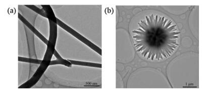
Fig. 2a shows the TEM images of silica nanowires. It can be seen that the diameter of nanowires is uniform and about 200 nm. The most of surfaces of nanowires are considerably clean and smooth. The catalyst particles are not traced in the nanowires, in agreement with the EDS spectrum. In addition, some silica nanowires have branched morphology. The TEM images of silica micro-flowers are shown in Fig. 2b. The TEM study further confirms sunflower-like branched nanostructures consisting of radially attached nanowires (Fig. 2b). And the branches are made up of fine nanowires. The diameters of the nanowires gradually reduce from the root to the tip of nanowire petals (Fig. S2 in Supporting information).

|
Download:
|
| Fig. 2. TEM images of silica nanowires and micro-flowers. | |
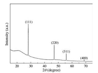
Further composition characterization of the as-grown NWs was performed by XRD pattern, as shown in Fig. 3. It can be observed that four major peaks are observed, in which (111) and (400) peaks are the peaks of cubic structured SiO (JCPDS-04-002-8291), and the broad peak centered between 15° and 25° is attributed to amorphous silica. The peaks corresponding to 2θ values of about 47.3° and 56.1°, are in good agreement with those of the (220) and (311) Si planes, indicating the existence of Si in the as-synthesis silica nanowires. Taken together, the as-synthesized products on the Si wafer are aligned amorphous silica NWs. From the XRD pattern, it should also be noted that no catalyst could be found in the as-synthesis silica nanowires.

|
Download:
|
| Fig. 3. The XRD pattern of as-grown silica nanowires. | |
So far, researchers have posed several growth models about the nanowires or nanotubes, such as vapor-liquid-solid (VLS) growth mechanism, solid-liquid-solid (SLS) growth mechanism, and oxide assisted growth (OAG) growth mechanism. For the VLS mechanism, the main characteristic is the presence of catalyst particles on the top of the nanowires [31]. While, the catalyst particles are more likely to attach to the end of the nanowires in the SLS mechanism [32]. In present work, no catalyst particles can be observed on the tip of the as-grown nanowires, so the VLS mechanism is not appropriate for the SiOx nanowire arrays. For the synthesis of SiOx nanowire arrays in this work, we propose that the following growth mechanism should explain the growth of nanowire arrays.
First, at high temperature, different thermal expansion coefficients result in a tensile stress on SiO2 layer and a compressive stress on Si substrate. Different stresses between them finally induce the crack of SiO2 layer to partially release the stress [33-36], resulting in a stress gradient. Then Si atom could diffuse from Si substrate. Then at high temperature and in N2/H2 atmospheres, the decomposition of SiO2 is suggested to induce the nucleation of SiOx nanowires by following the reaction (1) [31].

|
(1) |
The initial-formed SiOx molecules deposit on the surface of substrate and result in the nucleation of nanowires. While the post-formed SiOx molecules continually stack on the nuclei, leading to the growth of SiOx nanowires.
Furthermore, if the synthesis was carried out under the presented conditions, but without boron addition, no white products were observed, which indicates that boron should act a part in the growth process. We suggest that boron and SiO2 are subjected to a redox reaction to further facilitate the growth of SiOx nanowires. The effect of boron is somewhat similar to the effect of C in the growth process [33]. At high temperature, boron will react with part of SiO2 layer by following reactions (2) and (3):
|
(2) |
|
(3) |
Studies have shown that hydrogen plays a role in the growth of SiOx nanowires [37-39]. The role of hydrogen is to enhance the diffusion kinetics of the silicon atoms. Therefore, we introduce the hydrogen gas in the annealing process to increase the number of Si atoms diffusing from the Si substrate, finally booting the growth of SiOx nanowires.
For the vertically aligned nanowires arrays, the high density of SiOx nucleus results in the concurrent and congested growth of SiOx nanowires. Therefore, the growth of nanowires would be limited by overcrowding effect, restraining the nanowires from growing freely, which has been proposed in earlier report [40]. And SiOx nanowires randomly grow and are not perpendicular to the substrate surface at the uncovered margin, as shown in Fig. 1b, which is accordant with the investigation by Hu et al. [40].
The growth mechanism of some SiOx nanoflowers has been proposed in previous reports [41, 42] However, different from previous reports, which need metal as the catalyst, in our system, no metal catalyst is used. The above SEM and TEM results indicate that B can serve as an effective catalyst for the growth of silica microflowers. According to the analyses of the observed above results, a plausible growth model is proposed for the formation of the microflowers in our experiment, as depicted schematically in Fig. 4. In detail, boron nanoparticles possess high chemical activity and high specific surface area after ball-milling. These nanoparticles catalyze the multiple nucleations of hundreds of silica nanowires distributing on the surface of B nanoparticles. Nanoparticles with high chemical activity agglomerate into catalytic clusters, as shown in Fig. 4a. A small amount of Si condense and dissolve in the B nanoparticles covering the surface of catalytic clusters, as shown in Fig. 4b. Because of a ceaseless supply of Si source, the Si nuclei on the surface of catalytic clusters reach supersaturation. Take into account of the existence of SiO2 powder, the Si nuclei on the surface are oxidized to SiOx. With the increasing and coalescence of SiOx nuclei, a SiOx cap is coated on the surface of Si nuclei as shown in Fig. 4c. The SiOx cap is proposed to act as the seed to grow SiOx naowires petals. The newly formed SiOx molecules stack on the SiOx nuclei, forming silica NWs on the B nanoparticles, as shown in Fig. 4d.

|
Download:
|
| Fig. 4. Schematic diagram of proposed growth model for silica microflowers. | |
The silica nanowires have large band gap and high resistivity, which makes it suitable for use as dielectric material in a parallelplate capacitor. In this paper, a bendable parallel-plate capacitor was fabricated by transferring silica nanowire mats to a PET film. It has a sandwich structure on the PET substrate with two Ag electrodes as bottom and top conductive plates, and a nanowire mat as the dielectric in the middle. The model and optical image of a capacitor on a PET film was shown in Fig. S5 (Supporting information). The PET substrate is transparent.
Fig. 5 shows the frequency response of a capacitor with nanowire mat thickness of 100 μm and an effective area of 4 mm2. The capacitance decreases with increasing frequency from 100 Hz to 20 kHz, with values ranging from 9.4 pF to 7.27 pF. However, the capacitance increases with increasing frequency from 20 kHz to 1.0 MHz, with values ranging from 7.27 pF to 9.9 pF. In addition, only a small amount of capacitance change is found over the frequency range from 4 kHz to 100 kHz, which indicates that the capacitance has small frequency-dependence and good reliability at this frequency range.

|
Download:
|
| Fig. 5. Plot of capacitance of nanowire mat versus frequency. | |
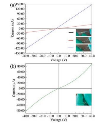
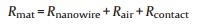
Fig. 6 shows a series of I-V curves of a capacitor under bending, in which the pictures depicted an approximate capacitor bending. The tunneling current increases along with an increase in bending angle of the capacitor. For an initial not-bent capacitor, a meaningful current could be scarcely detected (black curve in Fig. 6a). When the capacitor was slightly bent, a passing current of tens of nA at a voltage of 40 V (red curve in Fig. 6a) was recorded. With increasing in bending angle of the capacitor, the current increase to more than 100 nA at a voltage of 40 V (blue curve in Fig. 6a). Intriguingly, when the capacitor bending angle was nearly equal to 180° (as shown in Fig. 6b), the passing current remarkably increases to tens of μA at a voltage of 40 V. And the I-V curve turns from basically linear to nonlinear. However, during the experiments, when the capacitor was almost retrieved to its initial state, the I-V characteristics were not recovered, as shown in Fig. S6 (Supporting information).

|
Download:
|
| Fig. 6. Serials of the I-V curves along with an increase in bending angle: (a) Fitted I-V curves for the bending angle ≤ 90°; (b) I-V curves for the bending angle approaching 180°. | |
In consideration of above results, we propose an approximate and qualitative model to account for the transport phenomena and resistance decrease under strain. The resistance (Rmat) can be assumed to be composed of three terms (4):
|
(4) |
Where Rnanowire is the resistance of silica NWs. Rair is the resistance of the air in the nanowire mat. Rcontact is the contact resistance which may be composed of the contact resistance of metal-mat junctions, silica NW-silica NW junctions, and nanowire-impurity junctions. The carriers are expected to transmit across the contact barrier through tunneling mode. In the case of parallel-plate capacitor, the total resistance of the capacitor can be described as serial of parallel connections of multiple Rnanowire, Rair and manifold Rcontact, as shown in Fig. S7 (Supporting information).
In this paper, the change of Rair and Rcontact is deemed to play a dominant role on the change of Rmat after bending the capacitor. After bending the capacitor, the nanowire mat was compressed via mechanical deformation, which resulted in a decrease in the amount of air in the mat. Therefore, the Rair decreased during bending the capacitor. On the other hand, the total contact area among nanowire-nanowire increased during bending the capacitor. Besides that, during bending, the tunneling distance among nanowire-nanowire became short. Both of above factors promote the transport of carriers in a region, making for a decrease in Rcontact. In terms of the difference of Rmat of initial state before and after bending, a degree of viscous character of mat should be considered. Due to the viscous character, the amount of air in the mat is smaller than that of mat before bending, leading to a reduction in Rair. Similarly, Rcontact is also smaller than that before bending. Taking above results into consideration, we believe the bendable capacitor based on silica nanowire mat may act as capacitive strain sensors that can be used in electronic fields. More work is needed to further investigate the principle of resistance reduction in the capacitor during bending the capacitor.
In summary, a growth method of aligned and long silica nanowire arrays was developed, in which boron was used to replace metal or carbon as catalyst. The nanowire arrays synthesized by this method possess high yield, high purity (no catalyst contamination) and as long as a few hundreds of micrometers in length with a uniform diameter. In addition, a large number of silica mircoflowers were achieved by annealing Si and SiO2 powders with boron as catalyst in a quartz tube furnance. By comprehensive SEM, TEM and EDS characterizations, we discussed the growth mechanisms of nanowire arrays and microflowers. In view of the fact that silica nanowires have large band gap and high resistivity, bendable capacitors were fabricated by using silica nanowire mat as the dielectric. The frequency response of capacitors was studied. In addition, tunneling current through the capacitor was studied under different bending angles. The tunneling current increases along with an increase in bending angle of the capacitor, which provide a potential application of silica nanowires in the field of nanodevices and strain sensors.
AcknowledgmentsThis work was financially supported by the National Natural Science Foundation of China (No. 61404036), the National Basic Research Program of China (No. 2012CB934104), the Fundamental Research Funds for the Central Universities (Nos. HIT. NSRIF.2015039, 01508536), State Key Laboratory of Urban Water Resource and Environment, Harbin Institute of Technology (No. 2016 TS 06).
Appendix A. Supplementary dataSupplementary data associated with this article can be found, in the online version, at http://dx.doi.org/10.1016/j.cclet.2017.09.039.
| [1] |
J. Hu, T. Odom, C. Lieber, Acc. Chem. Res. 32 (1999) 435-446. DOI:10.1021/ar9700365 |
| [2] |
A. Morales, C. Lieber, Science 279 (1998) 208-211. DOI:10.1126/science.279.5348.208 |
| [3] |
N. Wang, Y. Cai, R.Q. Zhang, Mater. Sci. Eng. R 60 (2008) 1-51. DOI:10.1016/j.mser.2008.01.001 |
| [4] |
A.D. Gamalski, J. Tersoff, R. Sharma, C. Ducati, S. Hofmann, Nano Lett. 10 (2010) 2972-2976. DOI:10.1021/nl101349e |
| [5] |
K. Jun, J.M. Jacobson, Nano Lett. 10 (2010) 2777-2782. DOI:10.1021/nl100662z |
| [6] |
Y.L. Chiew, K.Y. Cheong, Phys. E 42 (2010) 1338-1342. DOI:10.1016/j.physe.2009.11.021 |
| [7] |
Y. Yu, R.Y. Luo, H.D. Shang, Appl. Surf. Sci. 368 (2016) 325-331. DOI:10.1016/j.apsusc.2016.01.251 |
| [8] |
A. Gomez-Martinez, F. Márquez, C. Morant, Appl. Surf. Sci. 387 (2016) 1072-1079. DOI:10.1016/j.apsusc.2016.06.115 |
| [9] |
L.L. Xi, H.B. Ma, G.H. Tao, Chin. Chem. Lett. 27 (2016) 1531-1536. DOI:10.1016/j.cclet.2016.03.002 |
| [10] |
Y.L. Xu, X.Y. Niu, H.L. Chen, S.G. Zhao, X.G. Chen, Chin. Chem. Lett. 28 (2017) 338-344. DOI:10.1016/j.cclet.2016.10.003 |
| [11] |
J.M. Yang, Z.P. Qi, Y.S. Kang, Q. Liu, W.Y. Sun, Chin. Chem. Lett. 27 (2016) 492-496. DOI:10.1016/j.cclet.2015.12.031 |
| [12] |
H. Cui, Y.Y. Lü, G.W. Yang, Y.M. Chen, C.X. Wang, Nano Lett. 15 (2015) 3640-3645. DOI:10.1021/acs.nanolett.5b01442 |
| [13] |
W. Luo, Y.X. Wang, L.J. Wang, et al., ACS Nano 10 (2016) 10524-10532. DOI:10.1021/acsnano.6b06517 |
| [14] |
W. Luo, Y.X. Wang, S.L. Chou, et al., Nano Energy 27 (2016) 255-264. DOI:10.1016/j.nanoen.2016.07.006 |
| [15] |
J.P. Yang, Y.X. Wang, W. Li, et al., Adv. Mater. 29 (2017) 1700523-1700530. DOI:10.1002/adma.v29.48 |
| [16] |
D.P. Yu, Q.L. Hang, Y. Ding, et al., Appl. Phys. Lett. 73 (1998) 3076-3078. DOI:10.1063/1.122677 |
| [17] |
X.C. Wu, W.H. Song, K.Y. Wang, et al., Chem. Phys. Lett. 336 (2001) 53-56. DOI:10.1016/S0009-2614(01)00063-X |
| [18] |
P. Chen, S. Xie, N. Ren, et al., J. Am. Chem. Soc. 128 (2006) 1470-1471. DOI:10.1021/ja057440g |
| [19] |
Y.W. Wang, C.H. Liang, G.W. Meng, X.S. Peng, L.D. Zhang, J. Mater. Chem. 12 (2002) 651-653. DOI:10.1039/b105326b |
| [20] |
R.S. Wagner, W.C. Ellis, Appl. Phys. Lett. 4 (1964) 89-90. DOI:10.1063/1.1753975 |
| [21] |
D.P. Yu, Q.L. Hang, Y. Ding, et al., Appl. Phys. Lett. 73 (1998) 3076-3078. DOI:10.1063/1.122677 |
| [22] |
Z.W. Pan, S. Dai, D.B. Beach, D.H. Lowndes, Nano Lett. 3 (2003) 1279-1284. DOI:10.1021/nl0343203 |
| [23] |
H.K. Park, B. Yang, S.W. Kim, et al., Phys. E 37 (2007) 158-162. DOI:10.1016/j.physe.2006.08.003 |
| [24] |
T.X. Nie, Z.G. Chen, M.T. Niu, et al., J. Phys. Chem. C 117 (2013) 14354-14361. DOI:10.1021/jp403588p |
| [25] |
N. Guo, J.Q. Wei, Y. Jia, et al., Nano Res. 6 (2013) 602-610. DOI:10.1007/s12274-013-0336-4 |
| [26] |
X. Xiao, T.Q. Li, P.H. Yang, et al., ACS Nano 6 (2012) 9200-9206. DOI:10.1021/nn303530k |
| [27] |
D.J. Lipomi, M. Vosgueritchian, B. Tee, et al., Nat. Nanotechnol. 6 (2011) 788-792. DOI:10.1038/nnano.2011.184 |
| [28] |
L.Y. Yuan, X. Xiao, T.P. Ding, et al., Angew. Chem. Int. Ed. 51 (2012) 4934-4938. DOI:10.1002/anie.v51.20 |
| [29] |
L.L.P. Da'vila, V.J. Leppert, E.M. Bringa, Scr. Mater. 60 (2009) 843-846. DOI:10.1016/j.scriptamat.2008.12.057 |
| [30] |
C. Tang, L.L.P. Dávila, J. Appl. Phys. 118 (2015) 094302. DOI:10.1063/1.4929875 |
| [31] |
G.W. Meng, X.S. Peng, Y.W. Wang, et al., Appl. Phys. A 76 (2003) 119-121. DOI:10.1007/s00339-002-1476-7 |
| [32] |
K.H. Lee, H.S. Yang, K.H. Baik, et al., Chem. Phys. Lett. 383 (2004) 380-384. DOI:10.1016/j.cplett.2003.11.056 |
| [33] |
P. Shimpi, P.X. Gao, CrystEngComm 12 (2010) 2817-2820. DOI:10.1039/c000516a |
| [34] |
S.H. Li, X.F. Zhu, Y.P. Zhao, J. Phys. Chem. B 108 (2004) 17032-17041. DOI:10.1021/jp048418x |
| [35] |
S.M. Prokes, S. Arnold, Appl. Phys. Lett. 86 (2005) 193105. DOI:10.1063/1.1925756 |
| [36] |
E.A. de Vasconcelos, F.R.P. dos Santos, E.F. da Silva, H. Boudinov, Appl. Surf. Sci. 252 (2006) 5572-5574. DOI:10.1016/j.apsusc.2005.12.140 |
| [37] |
P. Bratu, U. Hofer, Phys. Rev. Lett. 74 (1995) 1625-1628. DOI:10.1103/PhysRevLett.74.1625 |
| [38] |
H. Kuribayashi, R. Hiruta, R. Shimizu, K. Sudoh, H. Iwasaki, J. Vac. Sci. Technol. A 21 (2003) 1279-1283. DOI:10.1116/1.1586278 |
| [39] |
S.M. Prokesa, S. Arnold, Appl. Phys. Lett. 86 (2005) 193105. DOI:10.1063/1.1925756 |
| [40] |
J.Q. Hu, Y. Jiang, X.M. Meng, C.S. Lee, S.T. Lee, Chem. Phys. Lett. 367 (2003) 339-343. DOI:10.1016/S0009-2614(02)01697-4 |
| [41] |
H. Wang, X.H. Zhang, X.M. Meng, et al., Angew. Chem. Int. Ed. 44 (2005) 6934-6937. DOI:10.1002/(ISSN)1521-3773 |
| [42] |
L.W. Sun, H.P. He, C. Liu, Z.Z. Ye, CrystEngComm 13 (2011) 5807-5812. DOI:10.1039/c1ce05188a |