 2018, Vol. 29


b University of Chinese Academy of Sciences, Beijing 100049, China;
c National & Local Joint Engineering Research Center for Applied Technology of Hybrid Nanomaterials, Collaborative Innovation Center of Nano Functional Materials and Applications of Henan Province, Henan University, Kaifeng 475004, China
The use of renewable energy has attracted more and more attention due to the environmental and energy problems. Solar energy conversion has become a promising process for production of usable forms of energy due to its cleanliness and recyclability [1]. Photocatalytic reaction involves three crucial steps (Fig. 1): (ⅰ) absorption of light to generate electron-hole pairs, (ⅱ) charge separation and transfer (including undesired recombination process through the conduction band (CB) and the valence band (VB) and/or at the defect trapped states in the bulk or on the surface), and (ⅲ) surface reaction (reduction and oxidation reaction of electrons at the CB and holes at the VB, respectively). If the energy of a photon (hv) absorbed exceeds the band gap energy of the semiconductor, an electron will be excited from VB to the CB, leaving a hole behind in the VB. The excited CB electrons and VB holes can recombine and release energy in the form of heat, get trapped in shallow or deep trapped states, or react with electron acceptors and donors adsorbed on the surface of semiconductor. The solar energy conversion efficiency is integrally determined by the each efficiency of the aforementioned three crucial steps. In order to achieve efficient conversion of the solar energy, the following goals aiming to enhance the efficiency of the above three steps are thus claimed: (ⅰ) To harvest as much wide visible light of solar spectrum as possible; (ⅱ) To get efficient separation of electrons and holes by effective strategies; (ⅲ) To promote charge separation and reduce reaction barrier by loading suitable cocatalysts. Meanwhile, the charge separation has been generally considered as one of the most important and challenging factors to affect the photocatalytic performance because the photogenerated electrons and holes are facile to recombine through CB and VB or are trapped by the defect states.

|
Download:
|
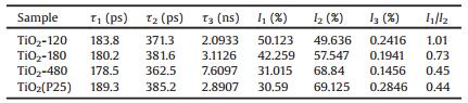
| Fig. 1. Schematic illustration of typical photocatalytic processes. | |
Many researchers have been devoted to theoretically developing models of how recombination affects the solar energy conversion efficiency of photocatalysts and three major models have been proposed up to date. Direct recombination models [2] consider that the electrons and holes recombine before any charge transfer occurs. This type of recombination greatly reduces the efficiency as a result of the fact that little charge has the chance to migrate to surface. The multiple trapping site recombination models [3] describe that the photo-generated charges may recombine at similar trapping sites in single-crystal materials. In this model, a surface-trapped hole can recombine with one of the surface-trapped electrons with similar energy and geometry. The random flight recombination model [4] deals with trapping sites with different energies and can be applied to non-single-crystal systems. This model assumes that electrons transfer between trapped sites via diffusion in the conduction band. That is to say, after an electron is thermally de-trapped from the trapping site into the conduction band, it can subsequently be captured by any empty trapping site or recombine with any holes captured in trapping sites in the lattice or on the surface in the system. If a suitable scavenger is available to trap the electron or hole, recombination is prevented and subsequent redox reactions may occur. Thus, one can deduce that the recombination process is closely related to defect states, which play an important role in charge transfer and migration. In addition, the nature of defects is very complicated [5].
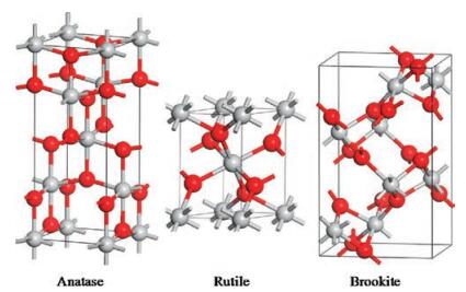
This review will focus on defect engineering in TiO2-based photocatalyst, and provide its basic information such as species, engineering, characterizations for understanding the relationship between defects and photocatalysis for water splitting and environmental purification, and hope to be revealing to designing defect-modulated photocatalysts. TiO2 is a UV-responsive material and one of the earliest studied n-type semiconductor photocatalysts. It ischeap, stable, nontoxic, and environmentallyfriendly and widely used in various fields [6], such as water splitting and environmental purification. Water splitting reaction into H2 is associated with the CB electrons and as for water/air purification, organic pollutants adsorbed are decomposed by the VB holes. TiO2 polymorphs contain anatase, rutile, and brookite and all the three phases are composed of TiO6 octahedra with different arrangements and different surface terminations in various orientations, as shown in Fig. 2. Anatase is generally considered to be the most photocatalyticreactive, rutile is less reactive and brookite is almost nonreactive. Since Fujishima and Honda [7] discovered the phenomenon of photocatalytic water splitting on the TiO2 electrode, scientists have devoted enormous efforts tothe research of this material [8]. The main barriers for the high energy conversion efficiencyof TiO2 arethe poorabsorptionof visible light as well as the rapid recombination of photo-generated charge carriers. As UV light accounts for a very small fraction (5%) of the solar energy compared with visible light (45%), shift in the absorption edge of TiO2 from UV to the visible light region will make a profound positive effect on the practical application of this star material. In addition, because the recombination process is closely related to defect states, it's very important to get insights into the nature of defects as well as their impact on the photocatalytic performance. It should be pointed out that some reports that involve defects and accurate electronic structure analysis on TiO2 but free of photocatalytic performances will not specifically be discussed in this review [9].

|
Download:
|
| Fig. 2. Schematic illustration of the three phases (anatase, rutile, and brookite) of TiO2 (grey sphere represents for Ti atom and red for O atom). | |
2. Main species and basic concepts of defects
Typically, one semiconductor is not a perfect crystal and usually contains different types of defects, which are often divided into three main groups: (ⅰ) point defects (a variety of imperfections involving single atoms), (ⅱ) line defects (linear mismatches in the lattice, such as dislocations or stacking faults) and (ⅲ) plane defects (planar mismatches in the lattice, e.g., grain boundaries, phase boundaries and external surfaces) [10]. Point defects are termed as the defect limited to one structural orlattice site and can be classified as vacancies (a lattice position that is vacant because the atom is missing), interstitials (an atom that occupies a place outside the normal lattice position) and impurities (substitutional or interstitial foreign atoms). In principle, a metal oxide will contain all types of point defects, but a particular type will usually predominate. Vacancies and impurities can also exist as clusters. The typical defects are illustrated in Fig. 3.

|
Download:
|
| Fig. 3. Examples of common defects in semiconductors: (a) interstitial impurity atom, (b) vacancy, (c) self-interstitial atom, (d) substitutional impurity atom (dopant), (e) impurity atoms cluster, (f) vacancy cluster. | |
Titanium dioxide is a non-stoichiometric compound (composition deviates from the chemical formula), which can be represented by the formula TiO2±x, where x is the apparent oxygen nonstoichiometry [9b, 11]. This phenomenon may occur when one ion type can exist in two different valence states (e.g., Ti3+, Ti4+ in TiO2). Valence state of the normal Ti in TiO2 is 4+. If two Ti ions are in 3+ states, then an O vacancy is required to maintain charge neutrality of the compound, leading to the result that less O thanTi atom exists in the compound. TiO2 contains both oxygen and titaniumvacancies and Ti interstitials, which are called as intrinsic defects. Impurityand dopant atoms, which arecalled as extrinsic defects, exist in the form of substituting oxygen or titanium in the lattice sites or filling in the interstitial sites.
Kroeger–Vink notation [12] has been commonly used to describe the formation and reactions of defects. The following species should be taken into consideration for pure TiO2: tetravalent Ti ions in their cation lattice sites (TiTix, neutral); tri-valent Ti ions in the titanium lattice sites (TiTi', equivalent to a quasi-free electron), tetra-valent Ti vacancies (VTi′′′′, equivalent to 4 quasi-free electrons), tetra-valent Ti ions in interstitial sites (Tii····, equivalent to 4 quasi-electron holes), tri-valent Ti ions in interstitial sites (Tii···, equivalent to 3 quasi-electron holes), doubly ionized oxygen ions in the oxygen lattice sites (OOx, neutral), singly ionized oxygen ions in its lattice sites (OO·, equivalent to a quasi-electron hole), doubly ionized oxygen vacancies (VO′′, equivalent to 2 quasi-electron holes). The full chemical formula for undoped TiO2 can be expressed as (TiTix)a (TiTi′)b (VTi′′′′)c (Tii····)d (Tii···)e (OOx)f (OO·)g(VO··)h considering all the defect species mentioned above, and the indices a, b, c, d, e, f, g and h correspond to the molar ratio of the amount of related species. The following conditions must be satisfied: (1) conservation of the lattice site ratio (The sum of molar ratio of all Ti and O lattice species in TiO2 are equal to unity and 2, respectively) and (2) charge neutrality. The lattice is always required to be electrically neutral. The following defect equilibrium equations illustrate formation of the intrinsic defects in TiO2:

|
If a cation vacancy and the cation interstitial or an anion vacancy and the anion interstitial appear in a pair, it is called as Frenkel defects, e.g., VTi′′′′ and Tii···· pair in TiO2. However, additional attention should be paid to the fact that the larger anion atom is not so easy to form an anion interstitial. Pairs of anion and cation vacancies are termed as Schottky defects, e.g., the pair of a lone VTi′′′′ defect and two VO·· defects in TiO2.
Besides the intrinsic defects in undoped TiO2, there are also extrinsic defects that arise from the incorporation of foreign atoms (donated as F atoms) into the crystal lattice. Generally speaking, in the case of incorporation of an F atom at the normal lattice site (A) of a compound, if the F atom has more valence electrons than that of the replaced A atom (acting as a donor and this type of defect can be labeled as FA'), it will cause an occupied level below the conduction band. Oppositely, the F atom with lower valence state will cause an unoccupied level above the valence band (acting as an acceptor and the defect is marked as FA·).
In addition, there are concepts about bulk [13] and surface defects [14] in semiconductors. Bulk defects are vacancies, interstitials, impurities or mismatches in the bulk and can usually affect charge diffusion and structural and electronic properties of semiconductors. Surface defects originating from sudden termination of periodicity of crystal lattice on the surface usually form discrete energy states in the band gap, work as recombination centers [15] (this phenomenon is also found to be detrimental in overall water splitting reaction for rutile TiO2 [16]) or catalytic active sites [17], which will be discussed in detail in the following section.
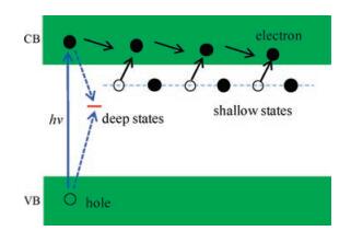
The defects can exist as shallow or deep trapped states. Electrons trapped in the shallow states can easily detrap back to the CB, leading to the fact that this type of defects is beneficial for charge transfer because of the increased carrier densities. However, electrons trapped in the deep level are hard to migrate back to the CB, and will combine with holes, resulting to severe recombination of charge carriers in the recombination centers induced by defect states, as illustrated in Fig. 4.

|
Download:
|
| Fig. 4. Schematic illustration of the transfer and relaxation processes of photogenerated charge carriers concerning the shallow and deep trapped states. | |
3. Typical defect-engineering in TiO2
In the early stage of TiO2-based photocatalyst, the defect sites are normally considered as recombination centers of photogenerated electrons and holes leading to unfavorable photocatalytic performances. The defect sites are generally formed on the surface of one photocatalyst due to its destroyed crystal growth period. Subsequently, the defect sites were found to be formed accompanying with metal/non-metal ion doping due to their unidentical charge. In this case, the metal ion doping can enhance the transfer rate of carriers and/or extend its visible light response, but it also acts as recombination center of carriers. Accordingly, a certain amount of doping is favorable for photocatalytic activity, while excessive amount of metal ion doping will cause decreased photocatalytic activity, and a volcano-type curve of activity dependence on the metal content was usually demonstrated. Recently, researchers have begun to make a good use of defects to widely extend the absorption of solar spectrum or to make them be new active sites. In the following section, we will give a concise illustration on the basic engineering to cause formation of defects, and meanwhile the function of defects will be introduced.
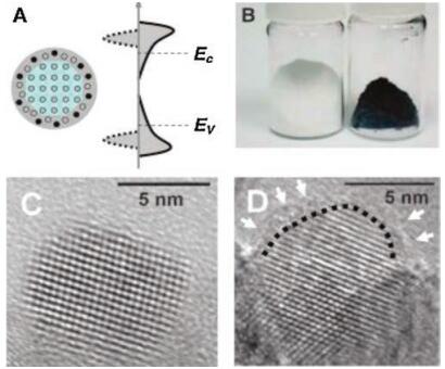
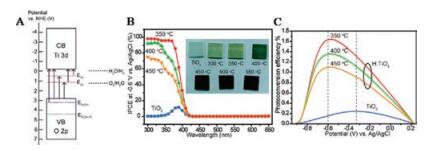
3.1. Hydrogen reductionHydrogenation is a typical method of producing defects to narrow the band gap for extended visible light absorption of TiO2. By heating the sample under H2 stream at elevated temperatures, reduction of TiO2 occurs and defects of oxygen vacancies or Ti interstitials can be obtained. Chen et al. [18] reported that black TiO2 with ~1.0 eV band gap can be achieved by high-pressure hydrogenation treatment, which induces a shift (2.18 eV) of the VB position. They think that the introduced disorder surface layers (Fig. 5) are responsible for efficient infrared photons absorption of TiO2 nanoparticles. However, Wang et al. [19] showed very similar VB spectra for both TiO2 and hydrogenated TiO2 nanowires. They believe that hydrogenation has a negligible effect on the VB position at the TiO2 nanowire surface and the impurity/defect states or oxygen vacancies (VO's) in TiO2 created by hydrogenation play a critical role in extending the visible light absorption. The performance of TiO2 nanowires for photoelectrochemical (PEC) water splitting was remarkably enhanced (Fig. 6). Naldoni et al. [20] found that a broad absorption, starting at about 400 nm and extending into the near-infrared (NIR) region can be obtained after the hydrogenation of the TiO2 nanoparticles, and reason of the band gap narrowing was ascribed to the synergistic presence of VO's and surface disorder.

|
Download:
|
| Fig. 5. (A) Schematic illustration of the structure and electronic DOS of a semiconductor in a disorder-engineered nanocrystal form with dopant incorporation. Dopants are depicted as black dots, and disorder is represented in the outer layer of the nanocrystal. The conduction and valence levels of a bulk semiconductor, EC and EV, respectively, are also shown, and the bands of the nanocrystals are shown at the left. The effect of disorder, which creases broadened tails of states extending into the otherwise forbidden band gap, is shown at the right. (B) An image comparing between unmodified white and disorder-engineered black TiO2 nanocrystals. HRTEM images of TiO2 nanocrystals before (C) and after (D) hydrogenation, respectively. In (D), a short-dashed curve is applied to outline a portion of the interface between the crystalline core and the disordered outer layer (marked by white arrows) of black TiO2. Reprinted with permission [18]. Copyright 2011, AAAS. | |

|
Download:
|
| Fig. 6. (A) A simplified energy diagram of H:TiO2 nanowires. E1o and E2o are referred to the oxygen vacancies (red dashed lines) located at 0.73 eV and 1.18 eV below the TiO2 conduction band; ETi–OH and ETi-OH-Ti (blue dashed lines) located at 0.7 eV and 2.6 eV below the TiO2 valence band represent the energy levels of surface hydroxyl group. The black dashed lines indicate the H2O/H2 and O2/H2O potentials. Arrows highlight the possible electronic transitions between the different energy levels in H:TiO2. (B) IPCE spectra of pristine TiO2 and H:TiO2 nanowires prepared at 350, 400, and 450 ℃, collected at the incident wavelength range from 300 to 650 nm at a potential of -0.6 V vs. Ag/AgCl. Inset: Digital pictures of pristine TiO2 and H:TiO2 nanowires annealed in hydrogen at various temperatures (300, 350, 400, 450, 500, and 550 ℃). (C) Calculated photoconversion efficiencies for the pristine TiO2 and H: TiO2 nanowire samples, as a function of applied potential vs. Ag/AgCl. The dashed lines highlight the optimal potentials for each sample. Reprinted with permission [19]. Copyright 2011, American Chemical Society. | |
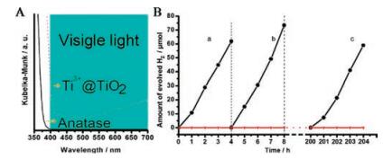
Wang et al. [21] found that a large number of Ti3+ ions and oxygen vacancies can be produced by hydrogenation [22], resulting in improved light absorption and enhanced photocatalytic activity for (001)-facets-dominated anatase TiO2 nanosheets. The higher photoactivities of the reduced self-doped TiO2 nanocrystals have also been attributed to the presence of Ti3+, showing extremely high stability in air and water [23] as illustrated in Fig. 7. A higher concentration of Ti3+ has also been considered to be important in facilitating the charge transfer of electrons or holes [24]. However, the Ti3+ species are not always thought to be beneficial for photocatalytic performances. Wang et al. [25] thought that the localized Ti3+ states were regarded as the recombination centers of photo-generated electrons and holes, which are harmful for the photocatalytic reaction. The reduced concentration of localized Ti3+ states induced by H doping, which is derived from hydrogen treatment, contribute to the inhibited recombination rates of charge carriers leading to improved photocatalytic activity. They noted that the Ti—H bonds in the amorphous shell (TiO2-xHx) could form the intermediate states in the band gap, contributing to extended light absorption. The existence of Ti—H and O—H bonds on the surface of TiO2 was also thought to be responsible for improved visible-light absorption and highly enhanced photocatalytic activity by other workers [21, 26]. Yu et al. found that after hydrogen treatment at elevated temperatures (500–700 ℃), besides the meaningful narrowed band gap, the ratio of surface/bulk defects is also tuned under different hydrogenation condition. Different concentration of oxygen vacancies and Ti3+ interstitials and their varied distribution between surface and bulk can lead to a different photocatalytic performance. A high surface-to-bulk defect ratio (O-/Ti3+) for H-TiO2 prepared at 600 ℃ is considered to be responsible for the enhanced photoactivity. Under that condition, the high concentration of Ti3+ formed in the bulk gradually transform into surface oxygen vacancies as the hydrogenation process goes on [27].

|
Download:
|
| Fig. 7. (A) UV-visible diffuse reflectance spectra for commercial anatase TiO2 (solid line) and sample (dash line). (B) Time course of evolved H2 under visible light (>400 nm) irradiation. (a) reaction for 4 h; (b) evacuate and continue reaction for another 4 h; (c) illuminate for 200 h, evacuate system, and continue reaction for 4 h. (●) Sample; (▼) Anatase. Reprinted with permission [23]. Copyright 2010, American Chemical Society. | |
3.2. Metal doping
Metal doping is another method to introduce defects for band gap narrowing. It implies incorporation of foreign cation atoms into the substitutional or interstitial sites of the parent semiconductor crystal lattice. Doping of cations with lower valence results in increased concentration of holes in the VB and doping of cations with higher valence gives increased concentration of electrons in the CB. The above two types of doping are called p- and n-type dopant, respectively. The bulk electronic structure and surface properties of the parent metal oxide can be altered by the employed cation dopants, which is of lower, equal, and higher valence than that of the substituted parent cation [28].
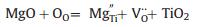
As for metal doping, point defect model has been employed to describe the process. The magnesium-doped TiO2 [29] shows an increased absorption in the visible light region and the process of introducing defects into TiO2 can be expressed in the following equation based on the point defect model,
|
where OO represents normal oxygen ions in the lattice sites; VO·· is oxygen anion vacancy with double positive charge; MgTi′′ indicates Mg atom substitute Ti in the lattice position with two negative charge. The equation shows that Mg doping increases density of oxygen ion vacancies in TiO2 and subsequently promotes the water splitting reaction to H2. Metal ion with small atomic radius, such as Be2+, is considered to be doped in the interstitial site, as demonstrated by Peng et al. [30]. As for the shallow surface doping, the induced oxygen vacancies could work as shallow trapped centers and thus improve the separation efficiency of photogenerated electrons and holes, which is beneficial for charge transfer and the photocatalytic reaction. However, for the deep bulk doping, the trapped electrons cannot migrate to the surface easily and thus led to severe recombination of electrons and holes, decreasing the photocatalytic activities.
Choi et al. [31] had systematically studied the photoreactivity of 21 metal ions doped quantum-sized TiO2 and found that the photoreactivity of doped TiO2 appears to be closely related to the concentration and distribution of dopants, the energy levels of dopants within the TiO2 lattice. The influence of altervalent cation doping of TiO2 on its photocatalytic activity in water cleavage was systematically investigated. It was found that p-type doping of cations with lower valence (In3+, Zn2+, Li+) than that of the parent cation in TiO2 results in decreased rate of water splitting to H2 and enhanced rate of H2 production was obtained by n-type doping with cations of higher valence (W6+, Nb5+, Ta5+) owing to the increased concentration of electrons in the CB. Doping with a cation of an equal valence (Ge4+) does not seem to influence the efficiency for H2 production [28]. But an opposite phenomenon is observed for SrTiO3. Doping of aliovalent metal cations to SrTiO3 was studied carefully to verify doping of a cation with valence lower or higher than that of the parent cation [32]. The defect formation process is illustrated in Fig. 8 based on the point defect model. As seen in Fig. 8A, when a metal cation with lower valence (M3+) is used to substitute Ti4+ in the lattice, half of the oxygen vacancy will be required to maintain the electrical neutrality. In Fig. 8B, doping of a metal cation with higher valence (M5+) is accompanied with the formation of reduced Ti3+ species in the lattice. After checking the photocatalytic water splitting reaction, it was demonstrated that the p-type doping (with lower valence) is more efficient for photocatalytic reaction due to the increased concentration of oxygen vacancies and decreased concentration of Ti3+ ions that are commonly considered to cause deactivation of photocatalyst. On the other hand, n-type doping (with higher valence) results in more Ti3+ species as well as decreased photocatalytic performance. However, Mu et al. [33] found that both n- and p-type doping are harmful to the photoreactivity of TiO2. They thought that the tri- or penta-valent ions will create acceptor or donor levels, which attract charge carriers with the opposite sign, and thereby work as the recombination centers and decrease the photocatalytic efficiency.

|
Download:
|
| Fig. 8. Schematic illustration of aliovalent-doped SrTO3. Doping of (A) trivalent cation and (B) pentavalent cation. Reprinted with permission [32]. Copyright 2009, American Chemical Society. | |
Besides the different ideas of n- and p-type doping, there are also different voices for a certain single metal doping. Transition metal ion doping, such as Cr3+, which substitutes Ti4+ in the lattice matrix with lower valence state, can extend the spectral response of TiO2 to the visible light region by introducing optical transitions from d electrons to the conduction band of TiO2 [34] or Cr3+ to Cr4+ charge transfer [35]. Cr(Ⅲ)-doping was widely reported to promote the photoreactivity of TiO2 in the visible light region. However, different voice argued that the Cr(Ⅲ) doping has an opposite effect on TiO2 and the reason has been attributed to an increase in electron-hole recombination at the Cr3+ ion trapping centers [36]. Doping of other elements, such as Fe [37], V [38], Mo [39], Al [34c, 39], and so on, are also studied and will not be discussed in detail here.
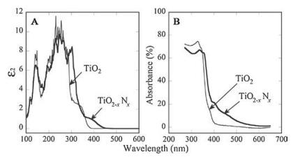
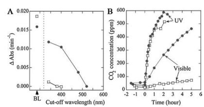
3.3. Nonmetal dopingNonmetal doping is another effective strategy to extend the absorption and enhance the photocatalytic activity. It implies incorporation of a foreign anion atom into the substitutional site in the lattice, because it's hard for an anion with a large atomic radius to occupy the interstitial site. The following requirements should be satisfied: (ⅰ) States in the band gap of TiO2 to efficiently absorb visible light are required to be produced by the doping process; (ⅱ) The impurity states induced by anions should be higher than the H2/H2O level to ensure its photocatalytic activity for the reduction reaction of water splitting; (ⅲ) The states in the forbidden band gap should overlap sufficiently with the band states of TiO2 to transfer photoexcited carriers to reactive sites at the surface of catalyst before recombination process occurs. Various nonmetal (such as N [40], F [41], S [42], B [43], C [44] and P [45]) doped TiO2 nanomaterials have been widely studied for their visible light photocatalytic activities. Of the above nonmetal doped materials, N-doped TiO2 plays an important role in the development of efficient photocatalysts. Asahi et al. [40a] in 2001 firstly reported that nitrogen doped TiO2 can enhance the photocatalytic activity for the photodegradation of methylene blue and gaseous acetaldehyde under visible light irradiation (Figs. 9 and 10). They believe that nitrogen atoms substitute for the lattice oxygen sites and mixture of N2p and O2p is responsible for the visible-light activity. Afterwards, many investigators have reported that doping of nitrogen into TiO2 can effectively tune the band gap to the visible light region and hence improve the performance of photocatalysts [46]. It was also reported that oxygen vacancies induced by N doping contributed to the absorption as well as photoactivity in the visible light region [47]. There are also other voices [48] that oxygen vacancy defects in the bulk induced by doping of N into the lattice of TiO2 can act as recombination centers for charge carriers leading to the decreased photocatalytic efficiency. Therefore, a loss of UV-activity usually appears for N-doped TiO2 compared to pure TiO2, which is due to the rapid recombination of photogenerated electrons and holes caused by deep trapping of the impurity levels.

|
Download:
|
| Fig. 9. Optical properties of TiO2-xNx (thick lines) compared with TiO2 (thin lines). (A) Calculated imaginary parts of the dielectric functions (ε2), which are averaged over three (x, y, and z) polarization vectors. (B) Experimental optical absorption spectra of TiO2-xNx and TiO2 films. Reprinted with permission [40a]. Copyright 2001, AAAS. | |

|
Download:
|
| Fig. 10. Photocatalytic properties of TiO2-xNx samples (solid circles) compared with TiO2 samples (open squares). (A) Decomposition rates [measuring the change in absorption of the reference light (Δabs)] of methylene blue as a function of the cutoff wavelength of the optical high-path filters under fluorescent light with the integrated photon flux of 2.45 ×10⁻⁹ einstein (E) s-1 cm-2 between 350 nm and 520 nm, compared with the results under BL illumination with the integrated photon flux of 3.51 ×10⁻⁹ E s-1 cm-2 in the UV range. (B) CO2 evolution as a function of irradiation time (light on at zero) during the photodegradation of acetaldehyde gas [with an initial concentration of 485 parts per million (ppm)] under UV irradiation (BL with a peak at 351 nm and the light power of 5.4 mW/cm2 and visible irradiation [fluorescent light cut by the optical high-path filter (SC42, Fuji photo film), with a peak intensity at 436 nm and a light power of 0.9 mW/cm2. Reprinted with permission [40a]. Copyright 2001, AAAS. | |
The correlation between defects and doping strategies in TiO2 has been revealed. In addition to the above-mentioned metal or nonmental doping, there are also many investigations about codoped strategies using metal-nonmetal [49] or nonmetal-nonmetal ions [50]. The codoped system is more complicated and apparently be affected by the preparation methods and doping procedures such as doping one element first and then another or simultaneously introducing the two doped elements. Efforts are in progress to improve the photocatalytic performances of TiO2 using co-doped strategies and also disclose the nature behind it. Trapped states in such system are usually associated with the two codoping ions and it's of course more difficult to reveal the role of each of the two doped elements in such systems compared with single element doping systems.
3.4. OthersThe ideal defect-free surface is considered not reactive at room temperature [14b, 51]. Defects, such as Ti centers (for example Ti3+ species [51a]), oxygen and titanium vacancies, play an important role in changing chemical adsorption and which can work as active sites [52]. For example, oxygen vacancy is reported to work as active site to reduce metal in situ to get defect-based composite photocatalyst [53]. Fast reduction of metal ions on the TiO2-OV (oxygen vacancy) without any additional reducing agents or surfactants for deposition of gold ions is introduced as a novel strategy. The direct electron transfer from the oxygen vacancy states of TiO2-OV to the gold ions is thought to be responsible for such a fast and spontaneous formation of metallic gold nanoparticles. Ti vacancy in the surface is considered as active site to adsorb H2O molecule to get activated complex, which is beneficial for water splitting reaction [17a]. It is considered that the presence of surface active sites is essential for the effective charge transfer between TiO2 and water molecule to effectively provide electron holes to the adsorbed water molecules.
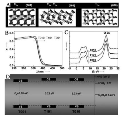
TiO2 with crystal facets in different orientations shows different coordination atoms, such as 4-, 5-, 6-coordinated Ti atom. The 6- coordinated Ti is the normal Ti atom in the lattice matrix, while the 4- and 5-coordinated Ti are under-coordinated and considered as defects in the surface. It is generally considered that a facet with a high percentage of under-coordinated atoms shows much better performance than that with a low percentage of under-coordinated atoms [54]. By tuning the different ratio of facets exposed with different types and percentages of under-coordinated Ti atoms, the photoactivity of TiO2 can be adjusted as a result of the different ability of the adsorption of reactants, surface transfer between photogenerated electrons and the reactant molecules, and desorption of products [55]. As shown in Fig. 11, Pan et al. [54d] showed that the best photocatalytic performance was obtained on T010 in anatase TiO2 by considering both the effects of surface atomic coordination and band structure. On the one hand, the {001} and {010} shows higher photocatalytic activity considering more surface Ti5c atoms compared to {101}. On the other hand, the higher CB minimums of {101} and {010} than {001} are beneficial for the photocatalytic performance due to the stronger reductive driving force. As a whole, the {010} shows the highest reactivity.

|
Download:
|
| Fig. 11. Surface atomic structure and electronic structure. (A) Schematic of atomic structure of {101}, {001}, and {010} faces. (B) UV/vis absorption spectra of T001, T101, and T010. (C) Valence-band XP spectra of T001, T101, and T010. (D) Determined valence-band and conduction-band edges of T001, T101, and T010. Reprinted with permission [54d]. Copyright 2011, WILEY-VCH Verlag GmbH & Co. KGaA, Weinheim. | |
To summary, the defect engineering of TiO2 can be achieved by hydrogenation, metal or nonmetal doping and also calcinations [56], which are the most common and simple methods. Defective sites can work as recombination centers [57] causing decrease of the photocatalytic efficiency, or play a positive role in harvesting extended visible light for utilization of more solar energy, or work as catalytic active sites in certain conditions.
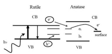
4. Typical characterizations of defectsTo characterize defects, electron paramagnetic resonance (EPR) as a form of magnetic resonance spectroscopy is employed to detect unpaired (or free) electrons and is active for the surface and lattice trapping sites, such as O- (electron hole trapped in oxygen lattice site) and Ti3+ (electron trapped in titanium lattice site) species in TiO2 [4b, 52b, 58]. It is a widely used method to investigate the photocatalytic behavior and charge separation dynamics in TiO2 at the molecular level. For example, Hurum et al.[59] excited anatase, rutile and P25 with visible light (>400nm) and UV light separately at 10K to get EPR signals. In the resultant EPR spectrum, there are two major features: signals from holes and signals from electrons. As shown in Fig. 12, a broad signal at g=2.014 is assigned to surface hole trapping sites (O- species). The sharp signal at g⊥=1.990 and shoulder at g||=1.957 are assigned to lattice electron trapping sites (Ti3+ species) in anatase (see the blue lines) and the remaining signals at g⊥=1.975 and g||=1.940 are the lattice electron trapping sites in rutile (see the green lines). No signal is observed in anatase under the experimental visible light illumination (red curves) and presence of the anatase Ti (Ⅲ) signal in the P25 sample under visible light confirms the charge transfer from rutile to anatase. Their results demonstrated that small rutile crystallites present in P25 facilitate rapid electron transfer from rutile to the lower energy lattice trapping sites of anatase under visible light illumination, leading to an enhanced charge separation process. Electrons trapped in the anatase trapping sites subsequently moves to the surface trapping sites, further facilitating the electron-hole separation. The rutile phase is thought to work as an antenna to extend the absorption region into visible light and catalytic "hot spots" is created at the rutileanatase interface (Fig. 13). Amano et al. [60] investigatedthe effects of high-temperaturecalcination and H2 reductiontreatmenton the water oxidation activity of rutile TiO2 under UV irradiation. Electron spin resonance (ESR) spectra shows that signals of O- species (g=2.061, trapped hole in oxygen lattice site) induced by calcinations disappeared and signals of Ti3+ species (g=1.974, trapped electron in Ti lattice site) and oxygen vacancies (g=2.002, trapped electron in oxygen vacancy) became sharp after H2 treatment at 500 ℃, demonstrating that the high-temperature calcination created O- (acceptor doping) species and H2 reduction treatment created Ti3+ and oxygen vacancies (donor doping). The increased density of electrons in shallow traps and conduction band after H2 treatment is thought to be one of the most important factors for the improvement of the photocatalytic activity of rutile TiO2.

|
Download:
|
| Fig. 12. EPR spectra of a P25 aqueous slurry under visible (marked in red) and UV illumination, in comparison to those of rutile and anatase under UV and visible (marked in black) illumination. Note the absence of any anatase signal under the experimental visible illumination conditions. Reprinted with permission [59]. Copyright 2003, American Chemical Society. | |

|
Download:
|
| Fig. 13. Proposed model of a rutile antenna and subsequent charge separation process in P25. Reprinted with permission [59]. Copyright 2003, American Chemical Society. | |
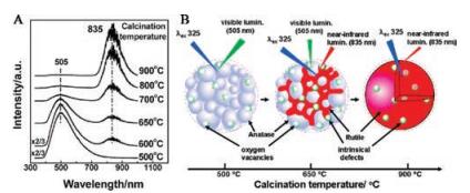
The photogenerated carriers can be trapped and quenched by defect states and electron–hole recombination can take place and release energy in the form of light irradiation. Based on the above principles, photoluminescence spectra or time-resolved photoluminescence spectra (PL or time-resolved PL) have been widely employed to investigate the properties of photocatalysts and give information of the defects. PL is one of the most powerful techniques for investigating the trap states and characterizing the irradiative recombination processes of photogenerated charge carriers [61]. Time-resolved PL can give information about lifetimes and dynamics of photogenerated electrons and holes and distribution of trapped states [61e, 62]. Long-lived charge carriers with slow decay dynamics are thought to be beneficial for the photoactivity. By studying the photoluminescence characteristics of TiO2, Shi et al. [63] studied the relationship between the emission characteristics and photocatalytic performance of TiO2. As illustrated in Fig. 14, they found that the visible luminescence band centered at about 505nm is ascribed to oxygen vacancies in anatase TiO2, while the near-infrared luminescence band centered at 835nm is caused by intrinsic defects in rutile TiO2. Deposition of Pt on the photo-induced electrons in anatase TiO2 surface leads to obvious quenching of the visible luminescence band and less change in the near-infrared luminescence band, demonstrating that electrons trapped in oxygen vacancies of anatase transferred to Pt easily to participate in the photocatalytic reduction reaction and the electrons trapped in the intrinsic defects of rutile still recombine by the way of near-infrared emission. PL is a powerful technique for investigating the trap states and their effects on carrier dynamics, which is very helpful for characterizing semiconductor materials and understanding the photocatalytic process. Similarly, the cathodoluminescence (CL) technique is another similar method to study defects and the recombination process of photogenerated electrons and holes [20, 64]. The principles of CL are similar to that of PL. Instead of photons used in the PL method, electrons with high energy are employed to excite the photocatalysts and thus charge carriers are generated in the CL technique.

|
Download:
|
| Fig. 14. (A) Photoluminescence spectra of TiO2 calcined at different temperatures. (B) Schematic illustration of the photoluminescence evolution with the phase transformation of TiO2 from anatase to rutile at elevated temperatures. Reprinted with permission [63]. Copyright 2007, American Chemical Society. | |
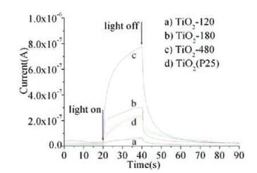
The positron annihilation spectroscopy (PAS) is a sensitive method for determining the vacancy-type defects and their number, which has been proven as a useful tool in investigating the intrinsic defects in semiconductors [65]. Measurements of positron lifetimes can provide valuable information about the defect structure in a solid. When positrons are injected inside the bulk of materials, thermalized positrons move in interstitial sites in the lattice because of strong coulombic repulsion by the lattice ions, annihilate with electrons (positron-electron interaction) and release heat, leading to the emission of γ rays, which can provide information of the lifetime of positrons. Vacancy defects can act as positron traps if they are neutral or negatively charged and positively charged defects are generally not considered to be effective positron traps [57a], as a result of the fact that positive defects are expected to repel positrons and negatively charged defects are expected to be strongly attractive to positrons because of their long-range coulomb potential. The smaller lifetime (τ1) is generally due to the free annihilation of positrons in a defect-free crystal and denoted as the first lifetime of positrons. However, imperfect smaller vacancies (such as mono-vacancies, etc.) will decrease the average electron density and the annihilation rate, leading to a prolonged lifetime of τ1. The second longer lifetime (2) arises from positrons captured by defects of larger size (such as oxygen vacancy clusters) due to the fact that the surrounding electron density in larger-sized defects is lower than that of smallsized defects. A crystal containing positron traps generally gives an experimental lifetime spectrum characterized by an average lifetime, which is related to τ1 and τ2, and the positron trapping rate [66]. In addition, the third longest component (τ3) for all samples was probably due to the annihilation of orthopositronium atoms formed in the large voids present in the material. Kong et al. [27b] synthesized TiO2 nanocrystals with tuned bulk/surface defects and then characterized them by positron annihilation. It's considered that the small-sized defects mainly exist in the bulk of TiO2 and the larger-sized defects mainly locate on the surface or subsurface. Higher photocatalytic activity occurs at the smaller ratio of I1/I2 (I1 and I2 represents relative intensity of the τ1 and τ2 processes, respectively), suggesting that the smaller ratio of bulk/ surface defects concentration is beneficial for the photocatalytic process (Table 1 and Fig. 15).
|
|
Table 1 Positron lifetime and relative intensities of the TiO2 samples. |

|
Download:
|
| Fig. 15. Transient response of the photocurrent for the TiO2 samples under the UV irradiation in air. Reprinted with permission [27b]. Copyright 2011, American Chemical Society. | |
Other methods have been also employed to study the defects. For example, deep level transient spectroscopy (DLTS) [67] is a high-frequency capacitance transient thermal scanning method for observing a wide variety of traps in semiconductors. The basic principle is the concepts of p-n junction capacitance transients due to the filling and emptying of deep level traps (impurity or defect states near CB or VB) at a fixed temperature. The sign of the peak indicates whether the trap is near the conduction or valence band (trapping electrons or holes, respectively) and the height of the peak is proportional to concentrations of the trap states. Other methods, such as X-ray (or ultraviolet) photoelectron spectroscopy (XPS, or UPS), infrared spectroscopy or time-resolved infrared spectroscopy [ 47c, 68] (IR or time-resolved IR), Photoacoustic spectroscopy [69] (PS), scanning tunneling microscopy [70] (STM, which is often used in the surface science), the resonant photoelectron diffraction [69a, 71], low-temperature specific heat [72] (LTSH), low energy electron diffraction [73] (LEED), energyloss spectroscopy [74] (ELS) and so on, are also frequently employed to study defects.
5. Summary and prospectsIn summary, defects have been widely investigated in different research fields, but few reviews have been delivered. In this minireview, point defects are basically interpreted by using TiO2 as the model photocatalyst, but it should be pointed out that the concepts are not limited to the TiO2 itself, and which exist in many other semiconductor materials and different fields such as the surface science, conventional catalysis, luminescent materials, biology, and so on.
There are some ordinary methods for defect engineering, such as hydrogenation treatment, metal or nonmetal doping, calcinations, and so on. The defects can work as active sites to facilitate the catalytic reaction, extend the absorption edge of semiconductors to the visible light region (the defect states here will exist as the donor or acceptor levels in the forbidden band gap near the VB or CB position) to make a better use of the solar spectrum and also increase the charge carrier density as shallow trapped states. However, the deep trapped states will work as recombination centers, causing unfavorable charge transfer process as well as decreased catalytic performance.
A variety of methods can be employed to investigate defects in semiconductors, such as EPR, PL or time-resolved PL, PAS, DLTS, XPS or UPS, IR or time-resolved IR, STM, and so on. Further research and characterization is still required to reveal the nature of defects and establish the foundation of defect engineering.
As a whole, the defects play a complicated and sometimes confusing role in TiO2-based photocatalytic processes, because many factors can affect the performance and different voices always exit. For example, different preparation methods can also have a significant impact on the properties of semiconductors, leading to distinct electronic and structural properties of photocatalysts and existence of varied types of defects. Some of them play a positive effect and others may be negative. The resultant catalytic performance is related to the balance of the advantages and disadvantages of those contrary aspects. Alternatively, defect engineering has received more attention in various fields and is also important for us to promote performances of photocatalysts. More work need to be done to reveal the nature of defects and characterize them as possible to guide us to synthesize catalysts with high performance in the future.
AcknowledgmentsThis work was financially supported by the Basic Research Program of China (973 Program, No. 2014CB239403), the National Natural Science Foundation of China (Nos. 21633009, 21373210, 21522306). F. Zhang thanks the priority support from the "Hundred Talents Program" of Chinese Academy of Sciences.
| [1] |
(a) J. Nowotny, Energy Environ. Sci. 1 (2008) 565-572; (b) H. J. Yu, R. Shi, T. R. Zhang, et al., Adv. Mater. 29 (2017) 1605148; (c) Y. F. Zhao, X. D. Jia, T. R. Zhang, et al., Adv. Energy Mater. 6 (2016) 1501974. |
| [2] |
J. Bisquert, A. Zaban, P. Salvador, J. Phys. Chem. B 106 (2002) 8774-8782. DOI:10.1021/jp026058c |
| [3] |
(a) G. Adriaenssens, S. Baranovskii, Ö. Öktü, et al., Phys. Rev. B 51 (1995) 9661-9667; (b) J. Noolandi, Phys. Rev. B 16 (1977) 4466-4473; (c) F. W. Schmidlin, Phys. Rev. B 16 (1977) 2362-2385. |
| [4] |
(a) A. Barzykin, M. Tachiya, J. Phys. Chem. B 106 (2002) 4356-4363; (b) D. C. Hurum, K. A. Gray, J. Phys. Chem. B 109 (2005) 977-980. |
| [5] |
M.K. Nowotny, L.R. Sheppard, T. Bak, J. Nowotny, J. Phys. Chem. C 112 (2008) 5275-5300. DOI:10.1021/jp077275m |
| [6] |
Y. Ma, X. Wang, C. Li, et al., Chem. Rev. 114 (2014) 9987-10043. DOI:10.1021/cr500008u |
| [7] |
A. Fujishima, Nature 238 (1972) 37-38. DOI:10.1038/238037a0 |
| [8] |
(a) P. Zhang, M. Fujitsuka, T. Majima, J. Energy Chem. 25 (2016) 917-926; (b) W. Zhang, T. Zhou, J. Hong, R. Xu, J. Energy Chem. 25 (2016) 500-506; (c) C. Wu, Z. Gao, Y. Dai, et al., J. Energy Chem. 25 (2016) 726-733. |
| [9] |
(a) M. Batzill, E. H. Morales, U. Diebold, Phys. Rev. Lett. 96 (2006) 026103; (b) M. Nowotny, T. Bak, J. Nowotny, J. Phys. Chem. B 110 (2006) 16270-16282. |
| [10] |
(a) U. Diebold, Surf. Sci. Rep. 48 (2003) 53-229; (b) P. Kofstad, Oxid. Metal. 44 (1995) 3-27. |
| [11] |
T. Bak, J. Nowotny, M. Nowotny, J. Phys. Chem. B 110 (2006) 21560-21567. DOI:10.1021/jp063700k |
| [12] |
F. Kröger, H. Vink, J. Phys. Chem. Solids 5 (1958) 208-223. DOI:10.1016/0022-3697(58)90069-6 |
| [13] |
D. M. Smyth, The Defect Chemistry of Metal Oxides, Oxford University, 2000.
|
| [14] |
P. Wynblatt, R. McCune, J. Nowotny, L. Dufour, Surface and Near-Surface Chemistry of Oxide Materials, Elsevier, Amsterdam, 1988.
|
| [15] |
L.M. Peter, J. Li, R. Peat, J. Electroanal. Chem. 165 (1984) 29-40. DOI:10.1016/S0022-0728(84)80084-4 |
| [16] |
K. Maeda, N. Murakami, T. Ohno, J. Phys. Chem. C 118 (2014) 9093-9100. DOI:10.1021/jp502949q |
| [17] |
(a) J. Nowotny, T. Bak, M. K. Nowotny, L. R. Sheppard, J. Phys. Chem. B 110 (2006) 18492-18495; (b) S. Polarz, J. Strunk, M. Driess, et al., Angew. Chem. Int. Ed. 45 (2006) 2965-2969. |
| [18] |
(a) X. B. Chen, L. Liu, P. Y. Yu, S. S. Mao, Science 331 (2011) 746-750; (b) Y. Liu, L. Tian, X. B. Chen, et al., Sci. Bull. 62 (2017) 431-441. |
| [19] |
G. Wang, H. Wang, Y. Li, et al., Nano Lett. 11 (2011) 3026-3033. DOI:10.1021/nl201766h |
| [20] |
A. Naldoni, M. Allieta, V. Santo, et al., J. Am. Chem. Soc. 134 (2012) 7600-7603. DOI:10.1021/ja3012676 |
| [21] |
W. Wei, N. Yaru, L. Chunhua, X. Zhongzi, RSC Adv. 2 (2012) 8286-8288. DOI:10.1039/c2ra21049e |
| [22] |
H. Liu, H. Ma, X.H. Bao, et al., Chemosphere 50 (2003) 39-46. DOI:10.1016/S0045-6535(02)00486-1 |
| [23] |
F. Zuo, L. Wang, P. Feng, et al., J. Am. Chem. Soc. 132 (2010) 11856-11857. DOI:10.1021/ja103843d |
| [24] |
I. Justicia, P. Ordejón, A. Figueras, et al., Adv. Mater. 14 (2002) 1399-1402. DOI:10.1002/1521-4095(20021002)14:19<1399::AID-ADMA1399>3.0.CO;2-C |
| [25] |
Z. Wang, C. Yang, M. Jiang, et al., Adv. Funct. Mater. 23 (2013) 5444-5450. DOI:10.1002/adfm.v23.43 |
| [26] |
Z. Zheng, B. Huang, H. Whangbo, et al., Chem. Commun. 48 (2012) 5733-5735. DOI:10.1039/c2cc32220j |
| [27] |
(a) X. Yu, B. Kim, Y. K. Kim, ACS Catal. 3 (2013) 2479-2486; (b) M. Kong, Y. Li, X. Zhao, et al., J. Am Chem. Soc. 133 (2011) 16414-16417. |
| [28] |
K.E. Karakitsou, X.E. Verykios, J. Phys. Chem. 97 (1993) 1184-1189. DOI:10.1021/j100108a014 |
| [29] |
J. Kiwi, M. Gratzel, J. Phys. Chem. C 90 (1986) 637-640. DOI:10.1021/j100276a031 |
| [30] |
S. Peng, Y. Li, S. Li, et al., Chem. Phys. 398 (2004) 235-239. |
| [31] |
W. Choi, A. Termin, M.R. Hoffmann, J. Phys. Chem. 98 (1994) 13669-13679. DOI:10.1021/j100102a038 |
| [32] |
T. Takata, K. Domen, J. Phys. Chem. C 113 (2009) 19386-19388. DOI:10.1021/jp908621e |
| [33] |
W. Mu, J.M. Herrmann, P. Pichat, Catal. Lett. 3 (1989) 73-84. DOI:10.1007/BF00765057 |
| [34] |
(a) E. Borgarello, J. Kiwi, M. Visca, et al., J. Am. Chem. Soc. 104 (1982) 2996-3002; (b) A. K. Ghosh, H. P. Maruska, J. Electrochem. Soc. 124 (1977) 1516-1522; (c) H. P. Maruska, A. K. Ghosh, Sol. Energy Mater. 1 (1979) 237-247; (d) J. Zhu, Z. Deng, L. Zhang, et al., Appl. Catal B: Environ. 62 (2006) 329-335; (e) J. Choi, H. Park, M. R. Hoffmann, J. Phys. Chem. C 114 (2010) 783-792. |
| [35] |
A. Mackor, G. Blasse, Chem. Phys. Lett. 77 (1981) 6-8. DOI:10.1016/0009-2614(81)85588-1 |
| [36] |
(a) J. M. Herrmann, J. Disdier, P. Pichat, Chem. Phys. Lett. 108 (1984) 618-622; (b) N. Serpone, D. Lawless, Langmuir 10 (1994) 643-652. |
| [37] |
(a) J. Zhu, F. Chen, J. Zhang, H. Chen, M. Anpo, J. Photochem. Photobiol. A: Chem. 180 (2006) 196-204; (b) S. Klosek, D. Raftery, J. Phys. Chem. B 105 (2001) 2815-2819; (c) X. Wang, J. G. Li, T. Ishigaki, et al., J. Phys Chem. B 110 (2006) 6804-6809; (d) M. Litter, J. A. Navio, J. Photochem, Photobiol. A: Chem. 98 (1996) 171-181. |
| [38] |
J.C.S. Wu, C.H. Chen, J. Photochem. Photobiol. A:Chem. 163 (2004) 509-515. DOI:10.1016/j.jphotochem.2004.02.007 |
| [39] |
Z. Luo, Q.H. Gao, J. Photochem. Photobiol. A:Chem. 63 (1992) 367-375. DOI:10.1016/1010-6030(92)85202-6 |
| [40] |
(a) R. Asahi, T. Morikawa, T. Ohwaki, K. Aoki, Y. Taga, Science 293 (2001) 269-271; (b) J. L. Gole, J. D. Stout, C. Burda, Y. Lou, X. Chen, J. Phys. Chem. B 108 (2004) 1230-1240; (c) P. G. Wu, C. H. Ma, J. K. Shang, Appl. Phys. A 81 (2005) 1411-1417. |
| [41] |
(a) J. C. Yu, J. Yu, L. Zhang, et al., Chem. Mater. 14 (2002) 3808-3816; (b) J. G. Yu, C. Y. Jimmy, K. Iu, et al., J. Solid State Chem. 174 (2003) 372-380. |
| [42] |
(a) T. Ohno, T. Mitsui, M. Matsumura, Chem. Lett. 32 (2003) 364-365; (b) T. Ohno, M. Akiyoshi, M. Matsumurac, et al., Appl. Catal. A: Gen. 265 (2004) 115-121; (c) T. Umebayashi, T. Yamaki, H. Itoh, K. Asai, Appl. Phys. Lett. 81 (2002) 454-456; (d) T. Umebayashi, T. Yamaki, S. Tanaka, K. Asai, Chem. Lett. 32 (2003) 330-331. |
| [43] |
(a) W. Zhao, W. Ma, Z. Shuai, et al., J. Am. Chem. Soc. 126 (2004) 4782-4783; (b) D. Chen, D. Yang, Q. Wang, Z. Jiang, Ind. Eng. Chem. Res. 45 (2006) 4110-4116. |
| [44] |
(a) S. U. M. Khan, M. Al-Shahry, W. B. Ingler, Science 297 (2002) 2243-2245; (b) S. Sakthivel, H. Kisch, Angew. Chem. Int. Ed. 42 (2003) 4908-4911; (c) H. Irie, Y. Watanabe, K. Hashimoto, Chem. Lett. 32 (2003) 772-773. |
| [45] |
(a) L. Lin, W. Lin, Y. Zhu, B. Zhao, Y. Xie, Chem. Lett. 34 (2005) 284-285; (b) N. O. Gopal, H. H. Lo, S. C. Ke, et al., J. Phys. Chem. C 116 (2012) 16191-16197. |
| [46] |
(a) O. Diwald, T. L. Thompson, J. T. Yates, et al., J. Phys. Chem. B 108 (2004) 6004-6008; (b) S. Yin, H. Yamaki, T. Sato, et al., Solid State Sci. 7 (2005) 1479-1485; (c) Y. Kuroda, T. Mori, S. Kittaka, et al., Langmuir 21 (2005) 8026-8034; (d) X. B. Chen, Y. B. Lou, J. L. Gole, et al., Adv. Funct. Mater. 15 (2005) 41-49; (e) C. Burda, Y. B. Lou, J. L. Gole, et al., Nano Lett. 3 (2003) 1049-1051; (f) S. Hoang, S. P. Berglund, C. B. Mullins, et al., J. Am. Chem. Soc. 134 (2012) 3659-3662. |
| [47] |
(a) J. Ma, H. Wu, Y. Liu, H. He, J. Phys. Chem. C 118 (2014) 7434-7441; (b) Z. Lin, A. Orlov, R. M. Lambert, M. C. Payne, J. Phys. Chem. B 109 (2005) 20948-20952; (c) T. Ihara, M. Miyoshi, S. Sugihara, et al., Appl. Catal. B: Environ. 42 (2003) 403-409. |
| [48] |
(a) J. Wang, D. N. Tafen, N. Wu, et al., J. Am. Chem. Soc. 131 (2009) 12290-12297; (b) S. Sakthivel, M. Janczarek, H. Kisch, J. Phys. Chem. B 108 (2004) 19384-19387; (c) H. Irie, Y. Watanabe, K. Hashimoto, J. Phys. Chem. B 107 (2003) 5483-5486. |
| [49] |
(a) A. Nakada, S. Nishioka, K. Maeda, et al., J. Mater Chem. A 5 (2017) 11710-11719; (b) M. E. Kurtoglu, T. Longenbach, K. Sohlberg, Y. Gogotsi, J. Phys. Chem. C 115 (2011) 17392-17399; (c) M. Zou, L. Feng, M. H. Yang, et al., Nano Adv. 2 (2017) 36-44. |
| [50] |
(a) D. Li, H. Haneda, S. Hishita, N. Ohashi, Chem. Mater. 17 (2005) 2596-2602; (b) S. In, A. Orlov, R. M. Lambert, et al., J. Am. Chem. Soc. 129 (2007) 13790-13791. |
| [51] |
(a) W. J. Lo, Y. W. Chung, G. A. Somorjai, Surf. Sci. 71 (1978) 199-219; (b) M. A. Henderson, Surf. Sci. 355 (1996) 151-166. |
| [52] |
(a) M. R. Hoffmann, S. T. Martin, W. Y. Choi, D. W. Bahnemann, Chem. Rev. 95 (1995) 69-96; (b) G. Li, N. M. Dimitrijevic, K. A. Gray, et al., J. Am. Chem. Soc. 130 (2008) 5402-5403; (c) A. Selloni, Nat. Mater. 7 (2008) 613-615. |
| [53] |
X. Pan, Y.J. Xu, Appl. Catal. A:Gen. 459 (2013) 34-40. DOI:10.1016/j.apcata.2013.04.007 |
| [54] |
(a) X. Q. Gong, A. Selloni, J. Phys. Chem. B 109 (2005) 19560-19562; (b) A. Vittadini, A. Selloni, F. P. Rotzinger, M. Grätzel, Phys. Rev. Lett. 81 (1998) 2954-2957; (c) H. Xu, P. Reunchan, J. H. Ye, et al., Chem. Mater. 25 (2013) 405-411; (d) J. Pan, G. Liu, H. M. Cheng, et al., Angew. Chem. Int. Ed. 50 (2011) 2133-2137. |
| [55] |
G. Liu, J.C. Yu, G.Q. Lu, H.M. Cheng, Chem. Commun. 47 (2011) 6763-6783. DOI:10.1039/c1cc10665a |
| [56] |
J.G. Yu, H.G. Yu, W.K. Ho, et al., J. Phys. Chem. B 107 (2003) 13871-13879. DOI:10.1021/jp036158y |
| [57] |
(a) M. J. Puska, C. Corbel, R. M. Nieminen, Phys. Rev. B 41 (1990) 9980-9993; (b) W. Shockley, W. Read Jr, Phys. Rev. 87 (1952) 835-842. |
| [58] |
(a) S. Yang, L. E. Halliburton, A. Fujishima, et al., Appl. Phys. Lett. 94 (2009) 162114; (b) M. D'Arienzo, J. Carbajo, F. Morazzoni, et al., J. Am. Chem. Soc. 133 (2011) 17652-17661; (c) D. C. Hurum, A. G. Agrios, M. C. Thurnauer, et al., J. Electron. Spectrosc. Relat. Phenom. 150 (2006) 155-163; (d) J. B. Priebe, M. Karnahl, A. Brückner, et al., Angew. Chem. Int. Ed. 52 (2013) 11420-11424; (e) R. F. Howe, M. Graetzel, J. Phys. Chem. 91 (1987) 3906-3909; (f) R. Chong, J. Li, C. Li, et al., Chem. Commun. 50 (2014) 165-167; (g) R. Li, Y. Weng, C. Li, et al., Energy Environ. Sci. 8 (2015) 2377-2382; (h) R. Chong, J. Li, C. Li, et al., J. Catal. 314 (2014) 101-108. |
| [59] |
D.C. Hurum, A.G. Agrios, K.A. Gray, J. Phys. Chem. B 107 (2003) 4545-4549. DOI:10.1021/jp0273934 |
| [60] |
F. Amano, M. Nakata, A. Yamamoto, T. Tanaka, J. Phys. Chem. C 120 (2016) 6467-6474. |
| [61] |
(a) S. Yang, L. E. Halliburton, A. Fujishima, et al., Appl. Phys. Lett. 94 (2009) 162114; (b) M. D'Arienzo, J. Carbajo, F. Morazzoni, et al., J. Am. Chem. Soc. 133 (2011) 17652-17661; (c) D. C. Hurum, A. G. Agrios, M. C. Thurnauer, et al., J. Electron. Spectrosc. Relat. Phenom. 150 (2006) 155-163; (d) J. B. Priebe, M. Karnahl, A. Brückner, et al., Angew. Chem. Int. Ed. 52 (2013) 11420-11424; (e) R. F. Howe, M. Graetzel, J. Phys. Chem. 91 (1987) 3906-3909; (f) R. Chong, J. Li, C. Li, et al., Chem. Commun. 50 (2014) 165-167; (g) R. Li, Y. Weng, C. Li, et al., Energy Environ. Sci. 8 (2015) 2377-2382; (h) R. Chong, J. Li, C. Li, et al., J. Catal. 314 (2014) 101-108. |
| [62] |
(a) M. V. Dozzi, C. D'Andrea, E. Selli, et al., J. Phys. Chem. C 117 (2013) 25586-25595; (b) K. Fujihara, S. Izumi, T. Ohno, M. Matsumura, J. Photochem. Photobiol. A: Chem. 132 (2000) 99-104. |
| [63] |
J.Y. Shi, J. Chen, C. Li, et al., J. Phys. Chem. C 111 (2007) 693-699. DOI:10.1021/jp065744z |
| [64] |
(a) B. B. Dong, Y. Qi, C. Li, et al., Dalton Trans. 46 (2017) 10707-10713; (b) R. Plugaru, A. Cremades, J. Piqueras, J. Phys. Condens. Matter 16 (2003) S261-S268; (c) I. Fernández, A. Cremades, J. Piqueras, Semicond. Sci. Technol. 20 (2005) 239-243. |
| [65] |
(a) G. Dlubek, R. Krause, Phys. Status Solidi 102 (1987) 443-479; (b) Y. Itoh, H. Murakami, Appl. Phys. A 58 (1994) 59-62. |
| [66] |
X. Jiang, Y. Zhang, C. Pan, et al., J. Phys. Chem. C 116 (2012) 22619-22624. DOI:10.1021/jp307573c |
| [67] |
(a) D. V. Lang, J. Appl. Phys. 45 (1974) 3023-3032; (b) T. Miyagi, T. Ogawa, T. Sato, et al., Jpn. J. Appl. Phys. 40 (2001) L404-L406. |
| [68] |
(a) A. Yamakata, T. Ishibashi, H. Onishi, J. Phys. Chem. B 105 (2001) 7258-7262; (b) M. Zhu, Y. Mi, Y. X. Weng, et al., J. Phys. Chem. C 117 (2013) 18863-18869; (c) H. Zhao, Q. Zhang, Y. X. Weng, J. Phys. Chem. C 111 (2007) 3762-3769. |
| [69] |
(a) A. Thomas, W. Flavell, F. Wiame, et al., Phys. Rev. B 75 (2007) 035105; (b) A. Thomas, W. Flavell, R. Hengerer, et al., Phys. Rev. B 67 (2003) 035110. |
| [70] |
(a) X. Q. Gong, A. Selloni, M. Batzill, U. Diebold, Nat. Mater. 5 (2006) 665-670; (b) Y. He, O. Dulub, H. Cheng, A. Selloni, U. Diebold, Phys. Rev. Lett. 102 (2009) 106105. |
| [71] |
P. Krüger, S. Bourgeois, A. Morgante, et al., Phys. Rev. Lett. 100 (2008) 055501. DOI:10.1103/PhysRevLett.100.055501 |
| [72] |
J. Boerio-Goates, S.J. Smith, B.F. Woodfield, et al., J. Phys. Chem. C 117 (2013) 4544-4550. DOI:10.1021/jp310993w |
| [73] |
M. Henzler, Appl. Phys. A 34 (1984) 205-214. DOI:10.1007/BF00616574 |
| [74] |
W. Göpel, J. Anderson, G. Rocker, et al., Surf. Sci. 139 (1984) 333-346. DOI:10.1016/0039-6028(84)90054-2 |