 2018, Vol. 29


b University of Chinese Academy of Sciences, Beijing 100049, China
The first three-dimensional (3D) organic-inorganic hybrid perovskite solar cell (PSC) was developed in 2009 by Kojima and coworkers with a power conversion efficiency (PCE) of 3.8% [1]. Since then more and more research attention is put on the PSC making it one of the leading solar cells and a certified record PCE of 22.1% has been attained in a very short period [2, 3]. The PSCs have advantages of low excitons binding energy, long charge carrier diffusion length, high charge mobility, low cost, high absorption coefficient, facile fabrication process, and low recombination rate, leading to their super photovoltaic performances [4, 5]. However, the reproducibility and commercialization of 3D PSCs seem to be limited due to the stability issue and the presence of environmental toxic lead (Pb) [6, 7]. Several factors affect the stability of the PSCs, including humidity, heat, and light irradiation [8, 9]. The moisture instability may in part be overcome by molecular engineering or encapsulation with hydrophobic layers [10, 11]. However, thermal and photo stability depends on the device configuration and materials composition and heat or photon may cause the decomposition of the perovskite layers [12].
Various strategies have been proposed to overcome the stability issue of PSCs. For example, cross-linked additive butylphosphonic acid 4-ammonium chloride was introduced into the 3D perovskite structure to fabricate a PSC with a maximum PCE of 16.7% and high resistance to the moisture [13]. The use of inorganic p-type NOx and n-type ZnO as hole and electron transporting layers respectively, instead of organic materials also showed higher PCE (16%) and greater stability against moisture (60 days) [14]. Different carbon based materials such as single-wall carbon nanotubes (SWCNTs) have been introduced into spiro-OMeTAD (SWCTs:spiro-OMeTAD) as a hole transport layer (HTL) to improve the stability and efficiency of PSCs [15]. Snaith et al. have proposed that due to hydrophobic nature, SWCNT-poly(methyl methacrylate) (PMMA) composite more efficiently protected the perovskite films from ambient humidity than PMMA alone [16]. Bella et al. reported a strongly hydrophobic multifunctional fluorinated photopolymer as an additional coating layer in PSCs leading to high stability and a PCE of 19% under standard illumination [17]. However, such methods are all about the avoidance of external inducements for the stability issue of devices, whereas intrinsic labile factors of 3D PVKs still remain unchanged.
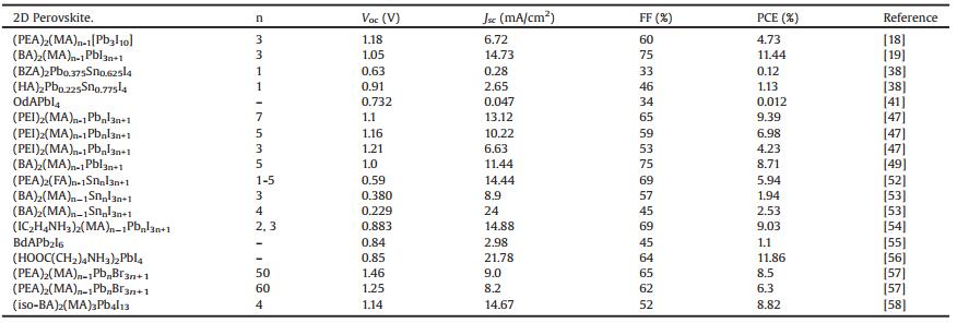
To improve the device stability of PSCs, alternatives to the 3D PVKs as the active absorber may be good choices. 2D PVK materials emerge recently as a promising candidate for photovoltaic applications. A maximum PCE of 12.5% with outstanding stability (2250 h) under light, humidity and heat stress has recently been attained from a 2D PSC [18, 19]. The PCE increase and several representative research articles recently published about 2D PSCs are shown in Fig. 1. It can be seen that since 2016 particularly in 2017, 2D PVKs and their solar cells attract more and more research interests. The high stability of 2D PVK can be attributed to its merit in structure, namely, the presence of strong hydrogen bonding of inorganic layers with organic layers and the high resistance of organic layers to humidity and light intensity [20]. In addition, layered 2D PVK materials can be easily deposited by simple, inexpensive techniques such as spin coating, vacuum vapors deposition and two steps dipping conversion methods [21, 22]. They also have potential applications in other fields of scintillation detectors for X-ray radiation, electroluminescence (EL) [23, 24] devices optical microcavities with strong exciton-photon coupling, and exciton or bi-exciton lasing [25, 26].

|
Download:
|
| Fig. 1. Increase of power conversion efficiencies and number of representative publications of the 2D PSCs. | |
In this review, we mainly highlight the structure and properties of recently reported 2D PVK materials and their related solar cell applications. More significantly, greater concentration will be given to compare the stability of 2D PSCs with 3D ones. Finally, we give an outlook on both achievements and challenges remaining in 2D PSCs.
2. Two-dimensional perovskite materials2D PVK materials have attracted the interest of researchers in the fields of optoelectronics, microelectronics, and particularly in photovoltaic devices [18, 27]. In fact, 2D PVK materials have extensive possibilities of chemical engineering with significant electronic and light absorption/emission properties at normal temperature [27, 28]. A 2D organic-inorganic PVK material offers hybrids properties of both organic and inorganic parts. The inorganic part shows a wide range of electronic properties, dielectric and magnetic transition, thermal stability, and mechanical hardness, while the organic part offers high polarizability, large fluorescence efficiency, structural diversity, and ease of processing [22]. Various properties of 2D PVK materials are illustrated in Fig. 2.

|
Download:
|
| Fig. 2. Properties of 2D layered organic-inorganic perovskite. | |
2.1. Structure of 2D PVK materials
The 2D PVK materials belong to the classical perovskite family, first introduced by two scientists S.N. Ruddlesden and P. Popper in 1957 [29], who originally synthesized and described the structure of 2D layered inorganic perovskite, having alternate slabs enclosed with cations. The layered structure was represented by general formula An-1A'BnX3n+1, where A, A', and B are cations, X is an anion, and n is the number of the layers of octahedra in the perovskite-like stack [30]. The 2D PVKs are analogues of Ruddlesden P. Popper (RP) phase structure, where A and A' are replaced by organic compounds and B is replaced by metal cation. The 2D PVK with layered structure may be supposed to be derived from the conventional 3D hybrid perovskite. If 3D hybrid perovskites are cut into one-layer-thick slices along the (100) direction and separated apart, the A and X-ions within the slice planes would be cut into halves. After the replacements of A and A' by appropriate organic molecules/ions (in general ammonium compounds), the single layer inorganic perovskite slabs are sandwiched by the organic molecules and the corresponding 2D perovskite is formed [22, 31]. The organic layer may be single layer or double layer, depending upon the type of ammonium cations. The typical examples of 2D organic-inorganic perovskites of (R-NH3)2MX4 and (NH3-R-NH3) MX4 with double and single organic layer having n = 1 are depicted in Fig. 3, where R-NH3+ and NH3+-R-NH3+ may be an aliphatic or aromatic ammonium cation(s), X represents the halogen, and M is a divalent metal ion such as Pb2+, Cu2+, Ni2+, Co2+, Fe2+, Mn2+, Cd2+, Pd2+, Ge2+, Sn2+, and Eu2+ [31].

|
Download:
|
| Fig. 3. Typical structures of the 2D layered hybrid organic–inorganic perovskite for n = 1 with double (a) and single (b) intercalated organic molecule layer. | |
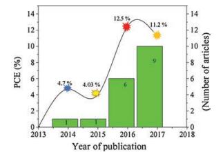
A variety of interactions are accountable for stabilizing the layered 2D PVK structures as compared to their 3D counterpart. The inorganic perovskite layer interacts either ionically or by hydrogen bond with the organic layer. The ammonium head(s) of the R-NH3 or NH3-R-NH3 cations can make hydrogen bond to any of the eight halogens (four bridging and four terminals) within the holes formed by the corners sharing with MX6 octahedra. Generally the NH3 group links either to one terminal halogen and two bridging halogens (bridging halogen configuration) or to one bridging halogen and two terminal halogens (terminal halogen configuration) to form hydrogen bonds (Fig. 4) [20]. The various members of RP phase types (n = 1-∞) are schematically shown in Fig. 5, which suggests that for infinite n value the 2D structure acquires classical 3D perovskite structure (AMX3) [22].

|
Download:
|
| Fig. 4. Hydrogen bonding arrangement in the oriented (100) 2D PVK, for the sake of simplicity methylammonium cations are presented here as the organic cations and hydrogens are removed from carbon atoms. Long alkyl chain ammoniums and aromatic cations have the same bonding scheme. | |

|
Download:
|
| Fig. 5. Representation of various members of 2D layered organic-inorganic perovskite for n = 1, 2, 3, and ∞. | |
2.2. Properties of 2D perovskite materials
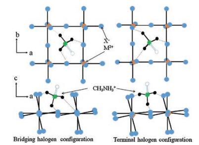
Interesting and unique physical properties were investigated in 2D PVK materials by studying their structures. The introduction of organic layer between the semiconducting perovskite layers greatly increases the flexibility for tuning the electrical properties of perovskite sheets [32]. The 2D PVK materials, especially those containing lead (Pb), tin (Sn), and germanium (Ge) halide perovskite sheets, behave like multilayer quantum well structures. The semiconducting inorganic perovskite forms alternate sheets with organic cations having relatively large HOMO-LUMO energy gap. Generally, the conduction band (CB) of the inorganic perovskite layer is lower than that of the organic layer, while the valence band (VB) of the inorganic perovskite is above that of the organic layer (Fig. 6a). Therefore, inorganic perovskite sheets act as a well both for holes and electrons. Moreover, the well and the barrier will be reversed, if a larger band gap metal halide perovskite sheets are treated with complex conjugated organic cations having low HOMO-LUMO gap (Fig. 6b). The band gap of organic and inorganic layers may be offset by choosing appropriate components of both organic and inorganic materials (Fig. 6c). The width of the barrier and well layer can easily be adjusted by changing the length of organic cation and the number of perovskite layers between each organic layer [33].

|
Download:
|
| Fig. 6. Illustration of several possible energy levels that arise within the structure of the 2D PVK materials. | |
The 2D PVK shows semiconductor-metal transition with increasing perovskite sheets (Fig. 7a) [34]. Recently the charge transport properties in 2D PVK materials were investigated by exploring the effect of MA to PEA ratio in ((PEA)2(MA)n-1PbnI3n+1) on charge carrier mobility, diffusion length, recombination dynamics, and orientation of the 2D PVKs (Fig. 7b) [35]. It was found that the charge carrier recombination rate first decreases with the increase of PEA concentration, which may be due to trap passivation, and then significantly increases owing to the domination of excitonic effect in perovskite thin layers [36].

|
Download:
|
| Fig. 7. (a) Resistivity (r) as a function of temperature for 2D PVK families (C4H9NH3)2(CH3NH3)n-1SnI3n+1 (black curves) and [NH2C(I) = NH2]2(CH3NH3)n-1SnI3n+1 (red curves). Copied with permission [34]. Copyright 1995, AAAS. (b) Schematic crystal structures of 3D PVK MAPbI3, 2D PVK (PEA)2PbI4, and intermediate mixed MA-PEA 2D perovskites. The %PEA labels indicate the mole percentage of PEA as a fraction of the total organic cation composition. Copied with permission [35]. Copyright 2016, American Chemical Society. | |
3. Solar cells based on 2D perovskite materials
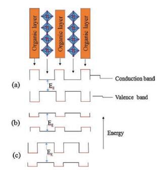
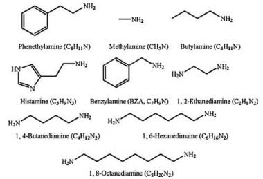
Due to desirable optical and electrical properties of 2D PVK materials, highly stable 2D PSCs have recently been fabricated from them by simple and cost-effective processing technology. The cations in these 2D PVKs are generally aliphatic and aromatic amines which could be classified into monoamines, diamines and multiamines. The names, structures and formulas of these amines are given in Fig. 8. Depending upon the type of amino compounds, 2D PSCs discussed here are also divided into three corresponding types. Moreover, some processing methods have been developed to change the crystal orientation of 2D PVK materials for enhanced device efficiency and lead-free 2D PSCs have also stepped into researchers' horizon, which will be discussed too in this section. Device performances of all 2D PSCs mentioned are listed in Table 1.

|
Download:
|
| Fig. 8. Structures, names and formulas of several types of aliphatic and aromatic amines recently reported in the 2D hybrid organic-inorganic perovskite solar cells. | |
|
|
Table 1 Summary of photovoltaic parameters of recently reported 2D perovskite solar cells. |
3.1. Solar cells based on monoamine-containing 2D perovskite materials
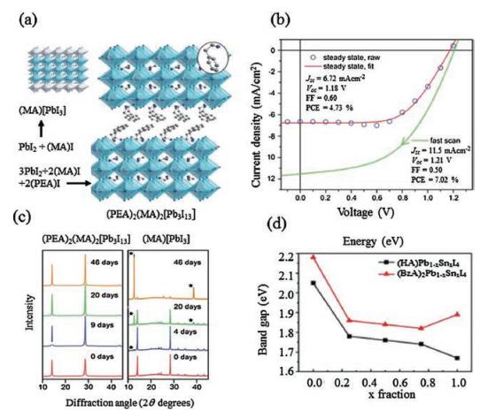
The first report about Ruddlesden P. Popper phase 2D PSC was published by Smith et al. in 2014, who employed (PEA)2(MA)2[Pb3I10] (PEA+ = phenethylamine cation) as the 2D PVK absorber. The crystal structure of (PEA)2(MA)2[Pb3I10] is shown in Fig. 9a, where the 3D perovskite layer is separated by PEA chain to form 2D layered structure. The fabricated 2D PSCs exhibit an overall PCE of 4.73% with a short-circuit current density (Jsc) of 6.72 mA/cm2, an open-circuit voltage (Voc) of 1.18 V, and a fill factor (FF) of 0.60 (Fig. 9b). Despite of a low PCE, the 2D PSC can be fabricated under humid condition (52% RH) and shows high moisture resistance under storage for 60 days (Fig. 9c) [18]. After one year (2105), Cao et al. developed a series of homologous 2D PVKs, (BA)2(MA)n-1PbI3n+1 (BA+ = n-butylammonium cation, n = 1- 4), synthesized by introducing bulkier primary organic ammonium cations, which confined the layered structure of perovskites. The device has an initial PCE of 4.02% with a Voc of 929 mV and a Jsc of 9.42 mA/cm2 with high stability in humid environment about two months. It was found that the lower efficiency of 2D PSCs compared to 3D ones may be due to the organic part that acted as the insulating layer counting against the flow of charges [37].

|
Download:
|
| Fig. 9. (a) Crystal structures of 2D PVK, (PEA)2(MA)2[Pb3I10] and 3D PVK, MAPbI3. (b) Current density-voltage (J-V) curve for the fabricated device. (c) XRD patterns of synthesized (PEA)2(MA)2[Pb3I10 after exposure to 52% humidity for certain days. Copied with permission [37]. Copyright 2014, Wiley-VCH Verlag GmbH & Co. K GaA. (d) Change in the band gap of 2D PVK with change in concentration of Sn. Copied with permission [38]. Copyright 2016, American Chemical Society. | |
Recently a new series of RP phase 2D PVK materials with mixed Pb/Sn was studied, consisting of aromatic dicationic histoamonium (HA) and monocationic benzylamonium (BZA). This study was carried out to explore the effect of charge difference and tin addition on the properties and device performance of 2D perovskite materials. Charge difference, greatly influences the orientation of the perovskite layers. HAPbI4 formed a perpendicular orientation to the substrate with a maximum device efficiency of 1.3%, as compared to BZAPbI4 which grew parallel to the substrate. Moreover, it has been found that the band gap of 2D PVK was greatly affected by varying the stoichiometric amount of Pb and Sn (Fig. 9d) [38].
3.2. Solar cells based on diamine-containing 2D perovskite materialsDue to structural similarity and a close relationship with monoammonium, diammonium series (NH2-(CH2)n-NH2) were also investigated in the near past for 2D PSCs. The two ammonium ions at both sides allow doubled hydrogen bonding with inorganic layers, which additionally increases the stability of the layered structure [39]. The hybrid layered 2D PVK ((EDA)(MA)2[Pb3I10]) (EDA = ethylenediamine) was recently synthesized by one-step method and their crystal structure, morphology, composition, and absorption spectra were characterized by grazing incidence X-ray diffraction (GIXRD), scanning electron microscope (SEM), and UV–vis spectroscopy, respectively. Fabricated solar cell based on (EDA)(MA)2[Pb3I10]) yielded a PCE of 11.58%, FF of 56%, a Jsc of 16.57 mA/cm2 and a Voc of 1.24 V). It was analyzed that 2PVK film based on EDA formed closely layered structures while 3D PVK film consisted of independent micro size grains. The external dense layer of (EDA)(MA)2[Pb3I10] protects the inner layer from degradation. Therefore, the stability of such a device showed higher resistant to humidity as compared to 3D PSCs [40]. Safdari et al. also reported a series of 2D PVKs materials based on diamines which are [NH3(CH2)4NH3]PbI4 (BdAPbI4), [NH3(CH2)6NH3]PbI4 (HdAPbI4), and [NH3(CH2)8NH3]PbI4 (OdAPbI4). These 2D PVKs were synthesized from the reaction between PbI2 and salt of 1, 4- diaminobutane, 1, 6-diaminohexane, and 1, 8-diaminooctane respectively. The devices based on these materials had higher stability than 3D PSCs, but afforded very low efficiencies, only about 1.08% [41].
3.3. Solar cells based on multiamine-containing 2D perovskite materialsThe key drawbacks of the 2D PVK materials are low charge mobility, great exciton binding energy, and significant increase in the band gap, due to less interaction between the organic layer and inorganic layer [42, 43]. It has been found that the introduction of multivalent organic cations can increase the interaction between two layers and consequently increasing the PCE as well as the stability of 2D PSCs [44]. The monoammonium cation like BA and PEA only interacts with one side of inorganic perovskite layers and hence there is a Van der Waals gap created between the layers, while multiammonium cation makes bonds with two adjacent inorganic perovskite layers spanning the entire distance between the layers [45]. The strong interaction between organic and inorganic layers greatly influences the band gap and crystal structure of the solid [43].
Recently a series of 2D perovskite compounds containing polyethyleneimine (PEI) cations ((PEI)2(MA)n-1PbnI3n+1 for n = 3, 4, 5, and 7) was investigated in 2D PSCs. The use of intercalated polyethyleneimine polymer cations induces tight stacking of adjacent perovskite layers, which further increases the stability and enhances the flow of charge. The charge transport within the layers and film quality of 2D PVK containing PEI were improved by enhancing the electronic integration in the adjacent layers as compared to those using small-molecule BA and PEA [46]. The PCE, Voc and Jsc of 2D PSC under ambient humidity are 8.77%, 1.0 V, and 11.7 mA/cm2, respectively. Although some 2D PSCs have been presented as discussed above, their efficiencies are still lower than 3D PSCs and thus needing further improvement [47].
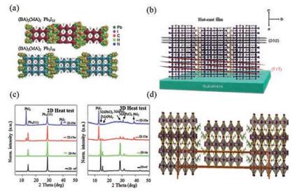
3.4. Methods for improved efficiency of 2D perovskite solar cellsThe direction of the inorganic perovskite layers and organic layers in 2D PSCs greatly influences the charge transport and thus the PCE [48]. When using the single step deposition method, 2D perovskite layers usually align parallel to the substrate, as a result of which the flow of photogenerated charges is limited within the inorganic layer, whereas the organic interlayer hinders the flow of charges as insulated layer, consequently resulting in low PCEs of 2D PSCs relative to 3D counterparts [18]. To overcome this issue, Koh et al. used a dipping deposition method based on a 2D PVK material (IC2H4NH3)2(CH3NH3)n-1PbnI3n+1 synthesized from iodoethylammonium iodide (IEAI), MAI and PbI2, under ambient condition (Fig. 10). With this method, the 2D PVK grew perpendicular to the substrate. The dimension of perovskite material was controlled using specific time duration. The increase in n value leads to a greater number of halide perovskite layers, showing lower band gap, stronger light absorption, and greater photocurrent. The 2D PSC base on this method has an overall PCE of 9.03% with a Voc of 883 mV, a Jsc of 14.83 mA/cm2, and a FF of 0.69. XRD analysis implied that the 2D PSCs exhibited long-term stability under 40% humidity at 25 ℃ without an encapsulation. Tsai et al. developed a new hot-casting method for the fabrication of 2D PVK [(BA)2(MA)n-1PbnI3n+1] (n = 3 and 2), and grew the perovskite perpendicular to the substrate by simply spin coating the precursor solution of 2D perovskite materials on a preheated substrate (FTO + PEDOT:PSS). The fabricated 2D PSC had better efficiency (12.5%) without any hysteresis and outstanding stability (2250 h) under light, humidity, and heat stress as compared to their 3D counterpart (Fig. 11) [19]. By using the hot-casting method, a high member of RP phase for n = 5 (BA)2(MA)4Pb5I16 was also successfully synthesized in pure form and its optical and electronic properties were measured (Fig. 11d). The fabricated solar cell also gave an excellent PCE (8.71%) with a Voc of 1.0 V [50].

|
Download:
|
| Fig. 10. (a) Fabrication process of 2DPVK materials(IC2H4NH3)2(CH3NH3)n-1PbnI3n+1) by dipping method. (b) Crystalline structure of 2D PVK, for n = 1 and 2. (c) Performance of the device made by dipping method for 4 min. (d) XRD patterns of the synthesized 2D PVK (IC2H4NH3)2(CH3NH3)n-1PbnI3n+1) at various times. Copied with permission [55]. Copyright 2016, Wiley-VCH Verlag GmbH & Co. KGaA. | |

|
Download:
|
| Fig. 11. (a) Structure of Ruddlesen-Popper (RP) type perovskite (BA)2(MA)2Pb3I10 and (BA)2(MA)3Pb4I13 prepared by hot casting method. (b) Schematic demonstration of 2D perovskite crystal orientation along the (101), (202), and (111) planes. (c) XRD patterns of 2D and 3D PVKs after storing for specific times. Copied with permission [19]. Copyright 2016, Nature Publishing Group. (d) Crystal structure of (BA)2(MA)4Pb5I16 for n = 5. Copied with permission [49]. Copyright 2017, Elsevier. | |
3.5. Lead-free 2D perovskite solar cell
Although 2D PVK materials and their solar cells have made considerable progresses, toxicity of Pb in the 2D PVKs has bottlenecked the further development of 2D PSCs, similar to the situation of 3D PSCs. Basically, Pb is toxic to the environments and hard to excrete from the body [51]. The standard accepted level of Pb set by U.S. EPA is 15 μg/L and 0.15 μg/L for water and air, respectively. The decomposition of lead-containing perovskite releases Pb2+, having larger solubility (Ksp: 1 ×10⁻⁸) than conventional toxic Cd in CdTe (Ksp: 1 ×10-22), which has been recycled due to its toxicity [52]. Therefore, despite of high performance of lead-based 2D PSCs, it is also essential to explore environmental friendly metal ions for the further development of 2D PSCs. Liao et al. demonstrated lead-free tin based 2D PVK materials (PEA)2(FA)n-1SnnI3n+1) for solar cell application. The fabricated 2D PSCs have a maximum PCE of 5.95%, a Voc of 0.59 V, a Jsc of 14.44 mA/cm2, and a FF of 69%. The device efficiency and stability based on this lead-free 2D PVK are higher than those from the 3D counterpart, e.g. FASnI3 [53]. Cao et al. very recently reported Sn-based RP phase 2D PVK (CH3(CH2)3NH3)2-(CH3NH3)n-1SnnI3n+1, which exhibited highly resistant to moisture in 2D PSCs relative to 3D MASnI3, with a PCE of only 2.5% [54].
4. Conclusions and outlooksWe have reviewed recent progress in 2D PVK materials as the active absorber for solar cell application. Although the PCEs of 2D PSCs are still modest as compared to those of 3D ones, the former has manifested much superior stability upon exposure to heat, humidity, and light intensity. In particular, a highly stable 2D/3D PSC (up to one year stable) was reported with a maximum PCE of 11.2% very recently [56], which makes researchers working on PVK materials and their solar cells more confident in the improvement of both the efficiency and the stability. Major breakthroughs not only in these two aspects but also in the avoidable usage of lead can be anticipated in the near future, which requires remarkable efforts on several research topics as followings. 1) Deep understanding on the structure, dimensionality, and charge transport property of 2D PVK materials, which correlates with the device performance of 2D PSCs; 2) Employment of various amine compounds for further exploration of new 2D PVK materials for photovoltaic applications; 3) Partial or full substitution of iodine in the 2D PVKs with bromine or other halides, such as a 2D PVK of (PEA)2(MA)n–1PbnBr3n+1 reported recently [57]; 4) Replacement of MA by FA for raising photovoltaic performance of 2D PSCs [59]; 5) Development of new 2D PVK materials with Sn or other metal ions for lead-free 2D PSCs; 6) Invention of novel processing approaches to adjust the aligned direction of 2D PVK crystal to enhance the device efficiency. Beyond these, upscaling, cost control, and so on should be also taken into account. Use of 2D PVKs for solar cells is still in its infancy but studies on such topics are believed to enable a bright future for the 2D PSCs. This review summarizes latest research progress and is hoped to inspire future developments in 2D perovskite materials for photovoltaics.
AcknowledgmentsThis work was financially supported by the "Thousand Talents Program for Young Scholars" of China, the National Natural Science Foundation of China (No. 21644008), and the Collaborative Innovation Center of Chemistry for Energy Materials (iChEM).
| [1] |
T. Miyasaka, A. Kojima, K. Teshima, Y. Shirai, J. Am. Chem. Soc. 131 (2009) 6050-6051. DOI:10.1021/ja809598r |
| [2] |
J.F. Liao, H.S. Rao, B.X. Chen, D.B. Kuang, C.Y. Su, J. Mater. Chem. A 5 (2016) 2066-2072. |
| [3] |
F. Ullah, H. Chen, C. Li, Chin. Chem. Lett. 28 (2017) 503-511. DOI:10.1016/j.cclet.2016.11.009 |
| [4] |
W. Jiang, J. Ying, W. Zhou, et al., Chem. Phys. Lett. 658 (2016) 71-75. DOI:10.1016/j.cplett.2016.05.054 |
| [5] |
M. Yuan, L.N. Quan, R. Comin, et al., Nat. Nanotechnol. 11 (2016) 872-877. DOI:10.1038/nnano.2016.110 |
| [6] |
K.T. Cho, S. Paek, G. Grancini, et al., Energy Environ. Sci. 10 (2017) 621-627. DOI:10.1039/C6EE03182J |
| [7] |
M. Pandey, K.W. Jacobsen, K.S. Thygesen, J. Phys. Chem. Lett. 7 (2016) 4346-4352. DOI:10.1021/acs.jpclett.6b01998 |
| [8] |
M. Saliba, T. Matsui, K. Domanski, et al., Science 354 (2016) 206-209. DOI:10.1126/science.aah5557 |
| [9] |
H. Kim, J. Seo, N. Park, ChemSusChem 9 (2016) 2528-2540. DOI:10.1002/cssc.201600915 |
| [10] |
J.H. Noh, S.H. Im, J.H. Heo, T.N. Mandal, Il Seok S., Nano Lett. 13 (2013) 1764-1769. DOI:10.1021/nl400349b |
| [11] |
S. Yang, W. Fu, Z. Zhang, H. Chen, C.Z. Li, J. Mater. Chem. A 5 (2017) 11462-11482. DOI:10.1039/C7TA00366H |
| [12] |
Y. Zhang, M. Liu, G.E. Eperon, et al., Mater. Horiz. 2 (2015) 315-322. DOI:10.1039/C4MH00238E |
| [13] |
X. Li, M.I. Dar, C. Yi, et al., Nat. Chem. 7 (2015) 703-711. DOI:10.1038/nchem.2324 |
| [14] |
J. You, L. Meng, T.B. Song, et al., Nat. Nanotechnol. 11 (2015) 75-81. DOI:10.1038/nnano.2015.230 |
| [15] |
K. Aitola, K. Domanski, J.P. Correa-Baena, et al., Adv. Mater. 29 (2017) 1606398. DOI:10.1002/adma.v29.17 |
| [16] |
S.N. Habisreutinger, T. Leijtens, G.E. Eperon, et al., Nano Lett. 14 (2014) 5561-5568. DOI:10.1021/nl501982b |
| [17] |
F. Bella, G. Griffini, J.P. Correa-Baena, et al., Science 354 (2016) 203-206. DOI:10.1126/science.aah4046 |
| [18] |
I.C. Smith, E.T. Hoke, D. Solis-Ibarra, M.D. McGehee, H.I. Karunadasa, Angew. Chem. Int. Ed. 126 (2014) 11414-11417. DOI:10.1002/ange.201406466 |
| [19] |
H. Tsai, W. Nie, J.C. Blancon, et al., Nature 536 (2016) 312-316. DOI:10.1038/nature18306 |
| [20] |
D. B. Mizi, Synthesis, Structure, and Properties of Organic-inorganic Perovskites and Related Materials, John Wiley and Sons, Inc, New York, 2007, pp. 1-121.
|
| [21] |
J. Chen, L. Gan, F. Zhuge, et al., Angew. Chem. Int. Ed. 129 (2017) 2430-2434. DOI:10.1002/ange.201611794 |
| [22] |
K. Chondroudis, C.R. Kagan, IBM J. Res. Dev. 45 (2001) 29-45. DOI:10.1147/rd.451.0029 |
| [23] |
S. Kishimoto, K. Shibuya, F. Nishikido, et al., Appl. Phys. Lett. 93 (2008) 261901. DOI:10.1063/1.3059562 |
| [24] |
M. Era, S. Morimoto, T. Tsutsui, S. Saito, Appl. Phys. Lett. 65 (1994) 676-678. DOI:10.1063/1.112265 |
| [25] |
K. Pradeesh, J.J. Baumberg, G.V. Prakash, Opt. Express 17 (2009) 22171-22178. DOI:10.1364/OE.17.022171 |
| [26] |
G. Lanty, J.S. Lauret, E. Deleporte, S. Bouchoule, X. Lafosse, Appl. Phys. Lett. 93 (2008) 81101. DOI:10.1063/1.2971206 |
| [27] |
L. Pedesseau, D. Sapori, B. Traore, et al., ACS Nano. 10 (2016) 9776-9786. DOI:10.1021/acsnano.6b05944 |
| [28] |
M. Pandey, K.W. Jacobsen, K.S. Thygesen, J. Phys. Chem. Lett. 7 (2016) 4346-4352. DOI:10.1021/acs.jpclett.6b01998 |
| [29] |
B.V. Beznosikov, K.S. Aleksandrov, Crystallogr. Reports 45 (2000) 792-798. DOI:10.1134/1.1312923 |
| [30] |
S.N. Ruddlesden, P. Popper, Acta Crystallogr. 11 (1958) 54-55. DOI:10.1107/S0365110X58000128 |
| [31] |
Z. Cheng, J. Lin, CrystEngComm 12 (2010) 2646-2662. DOI:10.1039/c001929a |
| [32] |
D.B. Mitzi, C.A. Feild, W.T.A. Harrison, A.M. Guloy, Nature 369 (1994) 467-469. DOI:10.1038/369467a0 |
| [33] |
X. Hong, T. Ishihara, A.V. Nurmikko, Phys. Rev. B 45 (1992) 6961-6964. DOI:10.1103/PhysRevB.45.6961 |
| [34] |
D.B. Mitzi, S. Wang, C.A. Feild, C.A. Chess, A.M. Guloy, Science 267 (1995) 1473-1476. DOI:10.1126/science.267.5203.1473 |
| [35] |
R.L. Milot, R.J. Sutton, G.E. Eperon, et al., Nano Lett. 16 (2016) 7001-7007. DOI:10.1021/acs.nanolett.6b03114 |
| [36] |
X. Hong, T. Ishihara, A.V. Nurmikko, Phys. Rev. B. 45 (1992) 6961-6964. DOI:10.1103/PhysRevB.45.6961 |
| [37] |
D.H. Cao, C.C. Stoumpos, O.K. Farha, J.T. Hupp, M.G. Kanatzidis, J. Am. Chem. Soc. 137 (2015) 7843-7850. DOI:10.1021/jacs.5b03796 |
| [38] |
L. Mao, H. Tsai, W. Nie, et al., Chem. Mater. 28 (2016) 7781-7792. DOI:10.1021/acs.chemmater.6b03054 |
| [39] |
S.K. Abdel-Aal, A.S. Abdel-Rahman, J. Cryst. Growth 457 (2017) 282-288. DOI:10.1016/j.jcrysgro.2016.08.006 |
| [40] |
W. Jiang, J. Ying, W. Zhou, et al., Chem. Phys. Lett. 658 (2016) 71-75. DOI:10.1016/j.cplett.2016.05.054 |
| [41] |
M. Safdari, P.H. Svensson, M.T. Hoang, et al., J. Mater. Chem. A 4 (2016) 15638-15646. DOI:10.1039/C6TA05055G |
| [42] |
E.R. Dohner, A. Jaffe, L.R. Bradshaw, H.I. Karunadasa, J. Am. Chem. Soc. 136 (2014) 13154-13157. DOI:10.1021/ja507086b |
| [43] |
S. Sourisseau, N. Louvain, W. Bi, et al., Chem. Mater. 19 (2007) 600-607. DOI:10.1021/cm062380e |
| [44] |
H. Hu, T. Salim, B. Chen, Y.M. Lam, Sci. Rep. 6 (2016) 33546. DOI:10.1038/srep33546 |
| [45] |
E.R. Dohner, A. Jaffe, L.R. Bradshaw, H.I. Karunadasa, J. Am. Chem. Soc. 136 (2014) 13154-13157. DOI:10.1021/ja507086b |
| [46] |
N. Mercier, A. Riou, Chem. Commun. 33 (2004) 844-845. |
| [47] |
K. Yao, X. Wang, Y.X. Xu, F. Li, L. Zhou, Chem. Mater. 28 (2016) 3131-3138. DOI:10.1021/acs.chemmater.6b00711 |
| [48] |
D.B. Mitzi, J. Mater. Chem. 14 (2004) 2355-2365. DOI:10.1039/b403482a |
| [49] |
T.M. Koh, V. Shanmugam, J. Schlipf, et al., Adv. Mater 28 (2016) 3653-3661. DOI:10.1002/adma.201506141 |
| [50] |
C.C. Stoumpos, C.M.M. Soe, H. Tsai, et al., Chem. 2 (2017) 427-440. DOI:10.1016/j.chempr.2017.02.004 |
| [51] |
Z. Shi, J. Guo, Y. Chen, et al., Adv. Mater. 29 (2017) 1605005. DOI:10.1002/adma.201605005 |
| [52] |
P. Patnaik, Handbook of Inorganic Chemicals[M]. New Yor: McGraw-Hill, 2003.
|
| [53] |
Y. Liao, H. Liu, W. Zhou, et al., J. Am. Chem. Soc. 139 (2017) 6693-6699. DOI:10.1021/jacs.7b01815 |
| [54] |
D.H. Cao, C.C. Stoumpos, T. Yokoyama, et al., ACS Energy Lett. (2017), 982-990. |
| [55] |
M. Safdari, D. Phuyal, B. Philippe, et al., J. Mater. Chem. A 5 (2017) 11730-11738. DOI:10.1039/C6TA10123B |
| [56] |
G. Grancini, C. Roldán-Carmona, I. Zimmermann, et al., Nat. Commun. 8 (2017) 15684. DOI:10.1038/ncomms15684 |
| [57] |
B. Cohen, M. Wierzbowska, L. Etgar, Adv. Funct. Mater. 27 (2017) 1604733. DOI:10.1002/adfm.v27.5 |
| [58] |
Y. Chen, Y. Sun, J. Peng, et al., Adv. Energy Mater. 7 (2017) 1700162. DOI:10.1002/aenm.201700162 |
| [59] |
R. Hamagu chi, M. Yoshizawa-Fujita, T. Miyasaka, et al., Chem. Commun. 53 (2017) 4366-4369. DOI:10.1039/C7CC00921F |